JP5381821B2 - 保護テープ剥離方法および保護テープ剥離装置 - Google Patents
保護テープ剥離方法および保護テープ剥離装置 Download PDFInfo
- Publication number
- JP5381821B2 JP5381821B2 JP2010053447A JP2010053447A JP5381821B2 JP 5381821 B2 JP5381821 B2 JP 5381821B2 JP 2010053447 A JP2010053447 A JP 2010053447A JP 2010053447 A JP2010053447 A JP 2010053447A JP 5381821 B2 JP5381821 B2 JP 5381821B2
- Authority
- JP
- Japan
- Prior art keywords
- protective tape
- wafer
- peeling
- tape
- lift pin
- Prior art date
- Legal status (The legal status is an assumption and is not a legal conclusion. Google has not performed a legal analysis and makes no representation as to the accuracy of the status listed.)
- Expired - Fee Related
Links
Images




Classifications
-
- B—PERFORMING OPERATIONS; TRANSPORTING
- B65—CONVEYING; PACKING; STORING; HANDLING THIN OR FILAMENTARY MATERIAL
- B65H—HANDLING THIN OR FILAMENTARY MATERIAL, e.g. SHEETS, WEBS, CABLES
- B65H3/00—Separating articles from piles
- B65H3/32—Separating articles from piles by elements, e.g. fingers, plates, rollers, inserted or traversed between articles to be separated and remainder of the pile
-
- B—PERFORMING OPERATIONS; TRANSPORTING
- B32—LAYERED PRODUCTS
- B32B—LAYERED PRODUCTS, i.e. PRODUCTS BUILT-UP OF STRATA OF FLAT OR NON-FLAT, e.g. CELLULAR OR HONEYCOMB, FORM
- B32B43/00—Operations specially adapted for layered products and not otherwise provided for, e.g. repairing; Apparatus therefor
- B32B43/006—Delaminating
-
- B—PERFORMING OPERATIONS; TRANSPORTING
- B32—LAYERED PRODUCTS
- B32B—LAYERED PRODUCTS, i.e. PRODUCTS BUILT-UP OF STRATA OF FLAT OR NON-FLAT, e.g. CELLULAR OR HONEYCOMB, FORM
- B32B38/00—Ancillary operations in connection with laminating processes
- B32B38/10—Removing layers, or parts of layers, mechanically or chemically
-
- H—ELECTRICITY
- H10—SEMICONDUCTOR DEVICES; ELECTRIC SOLID-STATE DEVICES NOT OTHERWISE PROVIDED FOR
- H10P—GENERIC PROCESSES OR APPARATUS FOR THE MANUFACTURE OR TREATMENT OF DEVICES COVERED BY CLASS H10
- H10P72/00—Handling or holding of wafers, substrates or devices during manufacture or treatment thereof
- H10P72/04—Apparatus for manufacture or treatment
- H10P72/0442—Apparatus for placing on an insulating substrate, e.g. tape
-
- B—PERFORMING OPERATIONS; TRANSPORTING
- B32—LAYERED PRODUCTS
- B32B—LAYERED PRODUCTS, i.e. PRODUCTS BUILT-UP OF STRATA OF FLAT OR NON-FLAT, e.g. CELLULAR OR HONEYCOMB, FORM
- B32B2457/00—Electrical equipment
- B32B2457/14—Semiconductor wafers
-
- H—ELECTRICITY
- H10—SEMICONDUCTOR DEVICES; ELECTRIC SOLID-STATE DEVICES NOT OTHERWISE PROVIDED FOR
- H10P—GENERIC PROCESSES OR APPARATUS FOR THE MANUFACTURE OR TREATMENT OF DEVICES COVERED BY CLASS H10
- H10P72/00—Handling or holding of wafers, substrates or devices during manufacture or treatment thereof
- H10P72/70—Handling or holding of wafers, substrates or devices during manufacture or treatment thereof for supporting or gripping
- H10P72/74—Handling or holding of wafers, substrates or devices during manufacture or treatment thereof for supporting or gripping using temporarily an auxiliary support
- H10P72/7402—Wafer tapes, e.g. grinding or dicing support tapes
-
- H—ELECTRICITY
- H10—SEMICONDUCTOR DEVICES; ELECTRIC SOLID-STATE DEVICES NOT OTHERWISE PROVIDED FOR
- H10P—GENERIC PROCESSES OR APPARATUS FOR THE MANUFACTURE OR TREATMENT OF DEVICES COVERED BY CLASS H10
- H10P72/00—Handling or holding of wafers, substrates or devices during manufacture or treatment thereof
- H10P72/70—Handling or holding of wafers, substrates or devices during manufacture or treatment thereof for supporting or gripping
- H10P72/74—Handling or holding of wafers, substrates or devices during manufacture or treatment thereof for supporting or gripping using temporarily an auxiliary support
- H10P72/7416—Handling or holding of wafers, substrates or devices during manufacture or treatment thereof for supporting or gripping using temporarily an auxiliary support used during dicing or grinding
-
- H—ELECTRICITY
- H10—SEMICONDUCTOR DEVICES; ELECTRIC SOLID-STATE DEVICES NOT OTHERWISE PROVIDED FOR
- H10P—GENERIC PROCESSES OR APPARATUS FOR THE MANUFACTURE OR TREATMENT OF DEVICES COVERED BY CLASS H10
- H10P72/00—Handling or holding of wafers, substrates or devices during manufacture or treatment thereof
- H10P72/70—Handling or holding of wafers, substrates or devices during manufacture or treatment thereof for supporting or gripping
- H10P72/74—Handling or holding of wafers, substrates or devices during manufacture or treatment thereof for supporting or gripping using temporarily an auxiliary support
- H10P72/744—Details of chemical or physical process used for separating the auxiliary support from a device or a wafer
- H10P72/7442—Separation by peeling
-
- Y—GENERAL TAGGING OF NEW TECHNOLOGICAL DEVELOPMENTS; GENERAL TAGGING OF CROSS-SECTIONAL TECHNOLOGIES SPANNING OVER SEVERAL SECTIONS OF THE IPC; TECHNICAL SUBJECTS COVERED BY FORMER USPC CROSS-REFERENCE ART COLLECTIONS [XRACs] AND DIGESTS
- Y10—TECHNICAL SUBJECTS COVERED BY FORMER USPC
- Y10S—TECHNICAL SUBJECTS COVERED BY FORMER USPC CROSS-REFERENCE ART COLLECTIONS [XRACs] AND DIGESTS
- Y10S156/00—Adhesive bonding and miscellaneous chemical manufacture
- Y10S156/918—Delaminating processes adapted for specified product, e.g. delaminating medical specimen slide
- Y10S156/93—Semiconductive product delaminating, e.g. delaminating emiconductive wafer from underlayer
- Y10S156/931—Peeling away backing
- Y10S156/932—Peeling away backing with poking during delaminating, e.g. jabbing release sheet backing to remove wafer
-
- Y—GENERAL TAGGING OF NEW TECHNOLOGICAL DEVELOPMENTS; GENERAL TAGGING OF CROSS-SECTIONAL TECHNOLOGIES SPANNING OVER SEVERAL SECTIONS OF THE IPC; TECHNICAL SUBJECTS COVERED BY FORMER USPC CROSS-REFERENCE ART COLLECTIONS [XRACs] AND DIGESTS
- Y10—TECHNICAL SUBJECTS COVERED BY FORMER USPC
- Y10S—TECHNICAL SUBJECTS COVERED BY FORMER USPC CROSS-REFERENCE ART COLLECTIONS [XRACs] AND DIGESTS
- Y10S156/00—Adhesive bonding and miscellaneous chemical manufacture
- Y10S156/934—Apparatus having delaminating means adapted for delaminating a specified article
- Y10S156/941—Means for delaminating semiconductive product
- Y10S156/943—Means for delaminating semiconductive product with poking delaminating means, e.g. jabbing means
-
- Y—GENERAL TAGGING OF NEW TECHNOLOGICAL DEVELOPMENTS; GENERAL TAGGING OF CROSS-SECTIONAL TECHNOLOGIES SPANNING OVER SEVERAL SECTIONS OF THE IPC; TECHNICAL SUBJECTS COVERED BY FORMER USPC CROSS-REFERENCE ART COLLECTIONS [XRACs] AND DIGESTS
- Y10—TECHNICAL SUBJECTS COVERED BY FORMER USPC
- Y10T—TECHNICAL SUBJECTS COVERED BY FORMER US CLASSIFICATION
- Y10T156/00—Adhesive bonding and miscellaneous chemical manufacture
- Y10T156/11—Methods of delaminating, per se; i.e., separating at bonding face
- Y10T156/1168—Gripping and pulling work apart during delaminating
- Y10T156/1179—Gripping and pulling work apart during delaminating with poking during delaminating [e.g., jabbing, etc.]
-
- Y—GENERAL TAGGING OF NEW TECHNOLOGICAL DEVELOPMENTS; GENERAL TAGGING OF CROSS-SECTIONAL TECHNOLOGIES SPANNING OVER SEVERAL SECTIONS OF THE IPC; TECHNICAL SUBJECTS COVERED BY FORMER USPC CROSS-REFERENCE ART COLLECTIONS [XRACs] AND DIGESTS
- Y10—TECHNICAL SUBJECTS COVERED BY FORMER USPC
- Y10T—TECHNICAL SUBJECTS COVERED BY FORMER US CLASSIFICATION
- Y10T156/00—Adhesive bonding and miscellaneous chemical manufacture
- Y10T156/19—Delaminating means
- Y10T156/1978—Delaminating bending means
- Y10T156/1983—Poking delaminating means
Landscapes
- Engineering & Computer Science (AREA)
- Mechanical Engineering (AREA)
- Container, Conveyance, Adherence, Positioning, Of Wafer (AREA)
Description
本発明の実施の形態1にかかる保護テープ剥離方法および保護テープ剥離装置について図1ないし図13を参照して説明する。なお、同一又は対応する構成要素には同一の符号を付して説明の繰り返しを省略する場合がある。他の実施の形態でも同様である。
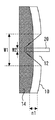
本発明の実施の形態2にかかる保護テープ剥離方法および保護テープ剥離装置について図14ないし図16を参照して説明する。実施の形態1と同様の構成要素には同じ符号を用いる。以後、実施の形態1との相違点を中心に説明する。
Claims (2)
- ウエハのノッチを覆う第1の部分と前記ウエハの外縁より外側へはみ出す第2の部分とを有する保護テープが貼り付けられた前記ウエハを、ステージに載せる工程と、
剥離用粘着テープを前記保護テープに貼り付ける工程と、
前記ステージからリフトピンを突出させて、前記リフトピンの上面により前記第1の部分および前記第2の部分を持ち上げる工程と、
前記リフトピンにより前記保護テープを持ち上げた状態で前記剥離用粘着テープを引っ張り、前記保護テープを前記ウエハから剥離する工程とを備え、
前記リフトピンの上面形状は、幅狭部と幅広部を有し、前記幅狭部が前記第1の部分を持ち上げ、前記幅広部が前記第2の部分を持ち上げることを特徴とする保護テープ剥離方法。 - ウエハのノッチを覆う第1の部分と前記ウエハの外縁より外側へはみ出す第2の部分とを有する保護テープが貼り付けられた前記ウエハを載せるステージと、
前記保護テープに剥離用粘着テープを貼り付ける手段と、
前記剥離用粘着テープを剥離する手段と、
前記ステージから突出することが可能なように前記ステージに取り付けられたリフトピンとを備え、
前記リフトピンの上面形状は、幅狭部と幅広部を有し、前記幅狭部が前記第1の部分を持ち上げ、前記幅広部が前記第2の部分を持ち上げることができる形状であることを特徴とする保護テープ剥離装置。
Priority Applications (6)
| Application Number | Priority Date | Filing Date | Title |
|---|---|---|---|
| JP2010053447A JP5381821B2 (ja) | 2010-03-10 | 2010-03-10 | 保護テープ剥離方法および保護テープ剥離装置 |
| TW099146152A TWI431680B (zh) | 2010-03-10 | 2010-12-27 | 保護膠帶剝離方法及保護膠帶剝離裝置 |
| US12/979,844 US20110220296A1 (en) | 2010-03-10 | 2010-12-28 | Method and apparatus for peeling protective tape |
| DE102011004155.9A DE102011004155B4 (de) | 2010-03-10 | 2011-02-15 | Verfahren und Gerät zum Abziehen eines Schutzbandes |
| CN201110059688.7A CN102205687B (zh) | 2010-03-10 | 2011-03-09 | 保护带剥离方法以及保护带剥离装置 |
| US13/715,218 US8778133B2 (en) | 2010-03-10 | 2012-12-14 | Method and apparatus for peeling protective tape |
Applications Claiming Priority (1)
| Application Number | Priority Date | Filing Date | Title |
|---|---|---|---|
| JP2010053447A JP5381821B2 (ja) | 2010-03-10 | 2010-03-10 | 保護テープ剥離方法および保護テープ剥離装置 |
Publications (2)
| Publication Number | Publication Date |
|---|---|
| JP2011187827A JP2011187827A (ja) | 2011-09-22 |
| JP5381821B2 true JP5381821B2 (ja) | 2014-01-08 |
Family
ID=44508075
Family Applications (1)
| Application Number | Title | Priority Date | Filing Date |
|---|---|---|---|
| JP2010053447A Expired - Fee Related JP5381821B2 (ja) | 2010-03-10 | 2010-03-10 | 保護テープ剥離方法および保護テープ剥離装置 |
Country Status (5)
| Country | Link |
|---|---|
| US (2) | US20110220296A1 (ja) |
| JP (1) | JP5381821B2 (ja) |
| CN (1) | CN102205687B (ja) |
| DE (1) | DE102011004155B4 (ja) |
| TW (1) | TWI431680B (ja) |
Families Citing this family (6)
| Publication number | Priority date | Publication date | Assignee | Title |
|---|---|---|---|---|
| CN104779192B (zh) * | 2014-01-10 | 2017-10-27 | 上海华虹宏力半导体制造有限公司 | 用于晶片背面减薄研磨制程的晶片缺口处保护胶切割方法 |
| JP6301685B2 (ja) * | 2014-03-04 | 2018-03-28 | 株式会社ディスコ | 保護テープ剥離装置及び保護テープ剥離方法 |
| TWI685905B (zh) * | 2017-07-12 | 2020-02-21 | 日商新川股份有限公司 | 接合裝置和接合方法 |
| JP7320932B2 (ja) * | 2017-11-10 | 2023-08-04 | 芝浦メカトロニクス株式会社 | 成膜装置及び部品剥離装置 |
| KR102640172B1 (ko) | 2019-07-03 | 2024-02-23 | 삼성전자주식회사 | 기판 처리 장치 및 이의 구동 방법 |
| CN113013080A (zh) * | 2021-02-24 | 2021-06-22 | 中芯集成电路制造(绍兴)有限公司 | 揭膜方法 |
Family Cites Families (17)
| Publication number | Priority date | Publication date | Assignee | Title |
|---|---|---|---|---|
| KR19990028523A (ko) * | 1995-08-31 | 1999-04-15 | 야마모토 히데키 | 반도체웨이퍼의 보호점착테이프의 박리방법 및 그 장치 |
| JPH09115863A (ja) * | 1995-10-23 | 1997-05-02 | Oki Electric Ind Co Ltd | 表面保護テープ貼り付け方法およびその装置 |
| US6202292B1 (en) * | 1998-08-26 | 2001-03-20 | Micron Technology, Inc. | Apparatus for removing carrier film from a semiconductor die |
| CN1260779C (zh) * | 2001-06-11 | 2006-06-21 | 日东电工株式会社 | 从半导体晶片上清除无用物质的方法和装置 |
| JP2003209082A (ja) | 2002-01-15 | 2003-07-25 | Nitto Denko Corp | 保護テープの貼付方法およびその装置並びに保護テープの剥離方法 |
| JP4316187B2 (ja) * | 2002-05-20 | 2009-08-19 | リンテック株式会社 | 脆質材料の剥離方法及び剥離装置 |
| JP2004128147A (ja) * | 2002-10-01 | 2004-04-22 | Nitto Denko Corp | 半導体ウエハからの保護テープ除去方法およびその装置 |
| KR100532287B1 (ko) * | 2003-09-17 | 2005-11-29 | 삼성전자주식회사 | 휴대용 카메라 모듈의 미세 이물질 제거 장치 및 방법 |
| JP4538242B2 (ja) * | 2004-01-23 | 2010-09-08 | 株式会社東芝 | 剥離装置及び剥離方法 |
| JP4297829B2 (ja) * | 2004-04-23 | 2009-07-15 | リンテック株式会社 | 吸着装置 |
| US7240422B2 (en) * | 2004-05-11 | 2007-07-10 | Asm Assembly Automation Ltd. | Apparatus for semiconductor chip detachment |
| KR100983910B1 (ko) | 2005-11-04 | 2010-09-28 | 도쿄 세이미츄 코퍼레이션 리미티드 | 필름 박리 방법 및 필름 박리 장치 |
| JP4698517B2 (ja) * | 2006-04-18 | 2011-06-08 | 日東電工株式会社 | 保護テープ剥離方法およびこれを用いた装置 |
| JP4353975B2 (ja) * | 2006-11-29 | 2009-10-28 | 日東電工株式会社 | 粘着シートの貼付・剥離方法及び粘着シートの貼付装置並びに粘着シートの剥離装置 |
| JP2009099865A (ja) * | 2007-10-18 | 2009-05-07 | Toyota Motor Corp | 保護テープの除去装置と除去方法 |
| JP5061324B2 (ja) * | 2007-11-13 | 2012-10-31 | 株式会社タカトリ | ウエハの保護テープの剥離方法及び装置 |
| JP5222756B2 (ja) * | 2009-02-24 | 2013-06-26 | リンテック株式会社 | 剥離装置及び剥離方法 |
-
2010
- 2010-03-10 JP JP2010053447A patent/JP5381821B2/ja not_active Expired - Fee Related
- 2010-12-27 TW TW099146152A patent/TWI431680B/zh not_active IP Right Cessation
- 2010-12-28 US US12/979,844 patent/US20110220296A1/en not_active Abandoned
-
2011
- 2011-02-15 DE DE102011004155.9A patent/DE102011004155B4/de not_active Expired - Fee Related
- 2011-03-09 CN CN201110059688.7A patent/CN102205687B/zh not_active Expired - Fee Related
-
2012
- 2012-12-14 US US13/715,218 patent/US8778133B2/en not_active Expired - Fee Related
Also Published As
| Publication number | Publication date |
|---|---|
| TWI431680B (zh) | 2014-03-21 |
| DE102011004155A1 (de) | 2011-09-15 |
| CN102205687A (zh) | 2011-10-05 |
| US20130098542A1 (en) | 2013-04-25 |
| US20110220296A1 (en) | 2011-09-15 |
| DE102011004155B4 (de) | 2014-02-13 |
| US8778133B2 (en) | 2014-07-15 |
| JP2011187827A (ja) | 2011-09-22 |
| TW201135824A (en) | 2011-10-16 |
| CN102205687B (zh) | 2014-08-06 |
Similar Documents
| Publication | Publication Date | Title |
|---|---|---|
| JP5381821B2 (ja) | 保護テープ剥離方法および保護テープ剥離装置 | |
| KR100766512B1 (ko) | 반도체 칩의 박리 방법 및 장치 | |
| JP3865184B2 (ja) | 半導体装置の製造方法 | |
| JP2008042016A (ja) | 半導体ウエハの保持方法および半導体ウエハ保持構造体 | |
| CN101312118A (zh) | 半导体晶圆的保护方法 | |
| US20160071808A1 (en) | Integrated semiconductor device and method for fabricating the same | |
| JP2009044008A (ja) | ウエハの保護テープ剥離方法及び装置 | |
| JP5399648B2 (ja) | 接着シート及びこれを用いた半導体ウエハの処理方法 | |
| US20150262854A1 (en) | Wafer etching system and wafer etching process using the same | |
| JP2010283097A (ja) | 両面接着シート | |
| CN108231567B (zh) | 一种晶背减薄方法及所使用的圆形治具 | |
| JP2013168616A (ja) | 保護テープ剥離方法 | |
| JP5214421B2 (ja) | 剥離装置及び剥離方法 | |
| JP5222756B2 (ja) | 剥離装置及び剥離方法 | |
| CN107039481B (zh) | 半导体结构的制造方法 | |
| US20190295878A1 (en) | Push-up device and push-up method for a semiconductor device | |
| KR20110010326A (ko) | 에스오아이 웨이퍼 제조방법 | |
| JP5319310B2 (ja) | 板状部材の加工装置および加工方法 | |
| JP2003273200A (ja) | テープ剥離装置及びテープ剥離方法 | |
| JP2013069946A (ja) | 支持基板、支持基板の製造方法、及び半導体装置の製造方法 | |
| JP2004071687A (ja) | 半導体基板の表面保護用の粘着テープの剥離方法及び剥離テープ | |
| JP2007073778A (ja) | 半導体チップのピックアップ方法及び装置 | |
| TWI880435B (zh) | 基板定位結構以及基板定位方法 | |
| JP6017800B2 (ja) | 半導体ウェーハの取り扱い方法 | |
| JP3580244B2 (ja) | 半導体装置および半導体装置の製造方法 |
Legal Events
| Date | Code | Title | Description |
|---|---|---|---|
| A621 | Written request for application examination |
Free format text: JAPANESE INTERMEDIATE CODE: A621 Effective date: 20120521 |
|
| A977 | Report on retrieval |
Free format text: JAPANESE INTERMEDIATE CODE: A971007 Effective date: 20130619 |
|
| A131 | Notification of reasons for refusal |
Free format text: JAPANESE INTERMEDIATE CODE: A131 Effective date: 20130625 |
|
| A521 | Request for written amendment filed |
Free format text: JAPANESE INTERMEDIATE CODE: A523 Effective date: 20130724 |
|
| TRDD | Decision of grant or rejection written | ||
| A01 | Written decision to grant a patent or to grant a registration (utility model) |
Free format text: JAPANESE INTERMEDIATE CODE: A01 Effective date: 20130903 |
|
| A61 | First payment of annual fees (during grant procedure) |
Free format text: JAPANESE INTERMEDIATE CODE: A61 Effective date: 20130916 |
|
| R150 | Certificate of patent or registration of utility model |
Free format text: JAPANESE INTERMEDIATE CODE: R150 |
|
| R250 | Receipt of annual fees |
Free format text: JAPANESE INTERMEDIATE CODE: R250 |
|
| LAPS | Cancellation because of no payment of annual fees |