JP5386441B2 - 液晶表示装置、液晶表示装置の駆動方法、及び、電子機器 - Google Patents
液晶表示装置、液晶表示装置の駆動方法、及び、電子機器 Download PDFInfo
- Publication number
- JP5386441B2 JP5386441B2 JP2010144152A JP2010144152A JP5386441B2 JP 5386441 B2 JP5386441 B2 JP 5386441B2 JP 2010144152 A JP2010144152 A JP 2010144152A JP 2010144152 A JP2010144152 A JP 2010144152A JP 5386441 B2 JP5386441 B2 JP 5386441B2
- Authority
- JP
- Japan
- Prior art keywords
- potential
- pixel
- sub
- pixels
- turned
- Prior art date
- Legal status (The legal status is an assumption and is not a legal conclusion. Google has not performed a legal analysis and makes no representation as to the accuracy of the status listed.)
- Active
Links
Images






Classifications
-
- G—PHYSICS
- G09—EDUCATION; CRYPTOGRAPHY; DISPLAY; ADVERTISING; SEALS
- G09G—ARRANGEMENTS OR CIRCUITS FOR CONTROL OF INDICATING DEVICES USING STATIC MEANS TO PRESENT VARIABLE INFORMATION
- G09G3/00—Control arrangements or circuits, of interest only in connection with visual indicators other than cathode-ray tubes
- G09G3/20—Control arrangements or circuits, of interest only in connection with visual indicators other than cathode-ray tubes for presentation of an assembly of a number of characters, e.g. a page, by composing the assembly by combination of individual elements arranged in a matrix no fixed position being assigned to or needed to be assigned to the individual characters or partial characters
- G09G3/34—Control arrangements or circuits, of interest only in connection with visual indicators other than cathode-ray tubes for presentation of an assembly of a number of characters, e.g. a page, by composing the assembly by combination of individual elements arranged in a matrix no fixed position being assigned to or needed to be assigned to the individual characters or partial characters by control of light from an independent source
- G09G3/36—Control arrangements or circuits, of interest only in connection with visual indicators other than cathode-ray tubes for presentation of an assembly of a number of characters, e.g. a page, by composing the assembly by combination of individual elements arranged in a matrix no fixed position being assigned to or needed to be assigned to the individual characters or partial characters by control of light from an independent source using liquid crystals
- G09G3/3611—Control of matrices with row and column drivers
- G09G3/3614—Control of polarity reversal in general
-
- G—PHYSICS
- G09—EDUCATION; CRYPTOGRAPHY; DISPLAY; ADVERTISING; SEALS
- G09G—ARRANGEMENTS OR CIRCUITS FOR CONTROL OF INDICATING DEVICES USING STATIC MEANS TO PRESENT VARIABLE INFORMATION
- G09G3/00—Control arrangements or circuits, of interest only in connection with visual indicators other than cathode-ray tubes
- G09G3/20—Control arrangements or circuits, of interest only in connection with visual indicators other than cathode-ray tubes for presentation of an assembly of a number of characters, e.g. a page, by composing the assembly by combination of individual elements arranged in a matrix no fixed position being assigned to or needed to be assigned to the individual characters or partial characters
- G09G3/34—Control arrangements or circuits, of interest only in connection with visual indicators other than cathode-ray tubes for presentation of an assembly of a number of characters, e.g. a page, by composing the assembly by combination of individual elements arranged in a matrix no fixed position being assigned to or needed to be assigned to the individual characters or partial characters by control of light from an independent source
- G09G3/36—Control arrangements or circuits, of interest only in connection with visual indicators other than cathode-ray tubes for presentation of an assembly of a number of characters, e.g. a page, by composing the assembly by combination of individual elements arranged in a matrix no fixed position being assigned to or needed to be assigned to the individual characters or partial characters by control of light from an independent source using liquid crystals
- G09G3/3611—Control of matrices with row and column drivers
- G09G3/3648—Control of matrices with row and column drivers using an active matrix
- G09G3/3659—Control of matrices with row and column drivers using an active matrix the addressing of the pixel involving the control of two or more scan electrodes or two or more data electrodes, e.g. pixel voltage dependant on signal of two data electrodes
-
- G—PHYSICS
- G09—EDUCATION; CRYPTOGRAPHY; DISPLAY; ADVERTISING; SEALS
- G09G—ARRANGEMENTS OR CIRCUITS FOR CONTROL OF INDICATING DEVICES USING STATIC MEANS TO PRESENT VARIABLE INFORMATION
- G09G2300/00—Aspects of the constitution of display devices
- G09G2300/08—Active matrix structure, i.e. with use of active elements, inclusive of non-linear two terminal elements, in the pixels together with light emitting or modulating elements
- G09G2300/0804—Sub-multiplexed active matrix panel, i.e. wherein one active driving circuit is used at pixel level for multiple image producing elements
-
- G—PHYSICS
- G09—EDUCATION; CRYPTOGRAPHY; DISPLAY; ADVERTISING; SEALS
- G09G—ARRANGEMENTS OR CIRCUITS FOR CONTROL OF INDICATING DEVICES USING STATIC MEANS TO PRESENT VARIABLE INFORMATION
- G09G2300/00—Aspects of the constitution of display devices
- G09G2300/08—Active matrix structure, i.e. with use of active elements, inclusive of non-linear two terminal elements, in the pixels together with light emitting or modulating elements
- G09G2300/0809—Several active elements per pixel in active matrix panels
- G09G2300/0814—Several active elements per pixel in active matrix panels used for selection purposes, e.g. logical AND for partial update
-
- G—PHYSICS
- G09—EDUCATION; CRYPTOGRAPHY; DISPLAY; ADVERTISING; SEALS
- G09G—ARRANGEMENTS OR CIRCUITS FOR CONTROL OF INDICATING DEVICES USING STATIC MEANS TO PRESENT VARIABLE INFORMATION
- G09G2300/00—Aspects of the constitution of display devices
- G09G2300/08—Active matrix structure, i.e. with use of active elements, inclusive of non-linear two terminal elements, in the pixels together with light emitting or modulating elements
- G09G2300/0809—Several active elements per pixel in active matrix panels
- G09G2300/0842—Several active elements per pixel in active matrix panels forming a memory circuit, e.g. a dynamic memory with one capacitor
- G09G2300/0852—Several active elements per pixel in active matrix panels forming a memory circuit, e.g. a dynamic memory with one capacitor being a dynamic memory with more than one capacitor
-
- G—PHYSICS
- G09—EDUCATION; CRYPTOGRAPHY; DISPLAY; ADVERTISING; SEALS
- G09G—ARRANGEMENTS OR CIRCUITS FOR CONTROL OF INDICATING DEVICES USING STATIC MEANS TO PRESENT VARIABLE INFORMATION
- G09G2300/00—Aspects of the constitution of display devices
- G09G2300/08—Active matrix structure, i.e. with use of active elements, inclusive of non-linear two terminal elements, in the pixels together with light emitting or modulating elements
- G09G2300/0809—Several active elements per pixel in active matrix panels
- G09G2300/0842—Several active elements per pixel in active matrix panels forming a memory circuit, e.g. a dynamic memory with one capacitor
- G09G2300/0857—Static memory circuit, e.g. flip-flop
-
- G—PHYSICS
- G09—EDUCATION; CRYPTOGRAPHY; DISPLAY; ADVERTISING; SEALS
- G09G—ARRANGEMENTS OR CIRCUITS FOR CONTROL OF INDICATING DEVICES USING STATIC MEANS TO PRESENT VARIABLE INFORMATION
- G09G2300/00—Aspects of the constitution of display devices
- G09G2300/08—Active matrix structure, i.e. with use of active elements, inclusive of non-linear two terminal elements, in the pixels together with light emitting or modulating elements
- G09G2300/0809—Several active elements per pixel in active matrix panels
- G09G2300/0842—Several active elements per pixel in active matrix panels forming a memory circuit, e.g. a dynamic memory with one capacitor
- G09G2300/0861—Several active elements per pixel in active matrix panels forming a memory circuit, e.g. a dynamic memory with one capacitor with additional control of the display period without amending the charge stored in a pixel memory, e.g. by means of additional select electrodes
-
- G—PHYSICS
- G09—EDUCATION; CRYPTOGRAPHY; DISPLAY; ADVERTISING; SEALS
- G09G—ARRANGEMENTS OR CIRCUITS FOR CONTROL OF INDICATING DEVICES USING STATIC MEANS TO PRESENT VARIABLE INFORMATION
- G09G2320/00—Control of display operating conditions
- G09G2320/02—Improving the quality of display appearance
- G09G2320/0219—Reducing feedthrough effects in active matrix panels, i.e. voltage changes on the scan electrode influencing the pixel voltage due to capacitive coupling
-
- G—PHYSICS
- G09—EDUCATION; CRYPTOGRAPHY; DISPLAY; ADVERTISING; SEALS
- G09G—ARRANGEMENTS OR CIRCUITS FOR CONTROL OF INDICATING DEVICES USING STATIC MEANS TO PRESENT VARIABLE INFORMATION
- G09G2340/00—Aspects of display data processing
- G09G2340/04—Changes in size, position or resolution of an image
- G09G2340/0407—Resolution change, inclusive of the use of different resolutions for different screen areas
- G09G2340/0428—Gradation resolution change
Landscapes
- Engineering & Computer Science (AREA)
- Chemical & Material Sciences (AREA)
- Crystallography & Structural Chemistry (AREA)
- Physics & Mathematics (AREA)
- Computer Hardware Design (AREA)
- General Physics & Mathematics (AREA)
- Theoretical Computer Science (AREA)
- Liquid Crystal Display Device Control (AREA)
- Control Of Indicators Other Than Cathode Ray Tubes (AREA)
- Liquid Crystal (AREA)
Description
1.本発明が適用される液晶表示装置
1−1.システム構成
1−2.パネル断面構造
1−3.画素内セレクタ駆動方式
2.実施形態に係る液晶表示装置の説明
2−1.実施例1(インバータ回路を用いる例)
2−2.実施例2(ラッチ回路を用いる例)
3.変形例
4.適用例(電子機器)
[1−1.システム構成]
図1は、本発明が適用されるアクティブマトリクス型液晶表示装置の構成の概略を示すシステム構成図である。液晶表示装置は、少なくとも一方が透明な2枚の基板(図示せず)が所定の間隔をもって対向して配置され、これら2枚の基板間に液晶が封入されたパネル構造となっている。
図2は、液晶表示パネル(液晶表示装置)の断面構造の一例を示す断面図である。図2に示すように、液晶表示パネル10Aは、所定の間隔をもって対向して設けられた2枚のガラス基板11,12と、これらガラス基板11,12間に封入された液晶層13とを有する構成となっている。
上記構成の本適用例に係る液晶表示装置10は、画素内セレクタ駆動方式を採用している。この画素内セレクタ駆動方式は、前にも述べたように、1つの画素(主画素)が複数の副画素からなるとき、主画素の単位で信号線を配線し、当該信号線を通して与えられる、階調を反映した信号電位を、複数の副画素に対して画素内セレクタ部によって順番に書き込む駆動方式である。
画素内セレクタ駆動方式を採るに当たって、スイッチ素子の制御電極に付く寄生容量によるカップリングによって副画素に及ぶ条件が複数の副画素で同じになるようにするために為されたのが、以下に説明する、本発明の一実施形態に係る液晶表示装置である。
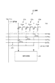
図7は、実施例1に係る画素回路を示す回路図であり、図中、図5と同等部位には同一符号を付して示している。
図7において、セレクタ部23の回路構成については、第1のスイッチ素子231及び第2のスイッチ素子232R,232G,232BがMOSトランジスタに置き換わっているだけであり、基本的な構成は、図5の場合と同じである。
次に、上記構成の実施例1に係る画素回路、即ち、副画素20R,20G,20Bの回路動作について、表示モード別に説明する。
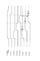
図8は、実施例1に係る画素回路のアナログ表示モードの動作説明に供するタイミング波形図である。図8には、(A)信号線31の電位、(B)制御信号GATE1、(C)赤色に対応した制御信号GATE2R、(D)緑色に対応した制御信号GATE2G、(E)青色に対応した制御信号GATE2B、及び、(F)制御信号SR1/SR2の各波形を示している。
メモリ表示モードでは、信号線31から階調を反映した信号電位を保持容量22R,22G,22Bに書き込む書き込み動作と、保持容量22R,22G,22Bの保持電位をリフレッシュするリフレッシュ動作とが行われる。このうち、書き込み動作は、表示内容を変更する場合等に実行される動作である。なお、信号線31から階調を反映した信号電位を保持容量22R,22G,22Bに書き込む動作については、アナログ表示モードの場合と同じであるので、ここではその説明を省略する。
図11は、実施例2に係る画素回路を示す回路図であり、図中、図7と同等部位には同一符号を付して示している。
図11において、セレクタ部23の回路構成については、実施例1の場合と全く同じである。すなわち、第1のスイッチングトランジスタ231は、一方の主電極(ドレイン電極/ソース電極)が信号線31に接続されている。そして、第1のスイッチングトランジスタ231は、制御信号GATE1による制御の下に、階調を反映した信号電位(Vsig/VXCS)を信号線31から画素20内に書き込む(取り込む)ときに導通状態となる。
次に、上記構成の実施例2に係る画素回路、即ち、副画素20R,20G,20Bの回路動作について、表示モード別に説明する。
図12は、実施例2に係る画素回路のアナログ表示モードの動作説明に供するタイミング波形図である。図12には、(A)信号線31の電位、(B)制御信号GATE1、(C)赤色に対応した制御信号GATE2R、(D)緑色に対応した制御信号GATE2G、(E)青色に対応した制御信号GATE2B、(F)制御信号SR1/SR2、及び、(G)制御信号SR3の各波形を示している。
メモリ表示モードでは、信号線31から階調を反映した信号電位を保持容量22R,22G,22Bに書き込む書き込み動作と、保持容量22R,22G,22Bの保持電位をリフレッシュするリフレッシュ動作とが行われる。このうち、書き込み動作は、表示内容を変更する場合等に実行される動作である。なお、信号線31から階調を反映した信号電位を保持容量22R,22G,22Bに書き込む動作については、アナログ表示モードの場合と同じであるので、ここではその説明を省略する。
上記実施形態では、3つの副画素20R,20G,20Bに対して1つの極性反転部24(24A,24B)を共通に設ける例について説明したが、これらは一例に過ぎず、画素内セレクタ方式を採る表示装置全般に適用可能である。従って、実施例で述べたような極性反転部については本発明においては必須ではないし、あるいは又、1つの極性反転部24を4つ以上の画素(副画素)間で共有する構成を採ること等も可能である。
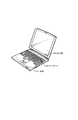
以上説明した本発明による液晶表示装置は、電子機器に入力された映像信号、または、電子機器内で生成した映像信号を、画像若しくは映像として表示するあらゆる分野の電子機器の表示装置に適用することが可能である。一例として、図15〜図19に示す様々な電子機器、例えば、デジタルカメラ、ノート型パーソナルコンピュータ、携帯電話等の携帯端末装置、ビデオカメラなどの表示装置に適用することが可能である。
Claims (8)
- 1つの画素を構成する複数の副画素に対して共通に設けられ、一端が信号線に接続された第1のスイッチ素子と、
前記複数の副画素毎に設けられ、各副画素の画素電極と前記第1のスイッチ素子の他端との間に接続された複数の第2のスイッチ素子と
が画素単位で配設されてなり、
前記第1のスイッチ素子のオン期間において前記複数の第2のスイッチ素子を順番にオン/オフ駆動するとともに、当該順番の最後にオン状態になる第2のスイッチ素子をオフ状態にした後、前記複数の第2のスイッチ素子の制御電極に付く寄生容量によるカップリングの条件が前記複数の副画素間で同じになるように、一定期間が経過してから前記第1のスイッチ素子をオフ状態にする駆動を行う駆動部を備え、
前記複数の副画素は、各々、前記第1のスイッチ素子及び前記複数の第2のスイッチ素子の各々を通して前記信号線から与えられる、階調を反映した信号電位を保持する容量素子を有する
液晶表示装置。 - 前記1つの画素は、前記複数の副画素に対して共通に設けられ、前記複数の副画素の各容量素子に保持された信号電位の極性を反転して前記容量素子に再度書き込む極性反転部を有する
請求項1に記載の液晶表示装置。 - 前記第1のスイッチ素子は、階調を反映した信号電位を前記容量素子に書き込む第1の動作モードではオン状態となり、前記容量素子から保持電位を読み出した後前記極性反転部で当該保持電位の極性を反転して前記容量素子に再度書き込む第2の動作モードではオフ状態となり、
前記複数の第2のスイッチ素子は、前記第1の動作モード、前記第2の動作モードにおける前記容量素子からの保持電位の読み出し期間、及び、前記極性反転部による反転電位の前記容量素子への再書き込み期間にオン状態となる
請求項2に記載の液晶表示装置。 - 前記極性反転部は、前記複数の副画素の各容量素子に保持された信号電位の極性を反転するインバータ回路を有する
請求項3に記載の液晶表示装置。 - 前記極性反転部は、前記複数の副画素の各容量素子に保持された信号電位の極性を反転し、当該反転電位を保持するラッチ回路を有する
請求項3に記載の液晶表示装置。 - 前記極性反転部は、
前記第1のスイッチ素子の他端と当該極性反転部の入力端との間に接続され、前記第1の動作モードではオフ状態となり、前記第2の動作モードにおける前記読み出し期間にオン状態となって前記容量素子から保持電位を前記複数の第2のスイッチ素子の各々を通じて読み出し、当該極性反転部の入力端に与える第3のスイッチ素子と、
前記第1のスイッチ素子の他端と当該極性反転部の出力端との間に接続され、前記第1の動作モードではオフ状態となり、前記第2の動作モードにおける前記再書き込み期間にオン状態となって当該極性反転部で極性反転された反転電位を前記複数の第2のスイッチ素子の各々を通じて前記容量素子に書き込む第4のスイッチ素子とを有する
請求項4または請求項5に記載の液晶表示装置。 - 1つの画素を構成する複数の副画素に対して共通に設けられ、一端が信号線に接続された第1のスイッチ素子と、
前記複数の副画素毎に設けられ、各副画素の画素電極と前記第1のスイッチ素子の他端との間に接続された複数の第2のスイッチ素子と
が画素単位で配線され、
前記複数の副画素は、各々、前記第1のスイッチ素子及び前記複数の第2のスイッチ素子の各々を通して前記信号線から与えられる、階調を反映した信号電位を保持する容量素子を有する液晶表示装置の駆動に当たって、
前記第1のスイッチ素子のオン期間において前記複数の第2のスイッチ素子を順番にオン/オフ駆動するとともに、当該順番の最後にオン状態になる第2のスイッチ素子をオフ状態にした後、前記複数の第2のスイッチ素子の制御電極に付く寄生容量によるカップリングの条件が前記複数の副画素間で同じになるように、一定期間が経過してから前記第1のスイッチ素子をオフ状態にする
液晶表示装置の駆動方法。 - 1つの画素を構成する複数の副画素に対して共通に設けられ、一端が信号線に接続された第1のスイッチ素子と、
前記複数の副画素毎に設けられ、各副画素の画素電極と前記第1のスイッチ素子の他端との間に接続された複数の第2のスイッチ素子と
が画素単位で配線されてなり、
前記第1のスイッチ素子のオン期間において前記複数の第2のスイッチ素子を順番にオン/オフ駆動するとともに、当該順番の最後にオン状態になる第2のスイッチ素子をオフ状態にした後、前記複数の第2のスイッチ素子の制御電極に付く寄生容量によるカップリングの条件が前記複数の副画素間で同じなるように、一定期間が経過してから前記第1のスイッチ素子をオフ状態にする駆動を行う駆動部を備え、
前記複数の副画素は、各々、前記第1のスイッチ素子及び前記複数の第2のスイッチ素子の各々を通して前記信号線から与えられる、階調を反映した信号電位を保持する容量素子を有する
液晶表示装置を有する電子機器。
Priority Applications (4)
| Application Number | Priority Date | Filing Date | Title |
|---|---|---|---|
| JP2010144152A JP5386441B2 (ja) | 2010-06-24 | 2010-06-24 | 液晶表示装置、液晶表示装置の駆動方法、及び、電子機器 |
| EP11167834A EP2400483A3 (en) | 2010-06-24 | 2011-05-27 | Liquid crystal display device, driving method of the same and electronic equipment |
| US13/159,617 US8947334B2 (en) | 2010-06-24 | 2011-06-14 | Liquid crystal display device including drive section for controlling timing of pixel switching elements, driving method of the same and electronic equipment |
| CN201110164468.0A CN102298914B (zh) | 2010-06-24 | 2011-06-17 | 液晶显示装置、其驱动方法以及电子设备 |
Applications Claiming Priority (1)
| Application Number | Priority Date | Filing Date | Title |
|---|---|---|---|
| JP2010144152A JP5386441B2 (ja) | 2010-06-24 | 2010-06-24 | 液晶表示装置、液晶表示装置の駆動方法、及び、電子機器 |
Publications (2)
| Publication Number | Publication Date |
|---|---|
| JP2012008339A JP2012008339A (ja) | 2012-01-12 |
| JP5386441B2 true JP5386441B2 (ja) | 2014-01-15 |
Family
ID=44675430
Family Applications (1)
| Application Number | Title | Priority Date | Filing Date |
|---|---|---|---|
| JP2010144152A Active JP5386441B2 (ja) | 2010-06-24 | 2010-06-24 | 液晶表示装置、液晶表示装置の駆動方法、及び、電子機器 |
Country Status (3)
| Country | Link |
|---|---|
| US (1) | US8947334B2 (ja) |
| EP (1) | EP2400483A3 (ja) |
| JP (1) | JP5386441B2 (ja) |
Families Citing this family (1)
| Publication number | Priority date | Publication date | Assignee | Title |
|---|---|---|---|---|
| JP2013050679A (ja) * | 2011-08-31 | 2013-03-14 | Sony Corp | 駆動回路、表示装置、および表示装置の駆動方法 |
Family Cites Families (16)
| Publication number | Priority date | Publication date | Assignee | Title |
|---|---|---|---|---|
| JPH04293015A (ja) * | 1991-03-22 | 1992-10-16 | Fujitsu Ltd | アクティブマトリックス液晶駆動回路 |
| JPH08146918A (ja) * | 1994-11-18 | 1996-06-07 | Sony Corp | スイッチング装置及びスイッチング方法 |
| JP3468986B2 (ja) * | 1996-04-16 | 2003-11-25 | 株式会社半導体エネルギー研究所 | アクティブマトリクス回路および表示装置 |
| US6414665B2 (en) * | 1998-11-04 | 2002-07-02 | International Business Machines Corporation | Multiplexing pixel circuits |
| US7230597B2 (en) * | 2001-07-13 | 2007-06-12 | Tpo Hong Kong Holding Limited | Active matrix array devices |
| US6897843B2 (en) * | 2001-07-14 | 2005-05-24 | Koninklijke Philips Electronics N.V. | Active matrix display devices |
| JP3603832B2 (ja) * | 2001-10-19 | 2004-12-22 | ソニー株式会社 | 液晶表示装置およびこれを用いた携帯端末装置 |
| JP4014895B2 (ja) * | 2001-11-28 | 2007-11-28 | 東芝松下ディスプレイテクノロジー株式会社 | 表示装置およびその駆動方法 |
| US20050157539A1 (en) * | 2002-05-10 | 2005-07-21 | Koninkliijke Philips Electronics N.V. | Memories and memory circuits |
| JP3758039B2 (ja) * | 2002-06-10 | 2006-03-22 | セイコーエプソン株式会社 | 駆動回路及び電気光学装置 |
| US7633472B2 (en) * | 2002-09-23 | 2009-12-15 | Chi Mei Optoelectronics Corporation | Active matrix display devices |
| US7940343B2 (en) | 2007-10-15 | 2011-05-10 | Sony Corporation | Liquid crystal display device and image displaying method of liquid crystal display device |
| JP5121386B2 (ja) | 2007-10-15 | 2013-01-16 | 株式会社ジャパンディスプレイウェスト | 液晶表示装置 |
| JP4752908B2 (ja) | 2008-12-17 | 2011-08-17 | ソニー株式会社 | 液晶表示パネル及び電子機器 |
| JP2010144152A (ja) | 2008-12-22 | 2010-07-01 | Nitto Denko Corp | 有機−無機複合成形体 |
| US8310638B2 (en) * | 2009-10-29 | 2012-11-13 | Sharp Kabushiki Kaisha | Pixel circuit and display apparatus |
-
2010
- 2010-06-24 JP JP2010144152A patent/JP5386441B2/ja active Active
-
2011
- 2011-05-27 EP EP11167834A patent/EP2400483A3/en not_active Ceased
- 2011-06-14 US US13/159,617 patent/US8947334B2/en active Active
Also Published As
| Publication number | Publication date |
|---|---|
| US8947334B2 (en) | 2015-02-03 |
| EP2400483A3 (en) | 2012-04-04 |
| US20110316819A1 (en) | 2011-12-29 |
| CN102298914A (zh) | 2011-12-28 |
| JP2012008339A (ja) | 2012-01-12 |
| EP2400483A2 (en) | 2011-12-28 |
Similar Documents
| Publication | Publication Date | Title |
|---|---|---|
| US9417495B2 (en) | Liquid crystal display panel and electronic device | |
| CN102298915B (zh) | 显示装置、用于驱动显示装置的方法以及电子设备 | |
| US6897843B2 (en) | Active matrix display devices | |
| US8294662B2 (en) | Electro-optical device, scan line driving circuit, and electronic apparatus | |
| CN100362563C (zh) | 平面显示装置 | |
| US20100073389A1 (en) | Display device | |
| JP2004309669A (ja) | アクティブマトリクス型表示装置とその駆動方法 | |
| CN103293729A (zh) | 液晶显示装置、驱动液晶显示装置的方法以及电子设备 | |
| KR100648141B1 (ko) | 표시 장치 및 상기 표시 장치의 구동 방법 | |
| JP5271383B2 (ja) | 液晶表示パネル及び電子機器 | |
| JP2009092787A (ja) | 表示装置、表示装置の駆動方法および電子機器 | |
| JP2008216893A (ja) | 平面表示装置及びその表示方法 | |
| JP2004109824A (ja) | 電気光学装置、電気光学装置の駆動方法、電気光学装置の駆動回路および電子機器 | |
| JP5495973B2 (ja) | 液晶表示装置、液晶表示装置の駆動方法、及び、電子機器 | |
| JP5386441B2 (ja) | 液晶表示装置、液晶表示装置の駆動方法、及び、電子機器 | |
| US7898516B2 (en) | Liquid crystal display device and mobile terminal | |
| US20060267902A1 (en) | Display device | |
| JP5495974B2 (ja) | 液晶表示装置、液晶表示装置の駆動方法、及び、電子機器 | |
| JP4508122B2 (ja) | 電気光学装置及び電子機器 | |
| JP2008096915A (ja) | 電気光学装置、走査線駆動回路および電子機器 | |
| CN102298914B (zh) | 液晶显示装置、其驱动方法以及电子设备 | |
| KR100879769B1 (ko) | 능동 매트릭스 어레이 장치 | |
| JP2003108099A (ja) | 表示装置 | |
| JP2009204868A (ja) | 液晶パネル、半導体デバイス、電子機器及び液晶パネルの駆動方法 | |
| JP2005308942A (ja) | 表示装置および表示装置の駆動方法 |
Legal Events
| Date | Code | Title | Description |
|---|---|---|---|
| A711 | Notification of change in applicant |
Free format text: JAPANESE INTERMEDIATE CODE: A711 Effective date: 20120330 |
|
| A621 | Written request for application examination |
Free format text: JAPANESE INTERMEDIATE CODE: A621 Effective date: 20130304 |
|
| RD03 | Notification of appointment of power of attorney |
Free format text: JAPANESE INTERMEDIATE CODE: A7423 Effective date: 20130328 |
|
| A977 | Report on retrieval |
Free format text: JAPANESE INTERMEDIATE CODE: A971007 Effective date: 20130619 |
|
| A131 | Notification of reasons for refusal |
Free format text: JAPANESE INTERMEDIATE CODE: A131 Effective date: 20130625 |
|
| A521 | Request for written amendment filed |
Free format text: JAPANESE INTERMEDIATE CODE: A523 Effective date: 20130820 |
|
| A711 | Notification of change in applicant |
Free format text: JAPANESE INTERMEDIATE CODE: A712 Effective date: 20130820 |
|
| TRDD | Decision of grant or rejection written | ||
| A01 | Written decision to grant a patent or to grant a registration (utility model) |
Free format text: JAPANESE INTERMEDIATE CODE: A01 Effective date: 20130910 |
|
| A61 | First payment of annual fees (during grant procedure) |
Free format text: JAPANESE INTERMEDIATE CODE: A61 Effective date: 20131007 |
|
| R150 | Certificate of patent or registration of utility model |
Free format text: JAPANESE INTERMEDIATE CODE: R150 Ref document number: 5386441 Country of ref document: JP Free format text: JAPANESE INTERMEDIATE CODE: R150 |
|
| R250 | Receipt of annual fees |
Free format text: JAPANESE INTERMEDIATE CODE: R250 |
|
| R250 | Receipt of annual fees |
Free format text: JAPANESE INTERMEDIATE CODE: R250 |
|
| R250 | Receipt of annual fees |
Free format text: JAPANESE INTERMEDIATE CODE: R250 |
|
| R250 | Receipt of annual fees |
Free format text: JAPANESE INTERMEDIATE CODE: R250 |
|
| R250 | Receipt of annual fees |
Free format text: JAPANESE INTERMEDIATE CODE: R250 |
|
| R250 | Receipt of annual fees |
Free format text: JAPANESE INTERMEDIATE CODE: R250 |
|
| R250 | Receipt of annual fees |
Free format text: JAPANESE INTERMEDIATE CODE: R250 |
|
| R250 | Receipt of annual fees |
Free format text: JAPANESE INTERMEDIATE CODE: R250 |
|
| R250 | Receipt of annual fees |
Free format text: JAPANESE INTERMEDIATE CODE: R250 |
|
| S111 | Request for change of ownership or part of ownership |
Free format text: JAPANESE INTERMEDIATE CODE: R313113 |
|
| R350 | Written notification of registration of transfer |
Free format text: JAPANESE INTERMEDIATE CODE: R350 |
|
| R250 | Receipt of annual fees |
Free format text: JAPANESE INTERMEDIATE CODE: R250 |