JP5398908B2 - 使用センサ - Google Patents
使用センサ Download PDFInfo
- Publication number
- JP5398908B2 JP5398908B2 JP2012512478A JP2012512478A JP5398908B2 JP 5398908 B2 JP5398908 B2 JP 5398908B2 JP 2012512478 A JP2012512478 A JP 2012512478A JP 2012512478 A JP2012512478 A JP 2012512478A JP 5398908 B2 JP5398908 B2 JP 5398908B2
- Authority
- JP
- Japan
- Prior art keywords
- functional layer
- thermal sensor
- processing stage
- battery
- sensor portion
- Prior art date
- Legal status (The legal status is an assumption and is not a legal conclusion. Google has not performed a legal analysis and makes no representation as to the accuracy of the status listed.)
- Expired - Fee Related
Links
- 239000002346 layers by function Substances 0.000 claims description 78
- 238000004519 manufacturing process Methods 0.000 claims description 39
- 238000012545 processing Methods 0.000 claims description 36
- 238000000034 method Methods 0.000 claims description 22
- 239000000463 material Substances 0.000 claims description 20
- 239000004065 semiconductor Substances 0.000 claims description 12
- XUIMIQQOPSSXEZ-UHFFFAOYSA-N Silicon Chemical compound [Si] XUIMIQQOPSSXEZ-UHFFFAOYSA-N 0.000 claims description 10
- 229910052710 silicon Inorganic materials 0.000 claims description 10
- 239000010703 silicon Substances 0.000 claims description 10
- 239000010410 layer Substances 0.000 description 21
- 238000013461 design Methods 0.000 description 19
- 239000011521 glass Substances 0.000 description 16
- 239000000758 substrate Substances 0.000 description 13
- 238000005530 etching Methods 0.000 description 9
- 230000008569 process Effects 0.000 description 9
- 230000005855 radiation Effects 0.000 description 8
- 239000000853 adhesive Substances 0.000 description 6
- 230000001070 adhesive effect Effects 0.000 description 6
- 230000008901 benefit Effects 0.000 description 4
- 229910021417 amorphous silicon Inorganic materials 0.000 description 3
- 239000000919 ceramic Substances 0.000 description 3
- 238000004891 communication Methods 0.000 description 3
- 238000012938 design process Methods 0.000 description 3
- 239000010408 film Substances 0.000 description 3
- 238000002955 isolation Methods 0.000 description 3
- 239000004642 Polyimide Substances 0.000 description 2
- 230000005540 biological transmission Effects 0.000 description 2
- 230000001419 dependent effect Effects 0.000 description 2
- 238000001514 detection method Methods 0.000 description 2
- 238000005516 engineering process Methods 0.000 description 2
- 238000004050 hot filament vapor deposition Methods 0.000 description 2
- 238000000623 plasma-assisted chemical vapour deposition Methods 0.000 description 2
- 229910021420 polycrystalline silicon Inorganic materials 0.000 description 2
- 229920001721 polyimide Polymers 0.000 description 2
- 239000007787 solid Substances 0.000 description 2
- 238000012876 topography Methods 0.000 description 2
- XHCLAFWTIXFWPH-UHFFFAOYSA-N [O-2].[O-2].[O-2].[O-2].[O-2].[V+5].[V+5] Chemical compound [O-2].[O-2].[O-2].[O-2].[O-2].[V+5].[V+5] XHCLAFWTIXFWPH-UHFFFAOYSA-N 0.000 description 1
- 239000006117 anti-reflective coating Substances 0.000 description 1
- 230000009286 beneficial effect Effects 0.000 description 1
- 230000007613 environmental effect Effects 0.000 description 1
- PCHJSUWPFVWCPO-UHFFFAOYSA-N gold Chemical compound [Au] PCHJSUWPFVWCPO-UHFFFAOYSA-N 0.000 description 1
- 239000010931 gold Substances 0.000 description 1
- 229910052737 gold Inorganic materials 0.000 description 1
- 238000009434 installation Methods 0.000 description 1
- 239000012212 insulator Substances 0.000 description 1
- 229910001386 lithium phosphate Inorganic materials 0.000 description 1
- 229910052751 metal Inorganic materials 0.000 description 1
- 239000002184 metal Substances 0.000 description 1
- 238000012986 modification Methods 0.000 description 1
- 230000004048 modification Effects 0.000 description 1
- 238000001020 plasma etching Methods 0.000 description 1
- 229920005591 polysilicon Polymers 0.000 description 1
- 230000001012 protector Effects 0.000 description 1
- 238000011160 research Methods 0.000 description 1
- 230000004044 response Effects 0.000 description 1
- 230000035945 sensitivity Effects 0.000 description 1
- 238000000926 separation method Methods 0.000 description 1
- 239000007784 solid electrolyte Substances 0.000 description 1
- 238000009987 spinning Methods 0.000 description 1
- 238000000992 sputter etching Methods 0.000 description 1
- 239000010409 thin film Substances 0.000 description 1
- 239000012780 transparent material Substances 0.000 description 1
- TWQULNDIKKJZPH-UHFFFAOYSA-K trilithium;phosphate Chemical compound [Li+].[Li+].[Li+].[O-]P([O-])([O-])=O TWQULNDIKKJZPH-UHFFFAOYSA-K 0.000 description 1
- 229910001935 vanadium oxide Inorganic materials 0.000 description 1
- 238000003631 wet chemical etching Methods 0.000 description 1
Images







Classifications
-
- H—ELECTRICITY
- H10—SEMICONDUCTOR DEVICES; ELECTRIC SOLID-STATE DEVICES NOT OTHERWISE PROVIDED FOR
- H10F—INORGANIC SEMICONDUCTOR DEVICES SENSITIVE TO INFRARED RADIATION, LIGHT, ELECTROMAGNETIC RADIATION OF SHORTER WAVELENGTH OR CORPUSCULAR RADIATION
- H10F30/00—Individual radiation-sensitive semiconductor devices in which radiation controls the flow of current through the devices, e.g. photodetectors
- H10F30/20—Individual radiation-sensitive semiconductor devices in which radiation controls the flow of current through the devices, e.g. photodetectors the devices having potential barriers, e.g. phototransistors
- H10F30/21—Individual radiation-sensitive semiconductor devices in which radiation controls the flow of current through the devices, e.g. photodetectors the devices having potential barriers, e.g. phototransistors the devices being sensitive to infrared, visible or ultraviolet radiation
-
- H—ELECTRICITY
- H05—ELECTRIC TECHNIQUES NOT OTHERWISE PROVIDED FOR
- H05B—ELECTRIC HEATING; ELECTRIC LIGHT SOURCES NOT OTHERWISE PROVIDED FOR; CIRCUIT ARRANGEMENTS FOR ELECTRIC LIGHT SOURCES, IN GENERAL
- H05B47/00—Circuit arrangements for operating light sources in general, i.e. where the type of light source is not relevant
- H05B47/10—Controlling the light source
- H05B47/105—Controlling the light source in response to determined parameters
- H05B47/115—Controlling the light source in response to determined parameters by determining the presence or movement of objects or living beings
-
- H—ELECTRICITY
- H10—SEMICONDUCTOR DEVICES; ELECTRIC SOLID-STATE DEVICES NOT OTHERWISE PROVIDED FOR
- H10F—INORGANIC SEMICONDUCTOR DEVICES SENSITIVE TO INFRARED RADIATION, LIGHT, ELECTROMAGNETIC RADIATION OF SHORTER WAVELENGTH OR CORPUSCULAR RADIATION
- H10F10/00—Individual photovoltaic cells, e.g. solar cells
-
- H—ELECTRICITY
- H10—SEMICONDUCTOR DEVICES; ELECTRIC SOLID-STATE DEVICES NOT OTHERWISE PROVIDED FOR
- H10F—INORGANIC SEMICONDUCTOR DEVICES SENSITIVE TO INFRARED RADIATION, LIGHT, ELECTROMAGNETIC RADIATION OF SHORTER WAVELENGTH OR CORPUSCULAR RADIATION
- H10F71/00—Manufacture or treatment of devices covered by this subclass
-
- H—ELECTRICITY
- H10—SEMICONDUCTOR DEVICES; ELECTRIC SOLID-STATE DEVICES NOT OTHERWISE PROVIDED FOR
- H10F—INORGANIC SEMICONDUCTOR DEVICES SENSITIVE TO INFRARED RADIATION, LIGHT, ELECTROMAGNETIC RADIATION OF SHORTER WAVELENGTH OR CORPUSCULAR RADIATION
- H10F77/00—Constructional details of devices covered by this subclass
- H10F77/95—Circuit arrangements
- H10F77/953—Circuit arrangements for devices having potential barriers
-
- Y—GENERAL TAGGING OF NEW TECHNOLOGICAL DEVELOPMENTS; GENERAL TAGGING OF CROSS-SECTIONAL TECHNOLOGIES SPANNING OVER SEVERAL SECTIONS OF THE IPC; TECHNICAL SUBJECTS COVERED BY FORMER USPC CROSS-REFERENCE ART COLLECTIONS [XRACs] AND DIGESTS
- Y02—TECHNOLOGIES OR APPLICATIONS FOR MITIGATION OR ADAPTATION AGAINST CLIMATE CHANGE
- Y02B—CLIMATE CHANGE MITIGATION TECHNOLOGIES RELATED TO BUILDINGS, e.g. HOUSING, HOUSE APPLIANCES OR RELATED END-USER APPLICATIONS
- Y02B20/00—Energy efficient lighting technologies, e.g. halogen lamps or gas discharge lamps
- Y02B20/40—Control techniques providing energy savings, e.g. smart controller or presence detection
-
- Y—GENERAL TAGGING OF NEW TECHNOLOGICAL DEVELOPMENTS; GENERAL TAGGING OF CROSS-SECTIONAL TECHNOLOGIES SPANNING OVER SEVERAL SECTIONS OF THE IPC; TECHNICAL SUBJECTS COVERED BY FORMER USPC CROSS-REFERENCE ART COLLECTIONS [XRACs] AND DIGESTS
- Y02—TECHNOLOGIES OR APPLICATIONS FOR MITIGATION OR ADAPTATION AGAINST CLIMATE CHANGE
- Y02E—REDUCTION OF GREENHOUSE GAS [GHG] EMISSIONS, RELATED TO ENERGY GENERATION, TRANSMISSION OR DISTRIBUTION
- Y02E10/00—Energy generation through renewable energy sources
- Y02E10/50—Photovoltaic [PV] energy
Landscapes
- Photovoltaic Devices (AREA)
- Photometry And Measurement Of Optical Pulse Characteristics (AREA)
- Investigating Or Analyzing Materials Using Thermal Means (AREA)
- Arrangements For Transmission Of Measured Signals (AREA)
Description
Claims (10)
- 熱センサ、バッテリ、アンテナ、電気回路及び太陽電池を一の半導体キャリアにおいて一体的に一緒に有するセンサデバイスを製造するための方法であって、
2つの対向する相互に平行な主表面をもつウェハー本体部をもつシリコンウェハーを設けるステップと、
第1の処理ステージにおいて、少なくとも1つの熱センサをもつ熱センサ部分を有する前記主表面の一方内又はその上に第1の機能層を作るとともに、前記熱センサ部分との非オーバーラップの関係で設けられた電気回路を有する第1の機能層を作るステップと、
前記第1の処理ステージの後の第2の処理ステージにおいて、前記熱センサ部分との非オーバーラップの関係で設けられるバッテリ及びアンテナを含む材料部分をもつ第2の機能層を作るステップと、
前記第1の処理ステージの後の第3の処理ステージにおいて、前記熱センサ部分との非オーバーラップの関係で設けられた1又はそれ以上の太陽電池を含む材料部分をもつ第3の機能層を作るステップと、
前記第3の処理ステージの後の第4の処理ステージにおいて、底面側から前記第1の機能層内の前記熱センサ部分に達する深さをもつ凹部をもたらすように、前記熱センサ部分の下の前記ウェハー本体部の部分が除去されるステップとを有し、
バッテリ及びアンテナをもつ前記第2の機能層は、前記第1の機能層上に作られ、太陽電池をもつ前記第3の機能層は、前記第2の機能層上に作られる、方法。 - 熱センサ、バッテリ、アンテナ、電気回路及び太陽電池を一の半導体キャリアにおいて一体的に一緒に有するセンサデバイスを製造するための方法であって、
2つの対向する相互に平行な主表面をもつウェハー本体部をもつシリコンウェハーを設けるステップと、
第1の処理ステージにおいて、少なくとも1つの熱センサをもつ熱センサ部分を有する前記主表面の一方内又はその上に第1の機能層を作るとともに、前記熱センサ部分との非オーバーラップの関係で設けられた電気回路を有する第1の機能層を作るステップと、
前記第1の処理ステージの後の第2の処理ステージにおいて、前記熱センサ部分との非オーバーラップの関係で設けられるバッテリ及びアンテナを含む材料部分をもつ第2の機能層を作るステップと、
前記第1の処理ステージの後の第3の処理ステージにおいて、前記熱センサ部分との非オーバーラップの関係で設けられた1又はそれ以上の太陽電池を含む材料部分をもつ第3の機能層を作るステップと、
前記第3の処理ステージの後の第4の処理ステージにおいて、底面側から前記第1の機能層内の前記熱センサ部分に達する深さをもつ凹部をもたらすように、前記熱センサ部分の下の前記ウェハー本体部の部分が除去されるステップとを有し、
バッテリ及びアンテナをもつ前記第2の機能層は、前記第1の機能層上に作られ、太陽電池をもつ前記第3の機能層は、前記主表面のうちの第2の主表面上に作られる、方法。 - 熱センサ、バッテリ、アンテナ、電気回路及び太陽電池を一の半導体キャリアにおいて一体的に一緒に有するセンサデバイスを製造するための方法であって、
2つの対向する相互に平行な主表面をもつウェハー本体部をもつシリコンウェハーを設けるステップと、
第1の処理ステージにおいて、少なくとも1つの熱センサをもつ熱センサ部分を有する前記主表面の一方内又はその上に第1の機能層を作るとともに、前記熱センサ部分との非オーバーラップの関係で設けられた電気回路を有する第1の機能層を作るステップと、
前記第1の処理ステージの後の第2の処理ステージにおいて、前記熱センサ部分との非オーバーラップの関係で設けられるバッテリ及びアンテナを含む材料部分をもつ第2の機能層を作るステップと、
前記第1の処理ステージの後の第3の処理ステージにおいて、前記熱センサ部分との非オーバーラップの関係で設けられた1又はそれ以上の太陽電池を含む材料部分をもつ第3の機能層を作るステップと、
前記第3の処理ステージの後の第4の処理ステージにおいて、底面側から前記第1の機能層内の前記熱センサ部分に達する深さをもつ凹部をもたらすように、前記熱センサ部分の下の前記ウェハー本体部の部分が除去されるステップとを有し、
バッテリ及びアンテナをもつ前記第2の機能層は、前記主表面のうちの第2の主表面上に作られ、太陽電池をもつ前記第3の機能層は、前記第1の機能層上に作られる、方法。 - 前記第2の機能層は、前記熱センサ部分と合わせられた空洞を有し、及び/又は、前記第3の機能層は、前記熱センサ部分と合わせられた空洞を有する、請求項1〜3のうちいずれか一項に記載の方法。
- 前記第2の機能層を製造するための製造プロセスは、400℃未満で実行される、請求項1〜3のうちいずれか一項に記載の方法。
- 前記第3の処理ステージは、前記第2の処理ステージの後に実行される、請求項1〜3のうちいずれか一項に記載の方法。
- 前記第3の機能層を製造するための製造プロセスは、300℃未満で実行される、請求項6に記載の方法。
- 請求項1〜7のうちいずれか一項に記載の方法により一の半導体本体において一体的に製造された熱センサ、バッテリ、アンテナ、電気回路及び太陽電池を有する、センサデバイス。
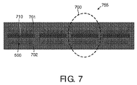
- 前記熱センサは、4つの個別センサ部分を有し、各センサ部分が、薄型中央長手本体部と前記中央本体部の対向する長手縁部に沿って設けられた複数の熱電対とを有する、請求項8に記載のセンサデバイス。
- 前記熱センサは、薄型中央長手本体部と、端部の熱電対に接触する端子及び中間の熱電対に接触する端子をもつ、前記中央本体部の対向する長手縁部に沿って設けられた複数の熱電対とを有し、従って、センサ信号は、前記センサの異なる部分から取得可能である、請求項8に記載のセンサデバイス。
Applications Claiming Priority (3)
| Application Number | Priority Date | Filing Date | Title |
|---|---|---|---|
| EP09161189.7 | 2009-05-27 | ||
| EP09161189 | 2009-05-27 | ||
| PCT/IB2010/052020 WO2010136919A1 (en) | 2009-05-27 | 2010-05-07 | Occupancy sensor |
Publications (2)
| Publication Number | Publication Date |
|---|---|
| JP2012528322A JP2012528322A (ja) | 2012-11-12 |
| JP5398908B2 true JP5398908B2 (ja) | 2014-01-29 |
Family
ID=42946153
Family Applications (1)
| Application Number | Title | Priority Date | Filing Date |
|---|---|---|---|
| JP2012512478A Expired - Fee Related JP5398908B2 (ja) | 2009-05-27 | 2010-05-07 | 使用センサ |
Country Status (8)
| Country | Link |
|---|---|
| US (1) | US8357550B2 (ja) |
| EP (1) | EP2436237B1 (ja) |
| JP (1) | JP5398908B2 (ja) |
| KR (1) | KR20120020186A (ja) |
| CN (1) | CN102450106B (ja) |
| CA (1) | CA2763240A1 (ja) |
| RU (1) | RU2011153187A (ja) |
| WO (1) | WO2010136919A1 (ja) |
Families Citing this family (16)
| Publication number | Priority date | Publication date | Assignee | Title |
|---|---|---|---|---|
| DE102010062559A1 (de) * | 2010-12-07 | 2012-06-14 | Robert Bosch Gmbh | Mikroelektromechanisches Sensormodul sowie entsprechendes Herstellungsverfahren |
| US8569861B2 (en) * | 2010-12-22 | 2013-10-29 | Analog Devices, Inc. | Vertically integrated systems |
| CN104011877A (zh) * | 2011-12-21 | 2014-08-27 | 陶氏环球技术有限责任公司 | 产生两个或更多个薄膜基互连光伏电池的改进方法 |
| US9871373B2 (en) | 2015-03-27 | 2018-01-16 | Analog Devices Global | Electrical overstress recording and/or harvesting |
| US10557881B2 (en) | 2015-03-27 | 2020-02-11 | Analog Devices Global | Electrical overstress reporting |
| KR20170089340A (ko) * | 2016-01-26 | 2017-08-03 | 엘지전자 주식회사 | 플렉서블 센서 모듈 및 이의 제조 방법 |
| US10338132B2 (en) | 2016-04-19 | 2019-07-02 | Analog Devices Global | Wear-out monitor device |
| US10365322B2 (en) | 2016-04-19 | 2019-07-30 | Analog Devices Global | Wear-out monitor device |
| DE102017011673A1 (de) * | 2016-12-21 | 2018-06-21 | Marquardt Gmbh | Sensorsystem mit einer Solarzelle |
| CN116124856B (zh) | 2017-05-15 | 2025-11-04 | 亚德诺半导体国际无限责任公司 | 集成离子传感设备和方法 |
| US11024525B2 (en) | 2017-06-12 | 2021-06-01 | Analog Devices International Unlimited Company | Diffusion temperature shock monitor |
| US10730743B2 (en) | 2017-11-06 | 2020-08-04 | Analog Devices Global Unlimited Company | Gas sensor packages |
| US11587839B2 (en) | 2019-06-27 | 2023-02-21 | Analog Devices, Inc. | Device with chemical reaction chamber |
| US10777611B1 (en) * | 2019-09-27 | 2020-09-15 | Sony Semiconductor Solutions Corporation | Image sensor |
| US12474290B2 (en) | 2019-11-20 | 2025-11-18 | Analog Devices International Unlimited Company | Electrochemical device |
| JP2021118551A (ja) * | 2020-01-22 | 2021-08-10 | ソニーセミコンダクタソリューションズ株式会社 | 撮像装置、センサ装置及び電子機器 |
Family Cites Families (18)
| Publication number | Priority date | Publication date | Assignee | Title |
|---|---|---|---|---|
| US10103A (en) * | 1853-10-11 | Detachable lining for the fire-boxes of steam-boilers | ||
| JPH08304174A (ja) * | 1995-04-28 | 1996-11-22 | Fujitsu Ltd | サーモパイル赤外線センサおよびセンサアレイ |
| JPH10242443A (ja) * | 1997-02-27 | 1998-09-11 | Toshiba Corp | 機能集積半導体装置 |
| DE10222499A1 (de) | 2002-05-22 | 2003-12-11 | Bosch Gmbh Robert | Verfahren zur Herstellung eines Bauteils, insbesondere eines thermischen Sensors, sowie thermischer Sensor |
| JP2004093535A (ja) * | 2002-09-04 | 2004-03-25 | Mitsubishi Electric Corp | 熱型赤外線固体撮像装置およびその製造方法 |
| US7868358B2 (en) * | 2003-06-06 | 2011-01-11 | Northrop Grumman Systems Corporation | Coiled circuit device with active circuitry and methods for making the same |
| JP2005106802A (ja) * | 2003-07-10 | 2005-04-21 | Canon Inc | 環境センサー、環境測定装置及び環境測定システム |
| EP1523043B1 (en) * | 2003-10-06 | 2011-12-28 | Semiconductor Energy Laboratory Co., Ltd. | Optical sensor and method for manufacturing the same |
| GB0408073D0 (en) | 2004-04-08 | 2004-05-12 | Council Cent Lab Res Councils | Optical sensor |
| WO2006132155A1 (ja) * | 2005-06-06 | 2006-12-14 | Matsushita Electric Industrial Co., Ltd. | 電子デバイス及びその製造方法 |
| US8173519B2 (en) * | 2006-03-03 | 2012-05-08 | Semiconductor Energy Laboratory Co., Ltd. | Method for manufacturing semiconductor device |
| JP2007280368A (ja) * | 2006-03-15 | 2007-10-25 | Semiconductor Energy Lab Co Ltd | 半導体装置及び当該半導体装置を具備するidラベル、idタグ、idカード |
| WO2007130471A2 (en) * | 2006-05-01 | 2007-11-15 | The Charles Stark Draper Laboratory, Inc. | Systems and methods for high density multi-component modules |
| US20070282210A1 (en) * | 2006-05-04 | 2007-12-06 | Stern David R | Implantable wireless sensor for in vivo pressure measurement and continuous output determination |
| US8459445B2 (en) * | 2006-07-21 | 2013-06-11 | Menicon, Co., Ltd. | Colored contact lens primary packaging |
| JP2008066402A (ja) * | 2006-09-05 | 2008-03-21 | Fujifilm Corp | 撮像素子および撮像装置 |
| JP5684475B2 (ja) | 2006-10-31 | 2015-03-11 | ソリコア インコーポレイテッドSOLICORE,Incorporated | 電池式デバイス |
| WO2009150562A1 (en) | 2008-06-11 | 2009-12-17 | Koninklijke Philips Electronics N.V. | Wireless sensor device and illumination system comprising such a device |
-
2010
- 2010-05-07 JP JP2012512478A patent/JP5398908B2/ja not_active Expired - Fee Related
- 2010-05-07 KR KR1020117031004A patent/KR20120020186A/ko not_active Withdrawn
- 2010-05-07 RU RU2011153187/07A patent/RU2011153187A/ru not_active Application Discontinuation
- 2010-05-07 US US13/322,296 patent/US8357550B2/en not_active Expired - Fee Related
- 2010-05-07 CA CA2763240A patent/CA2763240A1/en not_active Abandoned
- 2010-05-07 EP EP10719627A patent/EP2436237B1/en not_active Not-in-force
- 2010-05-07 WO PCT/IB2010/052020 patent/WO2010136919A1/en not_active Ceased
- 2010-05-07 CN CN201080023392.3A patent/CN102450106B/zh not_active Expired - Fee Related
Also Published As
| Publication number | Publication date |
|---|---|
| RU2011153187A (ru) | 2013-07-10 |
| CN102450106A (zh) | 2012-05-09 |
| EP2436237B1 (en) | 2012-12-26 |
| KR20120020186A (ko) | 2012-03-07 |
| WO2010136919A1 (en) | 2010-12-02 |
| CA2763240A1 (en) | 2010-12-02 |
| JP2012528322A (ja) | 2012-11-12 |
| EP2436237A1 (en) | 2012-04-04 |
| US20120077291A1 (en) | 2012-03-29 |
| US8357550B2 (en) | 2013-01-22 |
| CN102450106B (zh) | 2014-07-16 |
Similar Documents
| Publication | Publication Date | Title |
|---|---|---|
| JP5398908B2 (ja) | 使用センサ | |
| US8957488B2 (en) | Self powering application specific integrated circuit | |
| JP2011512689A5 (ja) | ||
| JP2021517731A (ja) | 薄膜太陽電池の直列接続構造及び薄膜太陽電池の直列接続構造の製造プロセス | |
| US9379265B2 (en) | Integrated circuit combination of a target integrated circuit, photovoltaic cells and light sensitive diodes connected to enable a self-sufficient light detector device | |
| JP2010500748A (ja) | 太陽電池複合体に一体化された薄膜電池 | |
| CN102437215A (zh) | 用于薄膜光伏器件的叠层内圆片层及薄膜光伏器件的制造方法 | |
| WO2011075967A1 (zh) | 搪瓷太阳能建筑墙板 | |
| CN103500768B (zh) | 一种柔性太阳能组件及其制作方法 | |
| US9905547B2 (en) | Chip with light energy harvester | |
| CN102017179A (zh) | 集成有微型联接装置的绝缘玻璃部件 | |
| KR101250207B1 (ko) | 다색 그림 태양전지 제조방법 | |
| WO2025175950A1 (zh) | 曲面光伏件 | |
| JPH0945946A (ja) | 太陽電池及びその製造方法 | |
| KR101294020B1 (ko) | 태양전지를 이용한 조명 장치 | |
| TW201327846A (zh) | 具有光轉向特徵之光電伏打窗 | |
| KR20080107181A (ko) | 고효율 태양전지 | |
| JP2015175816A (ja) | センサ端末装置 | |
| CN107863404A (zh) | 太阳能电池片及其制备方法、太阳能电池串以及光伏组件 | |
| US10170655B2 (en) | Energy harvesting device with prefabricated thin film energy absorption sheets and roll-to-sheet and roll-to-roll fabrication thereof | |
| CN108475042B (zh) | 具有太阳能指针的例如手表或测量仪器的便携式物体 | |
| JP4001260B2 (ja) | 太陽電池の製造方法および太陽電池 | |
| CN223037254U (zh) | 一种双色测温仪 | |
| JP3195011U (ja) | 建築資材 | |
| CN205159316U (zh) | 一种雪崩光电二极管的封装结构 |
Legal Events
| Date | Code | Title | Description |
|---|---|---|---|
| A621 | Written request for application examination |
Free format text: JAPANESE INTERMEDIATE CODE: A621 Effective date: 20130507 |
|
| A871 | Explanation of circumstances concerning accelerated examination |
Free format text: JAPANESE INTERMEDIATE CODE: A871 Effective date: 20130507 |
|
| A975 | Report on accelerated examination |
Free format text: JAPANESE INTERMEDIATE CODE: A971005 Effective date: 20130603 |
|
| A131 | Notification of reasons for refusal |
Free format text: JAPANESE INTERMEDIATE CODE: A131 Effective date: 20130606 |
|
| A521 | Request for written amendment filed |
Free format text: JAPANESE INTERMEDIATE CODE: A523 Effective date: 20130903 |
|
| TRDD | Decision of grant or rejection written | ||
| A01 | Written decision to grant a patent or to grant a registration (utility model) |
Free format text: JAPANESE INTERMEDIATE CODE: A01 Effective date: 20130926 |
|
| A61 | First payment of annual fees (during grant procedure) |
Free format text: JAPANESE INTERMEDIATE CODE: A61 Effective date: 20131022 |
|
| R150 | Certificate of patent or registration of utility model |
Free format text: JAPANESE INTERMEDIATE CODE: R150 |
|
| LAPS | Cancellation because of no payment of annual fees |