JP5418323B2 - Dielectric porcelain composition and electronic component - Google Patents
Dielectric porcelain composition and electronic component Download PDFInfo
- Publication number
- JP5418323B2 JP5418323B2 JP2010057662A JP2010057662A JP5418323B2 JP 5418323 B2 JP5418323 B2 JP 5418323B2 JP 2010057662 A JP2010057662 A JP 2010057662A JP 2010057662 A JP2010057662 A JP 2010057662A JP 5418323 B2 JP5418323 B2 JP 5418323B2
- Authority
- JP
- Japan
- Prior art keywords
- dielectric
- weight
- parts
- sample
- composition
- Prior art date
- Legal status (The legal status is an assumption and is not a legal conclusion. Google has not performed a legal analysis and makes no representation as to the accuracy of the status listed.)
- Active
Links
- 239000000203 mixture Substances 0.000 title claims description 78
- 229910052573 porcelain Inorganic materials 0.000 title claims description 5
- 239000000919 ceramic Substances 0.000 claims description 38
- AMWRITDGCCNYAT-UHFFFAOYSA-L hydroxy(oxo)manganese;manganese Chemical compound [Mn].O[Mn]=O.O[Mn]=O AMWRITDGCCNYAT-UHFFFAOYSA-L 0.000 claims description 26
- 229910000480 nickel oxide Inorganic materials 0.000 claims description 15
- 229910000420 cerium oxide Inorganic materials 0.000 claims description 13
- BMMGVYCKOGBVEV-UHFFFAOYSA-N oxo(oxoceriooxy)cerium Chemical compound [Ce]=O.O=[Ce]=O BMMGVYCKOGBVEV-UHFFFAOYSA-N 0.000 claims description 13
- GNRSAWUEBMWBQH-UHFFFAOYSA-N oxonickel Chemical compound [Ni]=O GNRSAWUEBMWBQH-UHFFFAOYSA-N 0.000 claims description 13
- 229910052791 calcium Inorganic materials 0.000 claims description 4
- 229910052749 magnesium Inorganic materials 0.000 claims description 4
- 229910052712 strontium Inorganic materials 0.000 claims description 4
- 239000003989 dielectric material Substances 0.000 claims 2
- WPBNNNQJVZRUHP-UHFFFAOYSA-L manganese(2+);methyl n-[[2-(methoxycarbonylcarbamothioylamino)phenyl]carbamothioyl]carbamate;n-[2-(sulfidocarbothioylamino)ethyl]carbamodithioate Chemical compound [Mn+2].[S-]C(=S)NCCNC([S-])=S.COC(=O)NC(=S)NC1=CC=CC=C1NC(=S)NC(=O)OC WPBNNNQJVZRUHP-UHFFFAOYSA-L 0.000 claims 1
- 230000015556 catabolic process Effects 0.000 description 23
- 239000010410 layer Substances 0.000 description 19
- 239000003985 ceramic capacitor Substances 0.000 description 18
- 239000003990 capacitor Substances 0.000 description 17
- 239000002994 raw material Substances 0.000 description 17
- 239000000843 powder Substances 0.000 description 12
- 230000007423 decrease Effects 0.000 description 8
- 238000000034 method Methods 0.000 description 8
- 239000011575 calcium Substances 0.000 description 7
- 238000010304 firing Methods 0.000 description 7
- 230000020169 heat generation Effects 0.000 description 7
- 230000005684 electric field Effects 0.000 description 6
- 238000004519 manufacturing process Methods 0.000 description 6
- 238000001354 calcination Methods 0.000 description 5
- 239000011777 magnesium Substances 0.000 description 5
- 239000010936 titanium Substances 0.000 description 5
- 239000002131 composite material Substances 0.000 description 3
- 238000005259 measurement Methods 0.000 description 3
- 230000001681 protective effect Effects 0.000 description 3
- 239000011347 resin Substances 0.000 description 3
- 229920005989 resin Polymers 0.000 description 3
- VTYYLEPIZMXCLO-UHFFFAOYSA-L Calcium carbonate Chemical compound [Ca+2].[O-]C([O-])=O VTYYLEPIZMXCLO-UHFFFAOYSA-L 0.000 description 2
- 239000004372 Polyvinyl alcohol Substances 0.000 description 2
- MCMNRKCIXSYSNV-UHFFFAOYSA-N Zirconium dioxide Chemical compound O=[Zr]=O MCMNRKCIXSYSNV-UHFFFAOYSA-N 0.000 description 2
- JRPBQTZRNDNNOP-UHFFFAOYSA-N barium titanate Chemical compound [Ba+2].[Ba+2].[O-][Ti]([O-])([O-])[O-] JRPBQTZRNDNNOP-UHFFFAOYSA-N 0.000 description 2
- 229910002113 barium titanate Inorganic materials 0.000 description 2
- 239000011230 binding agent Substances 0.000 description 2
- 150000001875 compounds Chemical class 0.000 description 2
- 239000004020 conductor Substances 0.000 description 2
- 230000003247 decreasing effect Effects 0.000 description 2
- 238000005516 engineering process Methods 0.000 description 2
- 150000004679 hydroxides Chemical class 0.000 description 2
- 229920002451 polyvinyl alcohol Polymers 0.000 description 2
- 238000007639 printing Methods 0.000 description 2
- 229910052709 silver Inorganic materials 0.000 description 2
- 238000010532 solid phase synthesis reaction Methods 0.000 description 2
- 229910001316 Ag alloy Inorganic materials 0.000 description 1
- 229910018072 Al 2 O 3 Inorganic materials 0.000 description 1
- 229910000881 Cu alloy Inorganic materials 0.000 description 1
- 229910000807 Ga alloy Inorganic materials 0.000 description 1
- 101100513612 Microdochium nivale MnCO gene Proteins 0.000 description 1
- MUBZPKHOEPUJKR-UHFFFAOYSA-N Oxalic acid Chemical compound OC(=O)C(O)=O MUBZPKHOEPUJKR-UHFFFAOYSA-N 0.000 description 1
- BQCADISMDOOEFD-UHFFFAOYSA-N Silver Chemical compound [Ag] BQCADISMDOOEFD-UHFFFAOYSA-N 0.000 description 1
- 229910010413 TiO 2 Inorganic materials 0.000 description 1
- GWEVSGVZZGPLCZ-UHFFFAOYSA-N Titan oxide Chemical compound O=[Ti]=O GWEVSGVZZGPLCZ-UHFFFAOYSA-N 0.000 description 1
- 229910052788 barium Inorganic materials 0.000 description 1
- AYJRCSIUFZENHW-UHFFFAOYSA-L barium carbonate Chemical compound [Ba+2].[O-]C([O-])=O AYJRCSIUFZENHW-UHFFFAOYSA-L 0.000 description 1
- 229910000019 calcium carbonate Inorganic materials 0.000 description 1
- 150000004649 carbonic acid derivatives Chemical class 0.000 description 1
- 238000006243 chemical reaction Methods 0.000 description 1
- 229910052802 copper Inorganic materials 0.000 description 1
- 230000018044 dehydration Effects 0.000 description 1
- 238000006297 dehydration reaction Methods 0.000 description 1
- 238000001035 drying Methods 0.000 description 1
- 239000002003 electrode paste Substances 0.000 description 1
- 230000002349 favourable effect Effects 0.000 description 1
- 238000001027 hydrothermal synthesis Methods 0.000 description 1
- BDAGIHXWWSANSR-NJFSPNSNSA-N hydroxyformaldehyde Chemical compound O[14CH]=O BDAGIHXWWSANSR-NJFSPNSNSA-N 0.000 description 1
- 238000011835 investigation Methods 0.000 description 1
- WABPQHHGFIMREM-UHFFFAOYSA-N lead(0) Chemical compound [Pb] WABPQHHGFIMREM-UHFFFAOYSA-N 0.000 description 1
- 239000007791 liquid phase Substances 0.000 description 1
- ZLNQQNXFFQJAID-UHFFFAOYSA-L magnesium carbonate Chemical compound [Mg+2].[O-]C([O-])=O ZLNQQNXFFQJAID-UHFFFAOYSA-L 0.000 description 1
- 229910052751 metal Inorganic materials 0.000 description 1
- 150000002736 metal compounds Chemical class 0.000 description 1
- 238000002156 mixing Methods 0.000 description 1
- 150000002823 nitrates Chemical class 0.000 description 1
- RVTZCBVAJQQJTK-UHFFFAOYSA-N oxygen(2-);zirconium(4+) Chemical compound [O-2].[O-2].[Zr+4] RVTZCBVAJQQJTK-UHFFFAOYSA-N 0.000 description 1
- 230000002250 progressing effect Effects 0.000 description 1
- 238000010298 pulverizing process Methods 0.000 description 1
- 239000004332 silver Substances 0.000 description 1
- 239000002356 single layer Substances 0.000 description 1
- 238000005476 soldering Methods 0.000 description 1
- 229910000018 strontium carbonate Inorganic materials 0.000 description 1
- 239000000758 substrate Substances 0.000 description 1
- 229910052719 titanium Inorganic materials 0.000 description 1
- 150000003609 titanium compounds Chemical class 0.000 description 1
- 238000005303 weighing Methods 0.000 description 1
- 229910052726 zirconium Inorganic materials 0.000 description 1
- 229910001928 zirconium oxide Inorganic materials 0.000 description 1
Images


Classifications
-
- H—ELECTRICITY
- H01—ELECTRIC ELEMENTS
- H01G—CAPACITORS; CAPACITORS, RECTIFIERS, DETECTORS, SWITCHING DEVICES, LIGHT-SENSITIVE OR TEMPERATURE-SENSITIVE DEVICES OF THE ELECTROLYTIC TYPE
- H01G4/00—Fixed capacitors; Processes of their manufacture
- H01G4/002—Details
- H01G4/018—Dielectrics
- H01G4/06—Solid dielectrics
- H01G4/08—Inorganic dielectrics
- H01G4/12—Ceramic dielectrics
- H01G4/1209—Ceramic dielectrics characterised by the ceramic dielectric material
- H01G4/1218—Ceramic dielectrics characterised by the ceramic dielectric material based on titanium oxides or titanates
- H01G4/1227—Ceramic dielectrics characterised by the ceramic dielectric material based on titanium oxides or titanates based on alkaline earth titanates
-
- C—CHEMISTRY; METALLURGY
- C01—INORGANIC CHEMISTRY
- C01G—COMPOUNDS CONTAINING METALS NOT COVERED BY SUBCLASSES C01D OR C01F
- C01G45/00—Compounds of manganese
- C01G45/02—Oxides
-
- C—CHEMISTRY; METALLURGY
- C01—INORGANIC CHEMISTRY
- C01G—COMPOUNDS CONTAINING METALS NOT COVERED BY SUBCLASSES C01D OR C01F
- C01G53/00—Compounds of nickel
- C01G53/04—Oxides
-
- C—CHEMISTRY; METALLURGY
- C04—CEMENTS; CONCRETE; ARTIFICIAL STONE; CERAMICS; REFRACTORIES
- C04B—LIME, MAGNESIA; SLAG; CEMENTS; COMPOSITIONS THEREOF, e.g. MORTARS, CONCRETE OR LIKE BUILDING MATERIALS; ARTIFICIAL STONE; CERAMICS; REFRACTORIES; TREATMENT OF NATURAL STONE
- C04B35/00—Shaped ceramic products characterised by their composition; Ceramics compositions; Processing powders of inorganic compounds preparatory to the manufacturing of ceramic products
- C04B35/01—Shaped ceramic products characterised by their composition; Ceramics compositions; Processing powders of inorganic compounds preparatory to the manufacturing of ceramic products based on oxide ceramics
- C04B35/46—Shaped ceramic products characterised by their composition; Ceramics compositions; Processing powders of inorganic compounds preparatory to the manufacturing of ceramic products based on oxide ceramics based on titanium oxides or titanates
- C04B35/462—Shaped ceramic products characterised by their composition; Ceramics compositions; Processing powders of inorganic compounds preparatory to the manufacturing of ceramic products based on oxide ceramics based on titanium oxides or titanates based on titanates
- C04B35/465—Shaped ceramic products characterised by their composition; Ceramics compositions; Processing powders of inorganic compounds preparatory to the manufacturing of ceramic products based on oxide ceramics based on titanium oxides or titanates based on titanates based on alkaline earth metal titanates
Landscapes
- Chemical & Material Sciences (AREA)
- Engineering & Computer Science (AREA)
- Organic Chemistry (AREA)
- Ceramic Engineering (AREA)
- Inorganic Chemistry (AREA)
- Power Engineering (AREA)
- Manufacturing & Machinery (AREA)
- Microelectronics & Electronic Packaging (AREA)
- Materials Engineering (AREA)
- Structural Engineering (AREA)
- Compositions Of Oxide Ceramics (AREA)
- Inorganic Insulating Materials (AREA)
- Ceramic Capacitors (AREA)
Description
本発明は、誘電体磁器組成物および電子部品に関する。 The present invention relates to a dielectric ceramic composition and an electronic component.
近年、急速に進む電気機器の高性能化に伴い、電気回路の小型化、複雑化もまた急速に進んでいる。そのため、電子部品にもより一層の小型化、高性能化が求められている。すなわち、良好な温度特性を維持しつつ、小型化しても静電容量を維持するために比誘電率が高く、さらに高電圧下で使用するために交流破壊電圧が高い誘電体磁器組成物および電子部品が求められている。 In recent years, along with rapid progress in performance of electrical equipment, miniaturization and complexity of electrical circuits are also progressing rapidly. For this reason, electronic components are required to be further reduced in size and performance. That is, a dielectric ceramic composition and an electron having a high relative dielectric constant in order to maintain capacitance even when miniaturized while maintaining good temperature characteristics, and also having a high AC breakdown voltage for use under a high voltage Parts are required.
従来、磁器コンデンサ、積層コンデンサ、高周波用コンデンサ、高電圧用コンデンサ等として広く利用されている高誘電率誘電体磁器組成物として、特許文献1に示すものが知られている。この特許文献1には、組成式が(Ba1−xCax)(Ti1−yZry)O3(但し、0.10<x≦0.25、0<y≦0.25)で表されるチタン酸バリウムを主成分とする誘電体磁器組成物が開示されている。
Conventionally, as a high dielectric constant dielectric ceramic composition widely used as a ceramic capacitor, a multilayer capacitor, a high frequency capacitor, a high voltage capacitor or the like, the one shown in
また、特許文献2には、組成式が(Ba1−xCax)(Ti1−yZry)O3(但し、0<x≦0.25、0<y≦0.25)で表される、チタン酸バリウムを主成分とし、さらにY2O3、MgO、Al2O3を含有する誘電体磁器組成物が開示されている。
In
しかし、このような従来の高誘電率誘電体磁器組成物では、比誘電率を3000以上とした場合に、誘電損失を低減することが困難であるとともに、6kV/mm以上の高い交流破壊電圧を確保することが困難であった。 However, in such a conventional high dielectric constant dielectric ceramic composition, when the relative dielectric constant is 3000 or more, it is difficult to reduce the dielectric loss, and a high AC breakdown voltage of 6 kV / mm or more is required. It was difficult to secure.
本発明は、このような実状に鑑みてなされ、その目的は、比誘電率および交流破壊電圧が高く、誘電損失が低く、温度特性および焼結性が良好な誘電体磁器組成物を提供することを目的とする。また、本発明は、このような誘電体磁器組成物により構成される誘電体層を有する電子部品を提供することも目的とする。 The present invention has been made in view of such circumstances, and its object is to provide a dielectric ceramic composition having a high relative dielectric constant and AC breakdown voltage, low dielectric loss, and good temperature characteristics and sinterability. With the goal. Another object of the present invention is to provide an electronic component having a dielectric layer composed of such a dielectric ceramic composition.
本発明者等は、上記目的を達成するために、鋭意検討を行った結果、誘電体磁器組成物の組成を特定の成分とし、これらの比率を所定範囲とすることにより、上記目的を達成できることを見出し、本発明を完成させるに至った。 As a result of intensive investigations to achieve the above object, the present inventors are able to achieve the above object by setting the composition of the dielectric ceramic composition as a specific component and setting these ratios within a predetermined range. As a result, the present invention has been completed.
すなわち、上記課題を解決する本発明に係る誘電体磁器組成物は、(Ba1−u−v−w,Cau,Mgv,Srw)α(Ti1−x,Zrx)O3 の組成式で表わされる主成分と、酸化ニッケルと、酸化セリウムと、酸化マンガンと、を有する誘電体磁器組成物であって、
前記組成式中のuが0.20〜0.27であり、
前記組成式中のvが0.018〜0.049であり、
前記組成式中のwが0.004〜0.018であり、
前記組成式中のxが0.118〜0.149であり、
前記組成式中のαが0.95〜1.02であり、
前記酸化ニッケルを前記主成分100重量部に対して0.03〜0.4重量部含有し、
前記酸化セリウムを前記主成分100重量部に対して0.03〜0.4重量部含有し、
前記酸化マンガンを前記主成分100重量部に対して0.03〜0.4重量部含有する誘電体磁器組成物である。
That is, the dielectric ceramic composition according to the present invention for solving the aforementioned problems is, (Ba 1-u-v -w, Ca u, Mg v, Sr w) α (Ti 1-x, Zr x) of O 3 A dielectric ceramic composition having a main component represented by a composition formula, nickel oxide, cerium oxide, and manganese oxide,
U in the composition formula is 0.20 to 0.27,
V in the composition formula is 0.018 to 0.049,
W in the composition formula is 0.004 to 0.018,
X in the composition formula is 0.118 to 0.149,
Α in the composition formula is 0.95 to 1.02,
Containing 0.03 to 0.4 parts by weight of the nickel oxide with respect to 100 parts by weight of the main component,
Containing 0.03 to 0.4 parts by weight of the cerium oxide with respect to 100 parts by weight of the main component,
The dielectric ceramic composition contains 0.03 to 0.4 parts by weight of the manganese oxide with respect to 100 parts by weight of the main component.
本発明によれば、比誘電率および交流破壊電圧が高く、誘電損失が低く、温度特性および焼結性が良好な誘電体磁器組成物を提供することができる。また、本発明によれば、室温における熱暴走を防ぐことができる誘電体磁器組成物を提供することができる。具体的には、誘電体磁器組成物のキュリー温度を20℃以下にすることで室温における熱暴走を防ぐことができる。 According to the present invention, it is possible to provide a dielectric ceramic composition having a high relative dielectric constant and AC breakdown voltage, low dielectric loss, and good temperature characteristics and sinterability. Moreover, according to this invention, the dielectric ceramic composition which can prevent the thermal runaway at room temperature can be provided. Specifically, thermal runaway at room temperature can be prevented by setting the Curie temperature of the dielectric ceramic composition to 20 ° C. or lower.
ここで、熱暴走とは発熱が更なる発熱を招くという正のフィードバックにより、温度の制御が出来なくなる現象である。 Here, thermal runaway is a phenomenon in which the temperature cannot be controlled due to positive feedback that heat generation causes further heat generation.
本発明の実施形態に係る電子部品は、前記誘電体磁器組成物で構成してある誘電体層を有する。 An electronic component according to an embodiment of the present invention has a dielectric layer made of the dielectric ceramic composition.
本発明の実施形態に係る電子部品としては、特に限定されないが、単板型セラミックコンデンサ、貫通型コンデンサ、積層セラミックコンデンサ、圧電素子、チップインダクタ、チップバリスタ、チップサーミスタ、チップ抵抗、その他の表面実装(SMD)チップ型電子部品が例示される。 The electronic component according to the embodiment of the present invention is not particularly limited, but includes a single plate type ceramic capacitor, a feedthrough capacitor, a multilayer ceramic capacitor, a piezoelectric element, a chip inductor, a chip varistor, a chip thermistor, a chip resistor, and other surface mounts. (SMD) chip type electronic components are exemplified.
以下、本発明の実施形態を、図面に示す実施形態に基づき説明する。 DESCRIPTION OF EMBODIMENTS Hereinafter, embodiments of the present invention will be described based on the embodiments shown in the drawings.
セラミックコンデンサ2
図1(A)に示すように、本発明の実施形態に係るセラミックコンデンサ2は、誘電体層10と、その対向表面に形成された一対の端子電極12,14と、この端子電極12,14に、それぞれ接続されたリード端子6,8とを有する構成となっており、これらは保護樹脂4に覆われている。セラミックコンデンサ2の形状は、目的や用途に応じて適宜決定すればよいが、誘電体層10が円板形状となっている円板型のコンデンサであることが好ましい。また、そのサイズは、目的や用途に応じて適宜決定すればよいが、通常、直径が5〜20mm程度、好ましくは5〜15mm程度である。
As shown in FIG. 1A, a
誘電体層10の厚みは、特に限定されず、用途等に応じて適宜決定すれば良いが、好ましくは0.3〜2mmである。誘電体層10の厚みを、このような範囲とすることにより、中高圧用途に好適に用いることができる。
The thickness of the
端子電極12,14は、導電材で構成される。端子電極12,14に用いられる導電材としては、たとえば、Cu、Cu合金、Ag、Ag合金、In−Ga合金等が挙げられる。
The
誘電体層10
前記セラミックコンデンサ2の誘電体層10は、本発明の実施形態に係る誘電体磁器組成物により構成される。
The
本発明の実施形態に係る誘電体磁器組成物は、(Ba1−u−v−w,Cau,Mgv,Srw)α(Ti1−x,Zrx)O3 の組成式で表わされる主成分と、酸化ニッケルと、酸化セリウムと、酸化マンガンと、を有する誘電体磁器組成物である。 The dielectric ceramic composition according to an embodiment of the present invention is represented by a composition formula of (Ba 1-u-v- w, Ca u, Mg v, Sr w) α (Ti 1-x, Zr x) O 3 A dielectric ceramic composition having a main component, nickel oxide, cerium oxide, and manganese oxide.
前記組成式中のuは、Caの比率を表し、その範囲は0.20〜0.27、好ましくは0.22〜0.24である。Caがこの範囲で含有されることにより、比誘電率が向上し、誘電損失が低下し、温度特性が良好になる傾向となる。 U in the composition formula represents the ratio of Ca, and the range thereof is 0.20 to 0.27, preferably 0.22 to 0.24. When Ca is contained in this range, the relative dielectric constant is improved, the dielectric loss is lowered, and the temperature characteristics tend to be improved.
前記組成式中のvは、Mgの比率を表し、その範囲は0.018〜0.049、好ましくは0.028〜0.03である。Mgがこの範囲で含有されることにより、比誘電率、交流破壊電圧および焼結性が向上し、温度特性が良好になる傾向となる。 V in the composition formula represents a ratio of Mg, and the range thereof is 0.018 to 0.049, preferably 0.028 to 0.03. By containing Mg in this range, the relative permittivity, the AC breakdown voltage and the sinterability are improved, and the temperature characteristics tend to be good.
前記組成式中のwは、Srの比率を表し、その範囲は0.004〜0.018、好ましくは0.015〜0.017である。Srがこの範囲で含有されることにより、温度特性が良好となり、誘電損失が低下する傾向となる。 W in the composition formula represents a ratio of Sr, and the range thereof is 0.004 to 0.018, preferably 0.015 to 0.017. When Sr is contained in this range, the temperature characteristics are improved and the dielectric loss tends to decrease.
前記組成式中のxは、Zrの比率を表し、その範囲は0.118〜0.149、好ましくは0.13〜0.14である。Zrがこの範囲で含有されることにより、誘電損失が低下し、交流破壊電圧が向上し、温度特性が良好になる傾向となる。 X in the composition formula represents a ratio of Zr, and the range thereof is 0.118 to 0.149, preferably 0.13 to 0.14. When Zr is contained in this range, the dielectric loss is reduced, the AC breakdown voltage is improved, and the temperature characteristics tend to be improved.
前記組成式中のαは、0.95〜1.02であり、より好ましくは1.01〜1.015である。αをこの範囲とすることにより、比誘電率および焼結性が向上し、誘電損失およびキュリー温度が低下する傾向となる。 Α in the composition formula is 0.95 to 1.02, more preferably 1.01 to 1.015. By setting α within this range, the relative permittivity and sinterability are improved, and the dielectric loss and the Curie temperature tend to decrease.
本発明の実施形態に係る誘電体磁器組成物は、酸化ニッケルを前記主成分100重量部に対して0.03〜0.4重量部含有し、好ましくは0.05〜0.3重量部、より好ましくは、0.1〜0.2重量部重量部含有する。酸化ニッケルがこの範囲で含有されることにより、比誘電率、交流破壊電圧および焼結性が向上する傾向となる。 The dielectric ceramic composition according to the embodiment of the present invention contains 0.03 to 0.4 parts by weight, preferably 0.05 to 0.3 parts by weight of nickel oxide based on 100 parts by weight of the main component. More preferably, it contains 0.1 to 0.2 parts by weight. By containing nickel oxide in this range, the relative permittivity, the AC breakdown voltage, and the sinterability tend to be improved.
本発明の実施形態に係る誘電体磁器組成物は、酸化セリウムを前記主成分100重量部に対して0.03〜0.4重量部含有し、好ましくは0.05〜0.3重量部、より好ましくは、0.1〜0.2重量部含有する。酸化セリウムがこの範囲で含有されることにより、温度特性が良好となり、交流破壊電圧および比誘電率が向上し、誘電損失が低下する傾向となる。 The dielectric ceramic composition according to the embodiment of the present invention contains 0.03 to 0.4 parts by weight, preferably 0.05 to 0.3 parts by weight, of cerium oxide with respect to 100 parts by weight of the main component. More preferably, it contains 0.1 to 0.2 parts by weight. By containing cerium oxide in this range, the temperature characteristics are improved, the AC breakdown voltage and the relative dielectric constant are improved, and the dielectric loss tends to decrease.
本発明の実施形態に係る誘電体磁器組成物は、酸化マンガンを前記主成分100重量部に対して0.03〜0.4重量部含有し、好ましくは0.05〜0.3重量部、より好ましくは、0.1〜0.2重量部含有する。酸化マンガンがこの範囲で含有されることにより、比誘電率、交流破壊電圧および焼結性が向上し、誘電損失が低下する傾向となる。 The dielectric ceramic composition according to the embodiment of the present invention contains 0.03 to 0.4 parts by weight, preferably 0.05 to 0.3 parts by weight of manganese oxide with respect to 100 parts by weight of the main component. More preferably, it contains 0.1 to 0.2 parts by weight. By containing manganese oxide in this range, the relative dielectric constant, the AC breakdown voltage, and the sinterability are improved, and the dielectric loss tends to decrease.
以下では酸化ニッケル、酸化セリウムまたは酸化マンガンを「副成分」とする。 Hereinafter, nickel oxide, cerium oxide or manganese oxide is referred to as “subcomponent”.
セラミックコンデンサ2の製造方法
次に、セラミックコンデンサ2の製造方法について説明する。
まず、焼成後に図1に示す誘電体層10を形成することとなる誘電体磁器組成物粉末を製造する。
Manufacturing method of
Next, a method for manufacturing the
First, a dielectric ceramic composition powder that will form the
主成分の原料および各副成分の原料を準備する。主成分の原料としては、Ba、Ca、Mg、Sr、Ti、Zrの各酸化物および/または焼成により酸化物となる原料や、これらの複合酸化物などが挙げられ、たとえば、炭酸バリウム(BaCO3 )、炭酸カルシウム(CaCO3 )、炭酸マグネシウム(MgCO3 )、炭酸ストロンチウム(SrCO3 )、酸化チタン(TiO2 )、酸化ジルコニウム(ZrO2 )、酸化ニッケル(NiO)、酸化セリウム(CeO2 )、酸化マンガン(MnO)などを用いることができる。この他、たとえば水酸化物など、焼成後に酸化物やチタン化合物となる種々の化合物を用いることも可能である。その場合、金属元素の元素数が合うように、含有量を適宜変更すればよい。 A raw material for the main component and a raw material for each subcomponent are prepared. Examples of the main component raw material include Ba, Ca, Mg, Sr, Ti, and Zr oxides and / or raw materials that become oxides by firing, and composite oxides thereof. For example, barium carbonate (BaCO 3 ), calcium carbonate (CaCO 3 ), magnesium carbonate (MgCO 3 ), strontium carbonate (SrCO 3 ), titanium oxide (TiO 2 ), zirconium oxide (ZrO 2 ), nickel oxide (NiO), cerium oxide (CeO 2 ) Manganese oxide (MnO) or the like can be used. In addition, it is also possible to use various compounds that become oxides or titanium compounds after firing, such as hydroxides. In that case, the content may be changed as appropriate so that the number of metal elements matches.
また、主成分の原料は、固相法により製造してもよいし、水熱合成法や蓚酸塩法などの液相法により製造してもよいが、製造コストの面から、固相法により製造することが好ましい。 The main component raw material may be manufactured by a solid phase method or a liquid phase method such as a hydrothermal synthesis method or an oxalate method. It is preferable to manufacture.
各副成分の原料としては、特に限定されず、上記した各副成分の酸化物や複合酸化物、または焼成によりこれら酸化物や複合酸化物となる各種化合物、たとえば炭酸塩、硝酸塩、水酸化物、有機金属化合物などから適宜選択して用いることができる。 The raw materials for each subcomponent are not particularly limited, and the above-mentioned oxides and composite oxides of each subcomponent, or various compounds that become these oxides or composite oxides by firing, such as carbonates, nitrates, hydroxides, etc. , Organic metal compounds and the like can be appropriately selected and used.
本発明の実施形態に係る誘電体磁器組成物の製造方法としては、まず主成分の原料または、主成分の原料と副成分の原料とを配合し、ジルコニアボールなどによるボールミルなどを用いて湿式混合する。副成分をこの時点で配合する場合には、上記した誘電体磁器組成物の組成になるように各副成分を配合してもよいし、一部のみ配合して、仮焼き後に残りの副成分を添加してもよい。 As a method for producing a dielectric ceramic composition according to an embodiment of the present invention, first, a raw material of a main component, or a raw material of a main component and a raw material of a subcomponent are blended, and wet mixing is performed using a ball mill using zirconia balls or the like. To do. When the subcomponents are blended at this point, each subcomponent may be blended so as to have the composition of the dielectric ceramic composition described above, or only a part may be blended and the remaining subcomponents after calcining May be added.
得られた混合物を、造粒し、成形して、得られた成形物を、空気雰囲気中にて仮焼きすることにより、仮焼き粉を得ることができる。仮焼き条件としては、たとえば、仮焼き温度を、好ましくは1000〜1300℃、より好ましくは1150〜1250℃、仮焼き時間を、好ましくは0.5〜4時間とすれば良い。また、主成分の原料と、副成分の原料と、を別々に仮焼した後、混合して誘電体磁器組成物粉末としても良い。 The obtained mixture is granulated and molded, and the obtained molded product is calcined in an air atmosphere to obtain a calcined powder. As the calcining conditions, for example, the calcining temperature is preferably 1000 to 1300 ° C., more preferably 1150 to 1250 ° C., and the calcining time is preferably 0.5 to 4 hours. Alternatively, the raw material of the main component and the raw material of the subcomponent may be calcined separately and then mixed to form a dielectric ceramic composition powder.
次いで、得られた仮焼き粉を粗粉砕する。ここで、仮焼き前に添加した副成分の原料と合わせて上記した誘電体磁器組成物の組成になるように副成分を添加する。 Next, the obtained calcined powder is coarsely pulverized. Here, the subcomponents are added together with the raw materials of the subcomponents added before calcination so as to have the composition of the dielectric ceramic composition described above.
仮焼き粉または仮焼き粉と副成分の原料を、ボールミルなどにより湿式粉砕して、さらに混合し、乾燥して誘電体磁器組成物粉末とする。上記のように、誘電体磁器組成物粉末を固相法により製造することで、所望の特性を実現しながら、製造コストの低減を図ることができる。 The calcined powder or the calcined powder and the raw materials of the accessory components are wet-ground by a ball mill or the like, further mixed, and dried to obtain a dielectric ceramic composition powder. As described above, by manufacturing the dielectric ceramic composition powder by the solid phase method, it is possible to reduce the manufacturing cost while realizing desired characteristics.
次いで、得られた誘電体磁器組成物粉末にバインダを適量添加し、造粒し、得られた造粒物を、所定の大きさを有する円板状に圧縮成形することにより、グリーン成形体とする。そして、得られたグリーン成形体を、焼成することにより、誘電体磁器組成物の焼結体を得る。なお、焼成の条件としては、特に限定されないが、保持温度が、好ましくは1200〜1400℃、より好ましくは1280〜1360℃であり、焼成雰囲気を空気中とすることが好ましい。 Next, an appropriate amount of a binder is added to the obtained dielectric ceramic composition powder, granulated, and the obtained granulated product is compression-molded into a disk having a predetermined size, thereby forming a green molded body and To do. The obtained green molded body is fired to obtain a sintered body of the dielectric ceramic composition. In addition, although it does not specifically limit as conditions for baking, Preferably holding temperature is 1200-1400 degreeC, More preferably, it is 1280-1360 degreeC, It is preferable to make a baking atmosphere into the air.
得られた誘電体磁器組成物の焼結体の主表面に、端子電極を印刷し、必要に応じて焼き付けすることにより、端子電極12,14を形成する。その後、端子電極12,14に、ハンダ付等により、リード端子6,8を接合し、最後に、素子本体を保護樹脂4で覆うことにより、図1(A)、図1(B)に示すような単板型セラミックコンデンサを得る。
このようにして製造された本発明のセラミックコンデンサは、リード端子6,8を介してプリント基板上などに実装され、各種電子機器等に使用される。
The ceramic capacitor of the present invention thus manufactured is mounted on a printed circuit board or the like via
以上、本発明の実施形態について説明してきたが、本発明はこうした実施形態に何等限定されるものではなく、本発明の要旨を逸脱しない範囲内において種々異なる態様で実施し得ることは勿論である。 As mentioned above, although embodiment of this invention was described, this invention is not limited to such embodiment at all, Of course, it can implement in a various aspect within the range which does not deviate from the summary of this invention. .
上述した実施形態では、本発明に係る電子部品として誘電体層が単層である単板型セラミックコンデンサを例示したが、本発明に係る電子部品としては、単板型セラミックコンデンサに限定されず、上記した誘電体磁器組成物を含む誘電体ペーストおよび電極ペーストを用いた通常の印刷法やシート法により作製される積層型セラミックコンデンサであっても良い。 In the embodiment described above, the single-plate ceramic capacitor whose dielectric layer is a single layer is exemplified as the electronic component according to the present invention, but the electronic component according to the present invention is not limited to the single-plate ceramic capacitor, A multilayer ceramic capacitor produced by a normal printing method or sheet method using a dielectric paste and an electrode paste containing the dielectric ceramic composition described above may also be used.
たとえば、図2に示す貫通型コンデンサ22の誘電体層210を上記した誘電体磁器組成物を用いて作製してもよい。貫通型コンデンサ22は、誘電体層210と、誘電体層210の一方の表面に互いに絶縁されて独立した個別電極212a、212bと、個別電極の対向表面に形成された共通電極214とを有し、誘電体層210、個別電極212a、212bおよび共通電極214には2つの貫通孔216a、216bが形成された構成となっている。
For example, the
誘電体層210は、上記のセラミックコンデンサ2の誘電体層10と同様の方法で製造することができる。また、誘電体層210の貫通孔216a、216bは誘電体磁器組成物粉末の造粒物を圧縮成形する際に形成することができる。
The
以下、本発明を、さらに詳細な実施例に基づき説明するが、本発明は、これら実施例に限定されない。 Hereinafter, although this invention is demonstrated based on a more detailed Example, this invention is not limited to these Examples.
試料1
主成分の原料として、BaCO3 、CaCO3 、MgCO3 、SrCO3 、TiO2 およびZrO2 を、それぞれ準備した。また、副成分の原料として、NiO、CeO2 、MnCO3 をそれぞれ準備した。そして、準備したこれらの原料を、表1の試料1に示す組成となるように、それぞれ秤量し、この原料配合物をボールミルで湿式混合撹拌を3時間行い、脱水乾燥後、1170〜1210℃で仮焼成し、化学反応を行わせた。
BaCO 3 , CaCO 3 , MgCO 3 , SrCO 3 , TiO 2 and ZrO 2 were prepared as the main component raw materials. Further, NiO, CeO 2 , and MnCO 3 were prepared as raw materials for subcomponents. Then, these prepared raw materials were weighed so as to have the composition shown in
次いで、これを粗粉砕した後,再びポットミルで微粉砕し,脱水乾燥した後,これに有機結合剤としてポリビニルアルコール(PVA)を添加し,造粒整粒を行い,顆粒粉末とした。この顆粒粉末を300MPaの圧力で成形し直径16.5mm,厚さ1.15mmの円板状の成形物とした。 Next, after coarsely pulverizing this, it was again finely pulverized with a pot mill, dehydrated and dried, and polyvinyl alcohol (PVA) as an organic binder was added thereto, granulated and sized to obtain a granular powder. This granular powder was molded at a pressure of 300 MPa to obtain a disk-shaped molded product having a diameter of 16.5 mm and a thickness of 1.15 mm.
得られた成形体を、空気中で、1350℃前後で本焼成し,磁器素体を得た。このようにして得られた磁器素体の両面に銀(Ag)ペーストで焼付け電極を形成し、これにリード線を半田付けして磁器コンデンサを得た。このようにして得られた試料の比誘電率、誘電損失、交流破壊電圧、キュリー温度、温度特性、焼結性を測定した結果を表3に示す。 The obtained molded body was subjected to main firing at around 1350 ° C. in air to obtain a porcelain body. A sintered electrode was formed with silver (Ag) paste on both sides of the porcelain body thus obtained, and a lead wire was soldered to this to obtain a porcelain capacitor. Table 3 shows the results of measuring the relative permittivity, dielectric loss, AC breakdown voltage, Curie temperature, temperature characteristics, and sinterability of the sample thus obtained.
(比誘電率(ε))
比誘電率εは、コンデンサ試料に対し、基準温度20℃において、デジタルLCRメータ(アジレントテクノロジー社製4274A)にて、周波数1kHz,入力信号レベル(測定電圧)1.0Vrmsの条件下で測定された静電容量から算出した(単位なし)。比誘電率は高いほうが好ましく、本実施例では、3000以上を良好とした。
(Relative permittivity (ε))
The relative dielectric constant ε was measured for a capacitor sample at a reference temperature of 20 ° C. using a digital LCR meter (4274A manufactured by Agilent Technologies) under the conditions of a frequency of 1 kHz and an input signal level (measurement voltage) of 1.0 Vrms. Calculated from capacitance (no unit). It is preferable that the relative dielectric constant is high. In this example, 3000 or more was considered good.
(誘電損失(tanδ))
誘電損失(tanδ)は、コンデンサ試料に対し、基準温度20℃において、デジタルLCRメータ(アジレントテクノロジー社製4274A)にて、周波数1kHz,入力信号レベル(測定電圧)1.0Vrmsの条件下で測定した。誘電損失は低いほうが好ましく、本実施例では0.5%以下を良好とした。
(Dielectric loss (tan δ))
Dielectric loss (tan δ) was measured with a digital LCR meter (Agilent Technology 4274A) at a reference temperature of 20 ° C. and a frequency of 1 kHz and an input signal level (measurement voltage) of 1.0 Vrms with respect to a capacitor sample. . The dielectric loss is preferably as low as possible. In this example, 0.5% or less was considered good.
(交流破壊電圧(AC−Eb))
交流破壊電圧(AC−Eb)は、コンデンサの試料に対し、コンデンサの両端に交流電界を100V/sで徐々に印加し、100mAのもれ電流が流れた時点での電界値を交流破壊電界として測定した。交流破壊電界は高いほうが好ましく、本実施例では、6.0kV/mm以上を良好とした。
(AC breakdown voltage (AC-Eb))
For the AC breakdown voltage (AC-Eb), an AC electric field is gradually applied to both ends of the capacitor at a voltage of 100 V / s, and the electric field value at the time when a leakage current of 100 mA flows is defined as the AC breakdown electric field. It was measured. It is preferable that the AC breakdown electric field is high. In this example, 6.0 kV / mm or more was considered good.
(キュリー温度(Cp))
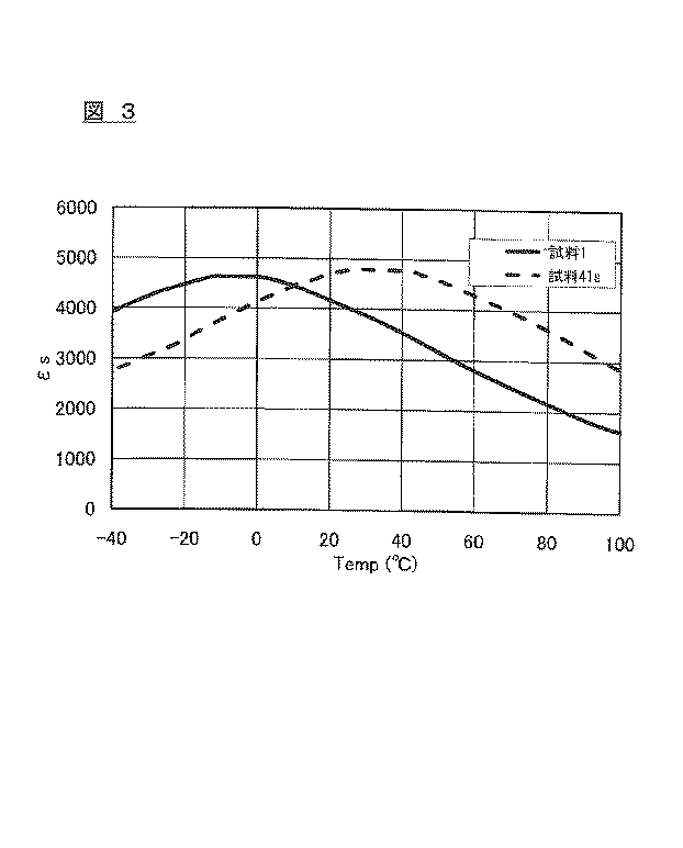
コンデンサ試料の雰囲気温度を−40〜100℃に変化させた際の温度に対する比誘電率の関係をグラフ化し、変曲点をキュリー温度(Cp)とした。なお、比誘電率は前記方法により測定した。キュリー温度が室温よりも高いと、コンデンサを室温で用いた場合、熱暴走するおそれがある。したがって、本実施例では20℃以下を好ましい範囲とした。また、試料1と試料41sについては、−40〜100℃の範囲における比誘電率の変化を表すグラフを図3に示す。
(Curie temperature (Cp))
The relationship between the relative dielectric constant and the temperature when the ambient temperature of the capacitor sample was changed from −40 to 100 ° C. was graphed, and the inflection point was defined as the Curie temperature (Cp). The relative dielectric constant was measured by the above method. If the Curie temperature is higher than room temperature, there is a risk of thermal runaway when the capacitor is used at room temperature. Therefore, in this example, 20 ° C. or less was set as a preferable range. Moreover, about the
(温度特性(TC))
コンデンサ試料に対し、−25℃と85℃において、デジタルLCRメータ(YHP社製4284A)にて、周波数1kHz、入力信号レベル(測定電圧)1Vrmsの条件で静電容量を測定し、基準温度20℃における静電容量に対する−25℃および85℃での静電容量の変化率(単位は%)を算出した。本実施例ではΔC/C20は、+20%〜−55%が好ましい範囲とし、−25℃と85℃の両方でこの範囲を満たす場合は「○」、少なくとも一方が外れる場合には「×」とした。
(Temperature characteristics (TC))
The capacitance of the capacitor sample was measured at −25 ° C. and 85 ° C. using a digital LCR meter (YHP 4284A) under the conditions of a frequency of 1 kHz and an input signal level (measurement voltage) of 1 Vrms, and a reference temperature of 20 ° C. The change rate (unit:%) of the capacitance at −25 ° C. and 85 ° C. with respect to the capacitance was calculated. In this example, ΔC / C20 is preferably in a range of + 20% to −55%, and “◯” when the range is satisfied at both −25 ° C. and 85 ° C., and “X” when at least one of them is off. did.
(焼結性)
得られた焼結体について、焼成後の焼結体の寸法および重量から、焼結体密度を算出し、その焼結体密度が5.2g/cm3以上のものを○、5.2g/cm3未満の物を×とした。ここで、基準を5.2g/cm3未満としたのは、5.2g/cm3未満だと素地の強度が著しく低下してしまうためである。
(Sinterability)
With respect to the obtained sintered body, the sintered body density was calculated from the size and weight of the sintered body after firing, and the sintered body density was 5.2 g / cm 3 or more. The thing below cm 3 was made into x. Here, the reason why the reference is less than 5.2 g / cm 3 is that the strength of the substrate is remarkably lowered when it is less than 5.2 g / cm 3 .
試料2〜61
試料2〜61(表1、2)に示す組成となるように秤量した以外は、試料1と同様にして各コンデンサ試料を得た後、比誘電率、誘電損失、交流破壊電圧、キュリー温度、温度特性および焼結性を評価した。結果を表3または4に示す。
Samples 2-61
Except for weighing to the compositions shown in
試料1〜12より、組成式中のαが0.95〜1.02の場合は(試料1、3〜11)、αが1.020を超える場合(試料2)に比べ、焼結性が良好であることが確認できた。また、組成式中のαが0.95〜1.02の場合は(試料1、3〜11)、αが0.95未満の場合(試料12)に比べ、比誘電率が高くなり、誘電損失およびキュリー温度が低くなることが確認できた。
From
試料1、13〜21より、組成式中のuが0.20〜0.27の場合(試料1、14〜20)には、uが0.27を超える場合(試料13)に比べ、比誘電率が高くなり、誘電損失が低くなることが確認できた。また、組成式中のuが0.20≦u≦0.27の場合(試料1、14〜20)には、uが0.20未満の場合(試料21)に比べ、温度特性が良好になることが確認できた。
From
試料1、22〜26より、組成式中のvが0.018〜0.049の場合は(試料1、23〜25)、vが0.048を超える場合(試料22)に比べ、比誘電率が高くなり、焼結性が良好であることが確認できた。また、組成式中のvが0.018〜0.049の場合は(試料1、23〜25)、vが0.018未満の場合(試料26)に比べ、交流破壊電圧が高くなり、温度特性が良好になることが確認できた。
From
試料1、27〜33より、組成式中のwが0.004〜0.018の場合は(試料1、28〜32)、wが0.018を超える場合(試料27)に比べ、温度特性が良好になることが確認できた。また、組成式中のwが0.004〜0.018の場合は(試料1、28〜32)、wが0.004未満の場合(試料33)に比べ、誘電損失が低くなることが確認できた。
From
試料1、34〜41より、組成式中のxが0.118〜0.149の場合は(試料35〜40)、xが0.149を超える場合(試料34)に比べ、交流破壊電圧が高くなり、温度特性が良好になることが確認できた。また、組成式中のxが0.118〜0.149の場合は(試料35〜40)、xが0.118未満の場合(試料41)に比べ、交流破壊電圧が高くなり、温度特性が良好になり、誘電損失が低くなることが確認できた。
From
試料1、42〜48より、酸化ニッケルの含有量が主成分100重量部に対して0.03〜0.4重量部の場合は(試料1、43〜47)、酸化ニッケルの含有量0.4重量部を超える場合(試料42)に比べ、比誘電率および交流破壊電圧が高くなり、焼結性が良好になることが確認できた。また、酸化ニッケルの含有量が主成分100重量部に対して0.03〜0.4重量部の場合は(試料1、43〜47)、酸化ニッケルの含有量が0.03重量部未満の場合(試料48)に比べ、比誘電率および交流破壊電圧が高くなることが確認できた。
From the
試料1、49〜55より、酸化セリウムの含有量が主成分100重量部に対して0.03〜0.4重量部の場合は(試料50〜54)、酸化セリウムの含有量が0.4重量部を超える場合(試料49)に比べ、比誘電率が高くなり、誘電損失が低くなり、温度特性が良好になることが確認できた。また、酸化セリウムの含有量が主成分100重量部に対して0.03〜0.4重量部の場合は(試料50〜54)、酸化セリウムの含有量が0.03重量部未満の場合(試料55)に比べ、交流破壊電圧が高くなり、温度特性が良好になることが確認できた。
From
試料1、56〜60より、酸化マンガンの含有量が主成分100重量に対して0.03〜0.4重量部の場合は(試料1、57〜59)、酸化マンガンの含有量が0.4重量部を超える場合(試料56)に比べ、比誘電率および交流破壊電圧が高くなり誘電損失が低くなることが確認できた。また、酸化マンガンの含有量が主成分100重量に対して0.03〜0.4重量部の場合は(試料1、57〜59)、酸化マンガンの含有量が0.03重量部未満の場合(試料60)に比べ比誘電率が高くなり焼結性が良好になることが確認できた。
From
なお、主成分の組成はuが0.20〜0.27、vが0.018〜0.049、wが0.004〜0.018、xが0.118〜0.149、αが0.95〜1.02を満たしていても、副成分を含まない場合は(試料61)、比誘電率および交流破壊電圧が低下し、誘電損失が上昇し、焼結性が悪くなることが確認できた。 The composition of the main components is u = 0.20 to 0.27, v is 0.018 to 0.049, w is 0.004 to 0.018, x is 0.118 to 0.149, and α is 0. Even if it satisfies .95 to 1.02 but does not contain subcomponents (Sample 61), it is confirmed that the dielectric constant and AC breakdown voltage are lowered, the dielectric loss is increased, and the sinterability is deteriorated. did it.
さらに、図3(A)より試料1はキュリー温度が−10℃であり、−10℃を超えると温度の上昇とともに比誘電率が低下することが確認できた。このように、キュリー温度が−10℃と低いことで、室温(20℃)付近では、温度の上昇とともに比誘電率が低下する。これにより、交流電場印加により試料が発熱しても比誘電率が低下していき発熱が抑えられるため、発熱が更なる発熱を招くという正のフィードバックを回避することとなり、熱暴走を防ぐことができる。
Furthermore, from FIG. 3A, it was confirmed that
一方、図3(B)より試料41sはキュリー温度が35℃であり、35℃以下では温度の上昇とともに比誘電率が上昇し、35℃以上では温度の上昇とともに比誘電率が低下することが確認できた。このように、キュリー温度が35℃と高いと、室温20℃付近では、温度の上昇とともにキュリー温度までは比誘電率が上昇する。これにより、交流電場印加により試料が発熱しても比誘電率が低下しないため、発熱が更なる発熱を招くという正のフィードバック状態となり、熱暴走する可能性がある。 On the other hand, as shown in FIG. 3B, the sample 41s has a Curie temperature of 35 ° C., and the dielectric constant increases with increasing temperature below 35 ° C., and the relative dielectric constant decreases with increasing temperature above 35 ° C. It could be confirmed. Thus, when the Curie temperature is as high as 35 ° C., the relative dielectric constant increases up to the Curie temperature as the temperature rises near the room temperature of 20 ° C. As a result, even if the sample generates heat due to application of an alternating electric field, the relative permittivity does not decrease, so that a positive feedback state in which heat generation causes further heat generation may occur, and thermal runaway may occur.
2… 単板型セラミックコンデンサ
4… 保護樹脂
6,8… リード端子
10… 誘電体層
12,14… 端子電極
22… 貫通型コンデンサ
210… 誘電体層
212a、212b… 個別電極
214… 共通電極
216a、216b… 貫通孔
2 ... Single plate type
Claims (2)
前記組成式中のuが0.20〜0.27であり、
前記組成式中のvが0.018〜0.049であり、
前記組成式中のwが0.004〜0.018であり、
前記組成式中のxが0.118〜0.149であり、
前記組成式中のαが0.95〜1.02であり、
前記酸化ニッケルを前記主成分100重量部に対して0.03〜0.4重量部含有し、
前記酸化セリウムを前記主成分100重量部に対して0.03〜0.4重量部含有し、
前記酸化マンガンを前記主成分100重量部に対して0.03〜0.4重量部含有する誘電体磁器組成物。 A main component (Ba 1-u-v- w, Ca u, Mg v, Sr w) expressed α (Ti 1-x, Zr x) by the composition formula of O 3, nickel oxide, and cerium oxide, A dielectric porcelain composition comprising manganese,
U in the composition formula is 0.20 to 0.27,
V in the composition formula is 0.018 to 0.049,
W in the composition formula is 0.004 to 0.018,
X in the composition formula is 0.118 to 0.149,
Α in the composition formula is 0.95 to 1.02,
Containing 0.03 to 0.4 parts by weight of the nickel oxide with respect to 100 parts by weight of the main component,
Containing 0.03 to 0.4 parts by weight of the cerium oxide with respect to 100 parts by weight of the main component,
A dielectric ceramic composition comprising 0.03 to 0.4 parts by weight of the manganese oxide with respect to 100 parts by weight of the main component.
The electronic component which has a dielectric material layer comprised with the dielectric material ceramic composition of Claim 1.
Priority Applications (3)
| Application Number | Priority Date | Filing Date | Title |
|---|---|---|---|
| JP2010057662A JP5418323B2 (en) | 2010-03-15 | 2010-03-15 | Dielectric porcelain composition and electronic component |
| KR1020110022402A KR101178952B1 (en) | 2010-03-15 | 2011-03-14 | Dielectric ceramic composition and electronic component |
| CN2011100617313A CN102190494B (en) | 2010-03-15 | 2011-03-15 | Dielectric ceramic composition and electronic component |
Applications Claiming Priority (1)
| Application Number | Priority Date | Filing Date | Title |
|---|---|---|---|
| JP2010057662A JP5418323B2 (en) | 2010-03-15 | 2010-03-15 | Dielectric porcelain composition and electronic component |
Publications (2)
| Publication Number | Publication Date |
|---|---|
| JP2011190145A JP2011190145A (en) | 2011-09-29 |
| JP5418323B2 true JP5418323B2 (en) | 2014-02-19 |
Family
ID=44599464
Family Applications (1)
| Application Number | Title | Priority Date | Filing Date |
|---|---|---|---|
| JP2010057662A Active JP5418323B2 (en) | 2010-03-15 | 2010-03-15 | Dielectric porcelain composition and electronic component |
Country Status (3)
| Country | Link |
|---|---|
| JP (1) | JP5418323B2 (en) |
| KR (1) | KR101178952B1 (en) |
| CN (1) | CN102190494B (en) |
Families Citing this family (6)
| Publication number | Priority date | Publication date | Assignee | Title |
|---|---|---|---|---|
| TWI581472B (en) * | 2012-11-02 | 2017-05-01 | 佳能股份有限公司 | Piezoelectric material, piezoelectric element, and electronic device |
| CN104821224A (en) * | 2015-05-18 | 2015-08-05 | 中国科学技术大学 | Inductance based on piezoceramic ceramic material and application thereof |
| JP6696267B2 (en) * | 2016-03-30 | 2020-05-20 | Tdk株式会社 | Dielectric ceramic composition and multilayer ceramic capacitor |
| CN106986634A (en) * | 2017-04-28 | 2017-07-28 | 信阳师范学院 | A kind of calcium barium zirconate titanate base piezoceramics and preparation method thereof |
| CN108249917B (en) * | 2018-01-05 | 2020-04-24 | 杭州电子科技大学 | Microwave dielectric ceramic with medium dielectric constant and ultralow dielectric loss, preparation method and application thereof |
| CN113956038A (en) * | 2021-12-01 | 2022-01-21 | 中国科学院新疆理化技术研究所 | Cerium-doped perovskite type high-temperature thermal sensitive ceramic resistor material and preparation method thereof |
Family Cites Families (7)
| Publication number | Priority date | Publication date | Assignee | Title |
|---|---|---|---|---|
| JPS60101803A (en) * | 1983-11-08 | 1985-06-05 | 松下電器産業株式会社 | Composition for high dielectric constant porcelain material |
| JP2518184B2 (en) * | 1989-02-06 | 1996-07-24 | 株式会社村田製作所 | Monolithic ceramic capacitors |
| JP2824083B2 (en) * | 1989-07-31 | 1998-11-11 | ティーディーケイ株式会社 | Dielectric porcelain composition |
| JP3269902B2 (en) * | 1993-12-29 | 2002-04-02 | 太陽誘電株式会社 | Porcelain capacitor and method of manufacturing the same |
| JP3279856B2 (en) * | 1995-02-14 | 2002-04-30 | ティーディーケイ株式会社 | Dielectric porcelain composition |
| JP3606079B2 (en) | 1998-12-25 | 2005-01-05 | 株式会社村田製作所 | Nonlinear dielectric porcelain, capacitor for pulse generation, high pressure steam discharge lamp circuit and high pressure steam discharge lamp |
| JP3470703B2 (en) | 2000-04-07 | 2003-11-25 | 株式会社村田製作所 | Non-reducing dielectric ceramic, multilayer ceramic capacitor using the same, and method for producing non-reducing dielectric ceramic |
-
2010
- 2010-03-15 JP JP2010057662A patent/JP5418323B2/en active Active
-
2011
- 2011-03-14 KR KR1020110022402A patent/KR101178952B1/en active Active
- 2011-03-15 CN CN2011100617313A patent/CN102190494B/en active Active
Also Published As
| Publication number | Publication date |
|---|---|
| KR101178952B1 (en) | 2012-08-31 |
| KR20110103878A (en) | 2011-09-21 |
| CN102190494A (en) | 2011-09-21 |
| CN102190494B (en) | 2013-09-11 |
| JP2011190145A (en) | 2011-09-29 |
Similar Documents
| Publication | Publication Date | Title |
|---|---|---|
| JP5664228B2 (en) | Dielectric porcelain composition and electronic component | |
| JP5272754B2 (en) | Dielectric porcelain composition and electronic component | |
| JP5910317B2 (en) | Dielectric porcelain composition and electronic component | |
| JP5278682B2 (en) | Dielectric porcelain composition and electronic component | |
| JP5418323B2 (en) | Dielectric porcelain composition and electronic component | |
| JP6696267B2 (en) | Dielectric ceramic composition and multilayer ceramic capacitor | |
| JP2008174413A (en) | Dielectric porcelain composition and electronic component | |
| JP5012932B2 (en) | Dielectric porcelain composition and electronic component | |
| JP6413861B2 (en) | Dielectric porcelain composition and electronic component | |
| JP2007063040A (en) | Method for producing dielectric porcelain composition, and electronic component | |
| JP6376001B2 (en) | Dielectric composition | |
| TWI476170B (en) | Dielectric ceramic compositions and electronic components | |
| JP4710574B2 (en) | Dielectric porcelain composition and electronic component | |
| TWI412504B (en) | A dielectric ceramic composition, a method for preparing a dielectric ceramic composition, and an electronic component | |
| JP2007161538A (en) | Reduction resistant dielectric ceramic composition, electronic component and laminated ceramic capacitor | |
| JP6020068B2 (en) | Dielectric porcelain composition and electronic component | |
| KR101429034B1 (en) | Dielectric ceramic composition and electronic component | |
| JP2005132698A (en) | Electronic component, dielectric porcelain composition, and its production method | |
| TWI443079B (en) | Dielectric ceramic compositions and electronic components | |
| JP2007153710A (en) | Dielectric porcelain composition and electronic component | |
| JP2007269542A (en) | Dielectric porcelain composition and electronic component | |
| JP2007091551A (en) | Dielectric porcelain composition | |
| JP2011198947A (en) | Ceramic electronic component, and method of manufacturing ceramic electronic component |
Legal Events
| Date | Code | Title | Description |
|---|---|---|---|
| A621 | Written request for application examination |
Free format text: JAPANESE INTERMEDIATE CODE: A621 Effective date: 20121114 |
|
| A977 | Report on retrieval |
Free format text: JAPANESE INTERMEDIATE CODE: A971007 Effective date: 20130925 |
|
| RD05 | Notification of revocation of power of attorney |
Free format text: JAPANESE INTERMEDIATE CODE: A7425 Effective date: 20131004 |
|
| TRDD | Decision of grant or rejection written | ||
| A01 | Written decision to grant a patent or to grant a registration (utility model) |
Free format text: JAPANESE INTERMEDIATE CODE: A01 Effective date: 20131022 |
|
| A61 | First payment of annual fees (during grant procedure) |
Free format text: JAPANESE INTERMEDIATE CODE: A61 Effective date: 20131104 |
|
| R150 | Certificate of patent or registration of utility model |
Ref document number: 5418323 Country of ref document: JP Free format text: JAPANESE INTERMEDIATE CODE: R150 |
|
| R250 | Receipt of annual fees |
Free format text: JAPANESE INTERMEDIATE CODE: R250 |