JP5474002B2 - マルチチップ・ウェハレベル・パッケージを形成する方法 - Google Patents
マルチチップ・ウェハレベル・パッケージを形成する方法 Download PDFInfo
- Publication number
- JP5474002B2 JP5474002B2 JP2011160519A JP2011160519A JP5474002B2 JP 5474002 B2 JP5474002 B2 JP 5474002B2 JP 2011160519 A JP2011160519 A JP 2011160519A JP 2011160519 A JP2011160519 A JP 2011160519A JP 5474002 B2 JP5474002 B2 JP 5474002B2
- Authority
- JP
- Japan
- Prior art keywords
- chip
- chips
- wafer
- forming
- area
- Prior art date
- Legal status (The legal status is an assumption and is not a legal conclusion. Google has not performed a legal analysis and makes no representation as to the accuracy of the status listed.)
- Expired - Fee Related
Links
Images




Classifications
-
- H—ELECTRICITY
- H10—SEMICONDUCTOR DEVICES; ELECTRIC SOLID-STATE DEVICES NOT OTHERWISE PROVIDED FOR
- H10P—GENERIC PROCESSES OR APPARATUS FOR THE MANUFACTURE OR TREATMENT OF DEVICES COVERED BY CLASS H10
- H10P95/00—Generic processes or apparatus for manufacture or treatments not covered by the other groups of this subclass
-
- H—ELECTRICITY
- H10—SEMICONDUCTOR DEVICES; ELECTRIC SOLID-STATE DEVICES NOT OTHERWISE PROVIDED FOR
- H10W—GENERIC PACKAGES, INTERCONNECTIONS, CONNECTORS OR OTHER CONSTRUCTIONAL DETAILS OF DEVICES COVERED BY CLASS H10
- H10W70/00—Package substrates; Interposers; Redistribution layers [RDL]
- H10W70/60—Insulating or insulated package substrates; Interposers; Redistribution layers
- H10W70/611—Insulating or insulated package substrates; Interposers; Redistribution layers for connecting multiple chips together
- H10W70/614—Insulating or insulated package substrates; Interposers; Redistribution layers for connecting multiple chips together the multiple chips being integrally enclosed
-
- H—ELECTRICITY
- H10—SEMICONDUCTOR DEVICES; ELECTRIC SOLID-STATE DEVICES NOT OTHERWISE PROVIDED FOR
- H10P—GENERIC PROCESSES OR APPARATUS FOR THE MANUFACTURE OR TREATMENT OF DEVICES COVERED BY CLASS H10
- H10P54/00—Cutting or separating of wafers, substrates or parts of devices
-
- H—ELECTRICITY
- H10—SEMICONDUCTOR DEVICES; ELECTRIC SOLID-STATE DEVICES NOT OTHERWISE PROVIDED FOR
- H10W—GENERIC PACKAGES, INTERCONNECTIONS, CONNECTORS OR OTHER CONSTRUCTIONAL DETAILS OF DEVICES COVERED BY CLASS H10
- H10W70/00—Package substrates; Interposers; Redistribution layers [RDL]
- H10W70/60—Insulating or insulated package substrates; Interposers; Redistribution layers
-
- H—ELECTRICITY
- H10—SEMICONDUCTOR DEVICES; ELECTRIC SOLID-STATE DEVICES NOT OTHERWISE PROVIDED FOR
- H10W—GENERIC PACKAGES, INTERCONNECTIONS, CONNECTORS OR OTHER CONSTRUCTIONAL DETAILS OF DEVICES COVERED BY CLASS H10
- H10W70/00—Package substrates; Interposers; Redistribution layers [RDL]
- H10W70/60—Insulating or insulated package substrates; Interposers; Redistribution layers
- H10W70/611—Insulating or insulated package substrates; Interposers; Redistribution layers for connecting multiple chips together
-
- H—ELECTRICITY
- H10—SEMICONDUCTOR DEVICES; ELECTRIC SOLID-STATE DEVICES NOT OTHERWISE PROVIDED FOR
- H10W—GENERIC PACKAGES, INTERCONNECTIONS, CONNECTORS OR OTHER CONSTRUCTIONAL DETAILS OF DEVICES COVERED BY CLASS H10
- H10W70/00—Package substrates; Interposers; Redistribution layers [RDL]
- H10W70/60—Insulating or insulated package substrates; Interposers; Redistribution layers
- H10W70/67—Insulating or insulated package substrates; Interposers; Redistribution layers characterised by their insulating layers or insulating parts
- H10W70/69—Insulating materials thereof
- H10W70/698—Semiconductor materials that are electrically insulating, e.g. undoped silicon
-
- H—ELECTRICITY
- H10—SEMICONDUCTOR DEVICES; ELECTRIC SOLID-STATE DEVICES NOT OTHERWISE PROVIDED FOR
- H10W—GENERIC PACKAGES, INTERCONNECTIONS, CONNECTORS OR OTHER CONSTRUCTIONAL DETAILS OF DEVICES COVERED BY CLASS H10
- H10W72/00—Interconnections or connectors in packages
-
- H—ELECTRICITY
- H10—SEMICONDUCTOR DEVICES; ELECTRIC SOLID-STATE DEVICES NOT OTHERWISE PROVIDED FOR
- H10W—GENERIC PACKAGES, INTERCONNECTIONS, CONNECTORS OR OTHER CONSTRUCTIONAL DETAILS OF DEVICES COVERED BY CLASS H10
- H10W72/00—Interconnections or connectors in packages
- H10W72/071—Connecting or disconnecting
-
- H—ELECTRICITY
- H10—SEMICONDUCTOR DEVICES; ELECTRIC SOLID-STATE DEVICES NOT OTHERWISE PROVIDED FOR
- H10W—GENERIC PACKAGES, INTERCONNECTIONS, CONNECTORS OR OTHER CONSTRUCTIONAL DETAILS OF DEVICES COVERED BY CLASS H10
- H10W90/00—Package configurations
- H10W90/401—Package configurations characterised by multiple insulating or insulated package substrates, interposers or RDLs
-
- H—ELECTRICITY
- H10—SEMICONDUCTOR DEVICES; ELECTRIC SOLID-STATE DEVICES NOT OTHERWISE PROVIDED FOR
- H10P—GENERIC PROCESSES OR APPARATUS FOR THE MANUFACTURE OR TREATMENT OF DEVICES COVERED BY CLASS H10
- H10P72/00—Handling or holding of wafers, substrates or devices during manufacture or treatment thereof
- H10P72/70—Handling or holding of wafers, substrates or devices during manufacture or treatment thereof for supporting or gripping
- H10P72/74—Handling or holding of wafers, substrates or devices during manufacture or treatment thereof for supporting or gripping using temporarily an auxiliary support
- H10P72/7412—Handling or holding of wafers, substrates or devices during manufacture or treatment thereof for supporting or gripping using temporarily an auxiliary support the auxiliary support including means facilitating the separation of a device or wafer from the auxiliary support
- H10P72/7414—Handling or holding of wafers, substrates or devices during manufacture or treatment thereof for supporting or gripping using temporarily an auxiliary support the auxiliary support including means facilitating the separation of a device or wafer from the auxiliary support the auxiliary support including means facilitating the selective separation of some of a plurality of devices from the auxiliary support
-
- H—ELECTRICITY
- H10—SEMICONDUCTOR DEVICES; ELECTRIC SOLID-STATE DEVICES NOT OTHERWISE PROVIDED FOR
- H10P—GENERIC PROCESSES OR APPARATUS FOR THE MANUFACTURE OR TREATMENT OF DEVICES COVERED BY CLASS H10
- H10P72/00—Handling or holding of wafers, substrates or devices during manufacture or treatment thereof
- H10P72/70—Handling or holding of wafers, substrates or devices during manufacture or treatment thereof for supporting or gripping
- H10P72/74—Handling or holding of wafers, substrates or devices during manufacture or treatment thereof for supporting or gripping using temporarily an auxiliary support
- H10P72/7424—Handling or holding of wafers, substrates or devices during manufacture or treatment thereof for supporting or gripping using temporarily an auxiliary support used as a support during the manufacture of self-supporting substrates
Landscapes
- Semiconductor Integrated Circuits (AREA)
- Dicing (AREA)
- Wire Bonding (AREA)
- Crystals, And After-Treatments Of Crystals (AREA)
Description
Claims (8)
- マルチチップ・ウェハレベル・パッケージを形成する方法であって、
複数のチップ基板上に複数の異種チップを形成するステップであって、前記複数のチップ基板の各々はただ1種のチップを形成するために用いられるステップと、
前記複数のチップ基板から前記複数の異種チップを取り外すステップと、
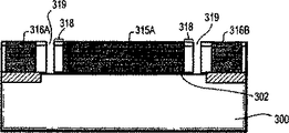
キャリア基板中にポケットを形成するステップであって、各々のポケットは前記異種チップの1つを保持するステップと、
前記複数のチップを前記キャリア基板中のそれらの対応するポケット内に、前記複数のチップの最表面が前記キャリア基板の最表面と実質的に同一平面になるように取り付けるステップとを含み、
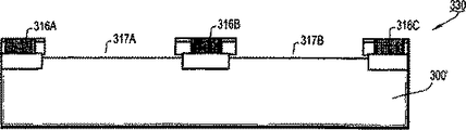
複数のチップ基板上に複数のチップを形成する前記ステップは、ウェハを各チップ基板中の浅いトレンチ分離(STI)領域に、前記STI領域に隣接しかつ前記ウェハとチップ基板との間に空隙が形成されるように接合するステップを含み、前記STI領域上方の前記ウェハ中のエリアがチップ間エリアを画定し、前記空隙上方の前記ウェハ中のエリアがチップ・エリアを画定し、
前記チップ基板の前記チップ間エリア中にディスクリート・デバイスを形成するステップをさらに含み、
前記複数のチップとは、
前記複数の異種のチップのうちの複数の互いに異なる種類のチップ、又は、複数の互いに異なる種類のチップと複数の同じ種類のチップの両方である、方法。 - マルチチップ・ウェハレベル・パッケージを形成する方法であって、
複数のチップ基板上に複数の異種チップを形成するステップであって、前記複数のチップ基板の各々はただ1種のチップを形成するために用いられるステップと、
前記複数のチップ基板から前記複数の異種チップを取り外すステップと、
キャリア基板中にポケットを形成するステップであって、各々のポケットは前記異種チップの1つを保持するステップと、
前記複数のチップを前記キャリア基板中のそれらの対応するポケット内に、前記複数のチップの最表面が前記キャリア基板の最表面と実質的に同一平面になるように取り付けるステップとを含み、
複数のチップ基板上に複数のチップを形成する前記ステップは、ウェハを各チップ基板中の浅いトレンチ分離(STI)領域に、前記STI領域に隣接しかつ前記ウェハとチップ基板との間に空隙が形成されるように接合するステップを含み、前記STI領域上方の前記ウェハ中のエリアがチップ間エリアを画定し、前記空隙上方の前記ウェハ中のエリアがチップ・エリアを画定し、
前記チップ基板の前記チップ間エリアに形成されるデバイスは、前記空隙情報のウェハ中に形成されるデバイスの試験及び監視のためにのみ用いられ、
前記複数のチップとは、前記複数の異種のチップのうちの複数の互いに異なる種類のチップ、又は、複数の互いに異なる種類のチップと複数の同じ種類のチップの両方のいずれかである、方法。 - 前記ウェハを前記STI領域に接合するステップの前に、
前記チップ基板上に誘電体層をパターン形成するステップと、
オフチップ・エリアを画定するために前記パターン形成された誘電体層をエッチングするステップと、
前記オフチップ・エリア中にSTI領域を形成するステップと、
前記オフチップ・エリアの間の前記誘電体層を除去するステップとを含む、
請求項1または2に記載の方法。 - 前記ウェハを薄化するステップと、
前記薄化されたウェハ中にデバイスを形成するステップと、
前記薄化されたウェハ上に後工程(BEOL)相互接続部を形成するステップと、
前記チップ・エリア中に最終仕上げデバイスおよび相互接続部を形成して、前記複数のチップの形成を完了するステップとをさらに含む、請求項1または2に記載の方法。 - 前記複数のチップを前記複数のチップ基板から取り外す前記ステップは、
前記薄化されたウェハの最表面をパッシベーション層でコーティングするステップと
前記薄化されたウェハの前記チップ・エリアを通り前記空隙までチャネルをダイシングし、それによって前記複数のチップを前記複数のチップ基板から取り外すステップとを含む、請求項4に記載の方法。 - マルチチップ・ウェハレベル・パッケージを形成する方法であって、
チップ基板中に浅いトレンチ分離(STI)領域を形成するステップと、
ウェハを前記チップ基板中のSTI領域に、前記STI領域に隣接しかつ前記ウェハと前記チップ基板との間に空隙が形成されるように接合するステップであって、前記STI領域上方の前記ウェハ中のエリアはチップ間エリアを画定し、前記空隙上方の前記ウェハ中のエリアはチップ・エリアを画定するステップと、
前記ウェハを薄化するステップと、
前記薄化されたウェハ中にデバイスを形成するステップと、
前記薄化されたウェハ上に後工程(BEOL)相互接続部を形成するステップと、
前記チップ・エリア中に最終仕上げデバイスおよび相互接続部を形成し、複数のチップの前記形成を完了するステップとを含み、
前記チップ基板の前記チップ間エリア中にディスクリート・デバイスを形成するステップをさらに含む、方法。 - 前記薄化されたウェハの最表面をパッシベーション層でコーティングするステップと
前記薄化されたウェハの前記チップ・エリアを通り前記空隙までチャネルをダイシングし、それによって前記複数のチップを前記複数のチップ基板から取り外すステップとをさらに含む、請求項6に記載の方法。 - 前記薄化されたウェハの所定部分が取り外され、それによって前記薄化されたウェハ内にポケットを形成するように、前記薄化されたウェハの前記チップ・エリア中にチャネルをダイシングするステップをさらに含む、請求項7に記載の方法。
Applications Claiming Priority (2)
| Application Number | Priority Date | Filing Date | Title |
|---|---|---|---|
| US10/994,494 | 2004-11-20 | ||
| US10/994,494 US7405108B2 (en) | 2004-11-20 | 2004-11-20 | Methods for forming co-planar wafer-scale chip packages |
Related Parent Applications (1)
| Application Number | Title | Priority Date | Filing Date |
|---|---|---|---|
| JP2007541952A Division JP5459959B2 (ja) | 2004-11-20 | 2005-11-16 | マルチチップ・ウェハレベル・パッケージを形成する方法 |
Publications (2)
| Publication Number | Publication Date |
|---|---|
| JP2011249830A JP2011249830A (ja) | 2011-12-08 |
| JP5474002B2 true JP5474002B2 (ja) | 2014-04-16 |
Family
ID=35735294
Family Applications (2)
| Application Number | Title | Priority Date | Filing Date |
|---|---|---|---|
| JP2007541952A Expired - Fee Related JP5459959B2 (ja) | 2004-11-20 | 2005-11-16 | マルチチップ・ウェハレベル・パッケージを形成する方法 |
| JP2011160519A Expired - Fee Related JP5474002B2 (ja) | 2004-11-20 | 2011-07-22 | マルチチップ・ウェハレベル・パッケージを形成する方法 |
Family Applications Before (1)
| Application Number | Title | Priority Date | Filing Date |
|---|---|---|---|
| JP2007541952A Expired - Fee Related JP5459959B2 (ja) | 2004-11-20 | 2005-11-16 | マルチチップ・ウェハレベル・パッケージを形成する方法 |
Country Status (9)
| Country | Link |
|---|---|
| US (2) | US7405108B2 (ja) |
| EP (1) | EP1817793B1 (ja) |
| JP (2) | JP5459959B2 (ja) |
| KR (1) | KR100992015B1 (ja) |
| CN (1) | CN100437952C (ja) |
| AT (1) | ATE477588T1 (ja) |
| DE (1) | DE602005022919D1 (ja) |
| TW (1) | TWI362706B (ja) |
| WO (1) | WO2006053879A1 (ja) |
Families Citing this family (27)
| Publication number | Priority date | Publication date | Assignee | Title |
|---|---|---|---|---|
| US7405108B2 (en) * | 2004-11-20 | 2008-07-29 | International Business Machines Corporation | Methods for forming co-planar wafer-scale chip packages |
| US7442579B2 (en) * | 2004-11-22 | 2008-10-28 | International Business Machines Corporation | Methods to achieve precision alignment for wafer scale packages |
| DE102005039479B3 (de) * | 2005-08-18 | 2007-03-29 | Infineon Technologies Ag | Halbleiterbauteil mit gedünntem Halbleiterchip und Verfahren zur Herstellung des gedünnten Halbleiterbauteils |
| US7658901B2 (en) * | 2005-10-14 | 2010-02-09 | The Trustees Of Princeton University | Thermally exfoliated graphite oxide |
| JP4559993B2 (ja) * | 2006-03-29 | 2010-10-13 | 株式会社東芝 | 半導体装置の製造方法 |
| KR100829392B1 (ko) * | 2006-08-24 | 2008-05-13 | 동부일렉트로닉스 주식회사 | SoC 및 그 제조 방법 |
| TW200941661A (en) * | 2008-03-19 | 2009-10-01 | Integrated Circuit Solution Inc | Shape of window formed in a substrate for window ball grid array package |
| JP4828559B2 (ja) * | 2008-03-24 | 2011-11-30 | 新光電気工業株式会社 | 配線基板の製造方法及び電子装置の製造方法 |
| US8772087B2 (en) * | 2009-10-22 | 2014-07-08 | Infineon Technologies Ag | Method and apparatus for semiconductor device fabrication using a reconstituted wafer |
| US8322022B1 (en) | 2010-06-28 | 2012-12-04 | Western Digital (Fremont), Llc | Method for providing an energy assisted magnetic recording head in a wafer packaging configuration |
| CN102386088B (zh) * | 2010-09-03 | 2014-06-25 | 中芯国际集成电路制造(上海)有限公司 | 用于去除半导体器件结构上的光致抗蚀剂层的方法 |
| CN102769002B (zh) * | 2011-04-30 | 2016-09-14 | 中国科学院微电子研究所 | 半导体器件及其形成方法、封装结构 |
| JP6063641B2 (ja) * | 2012-05-16 | 2017-01-18 | 株式会社ディスコ | ウエーハ保護部材 |
| WO2015043495A1 (zh) * | 2013-09-30 | 2015-04-02 | 南通富士通微电子股份有限公司 | 晶圆封装结构和封装方法 |
| US9123546B2 (en) * | 2013-11-14 | 2015-09-01 | Taiwan Semiconductor Manufacturing Company Limited | Multi-layer semiconductor device structures with different channel materials |
| US9350339B2 (en) | 2014-07-18 | 2016-05-24 | Qualcomm Incorporated | Systems and methods for clock distribution in a die-to-die interface |
| CN109196405B (zh) | 2016-05-27 | 2021-09-10 | 浜松光子学株式会社 | 法布里-帕罗干涉滤光器的制造方法 |
| JP6341959B2 (ja) | 2016-05-27 | 2018-06-13 | 浜松ホトニクス株式会社 | ファブリペロー干渉フィルタの製造方法 |
| CN118091929A (zh) | 2016-08-24 | 2024-05-28 | 浜松光子学株式会社 | 法布里-珀罗干涉滤光器 |
| US10916507B2 (en) | 2018-12-04 | 2021-02-09 | International Business Machines Corporation | Multiple chip carrier for bridge assembly |
| GB2582384B (en) * | 2019-03-22 | 2023-10-18 | Cirrus Logic Int Semiconductor Ltd | Semiconductor structures |
| US11456247B2 (en) * | 2019-06-13 | 2022-09-27 | Nanya Technology Corporation | Semiconductor device and fabrication method for the same |
| CN110690868B (zh) * | 2019-09-27 | 2021-02-19 | 无锡市好达电子股份有限公司 | 一种滤波器的新型晶圆级封装方法 |
| CN111128716B (zh) * | 2019-11-15 | 2023-10-17 | 西安电子科技大学 | 一种大面积图形自对准的异质集成方法 |
| KR102766434B1 (ko) | 2020-03-26 | 2025-02-12 | 삼성전자주식회사 | 반도체 스택 및 그 제조 방법 |
| US11545404B2 (en) * | 2020-05-06 | 2023-01-03 | Qualcomm Incorporated | III-V compound semiconductor dies with stress-treated inactive surfaces to avoid packaging-induced fractures, and related methods |
| TWI790003B (zh) * | 2021-11-18 | 2023-01-11 | 佳邦科技股份有限公司 | 過電壓保護元件 |
Family Cites Families (21)
| Publication number | Priority date | Publication date | Assignee | Title |
|---|---|---|---|---|
| JPS6281745A (ja) * | 1985-10-05 | 1987-04-15 | Fujitsu Ltd | ウエハ−規模のlsi半導体装置とその製造方法 |
| US4866501A (en) * | 1985-12-16 | 1989-09-12 | American Telephone And Telegraph Company At&T Bell Laboratories | Wafer scale integration |
| US5091331A (en) * | 1990-04-16 | 1992-02-25 | Harris Corporation | Ultra-thin circuit fabrication by controlled wafer debonding |
| JPH0645436A (ja) * | 1992-07-22 | 1994-02-18 | Nec Corp | 半導体基板の貼付方法 |
| US5324687A (en) * | 1992-10-16 | 1994-06-28 | General Electric Company | Method for thinning of integrated circuit chips for lightweight packaged electronic systems |
| JPH0878487A (ja) * | 1994-08-31 | 1996-03-22 | Nec Kyushu Ltd | 半導体基板および半導体装置の製造方法 |
| US5770884A (en) * | 1995-06-30 | 1998-06-23 | International Business Machines Corporation | Very dense integrated circuit package |
| US5880007A (en) * | 1997-09-30 | 1999-03-09 | Siemens Aktiengesellschaft | Planarization of a non-conformal device layer in semiconductor fabrication |
| US6177299B1 (en) * | 1998-01-15 | 2001-01-23 | International Business Machines Corporation | Transistor having substantially isolated body and method of making the same |
| JPH11354667A (ja) * | 1998-06-05 | 1999-12-24 | Nippon Telegr & Teleph Corp <Ntt> | 電子部品およびその実装方法 |
| US6627477B1 (en) * | 2000-09-07 | 2003-09-30 | International Business Machines Corporation | Method of assembling a plurality of semiconductor devices having different thickness |
| US6555906B2 (en) * | 2000-12-15 | 2003-04-29 | Intel Corporation | Microelectronic package having a bumpless laminated interconnection layer |
| FR2823596B1 (fr) * | 2001-04-13 | 2004-08-20 | Commissariat Energie Atomique | Substrat ou structure demontable et procede de realisation |
| JP2003197850A (ja) * | 2001-12-26 | 2003-07-11 | Sony Corp | 半導体装置及びその製造方法 |
| JP4260405B2 (ja) * | 2002-02-08 | 2009-04-30 | 株式会社ルネサステクノロジ | 半導体集積回路装置の製造方法 |
| US7203393B2 (en) * | 2002-03-08 | 2007-04-10 | Movaz Networks, Inc. | MEMS micro mirrors driven by electrodes fabricated on another substrate |
| WO2003100829A2 (en) * | 2002-05-20 | 2003-12-04 | Imagerlabs | Forming a multi segment integrated circuit with isolated substrates |
| US6964881B2 (en) * | 2002-08-27 | 2005-11-15 | Micron Technology, Inc. | Multi-chip wafer level system packages and methods of forming same |
| US7078320B2 (en) * | 2004-08-10 | 2006-07-18 | International Business Machines Corporation | Partial wafer bonding and dicing |
| US7005319B1 (en) * | 2004-11-19 | 2006-02-28 | International Business Machines Corporation | Global planarization of wafer scale package with precision die thickness control |
| US7405108B2 (en) * | 2004-11-20 | 2008-07-29 | International Business Machines Corporation | Methods for forming co-planar wafer-scale chip packages |
-
2004
- 2004-11-20 US US10/994,494 patent/US7405108B2/en not_active Expired - Lifetime
-
2005
- 2005-11-16 EP EP05808156A patent/EP1817793B1/en not_active Expired - Lifetime
- 2005-11-16 WO PCT/EP2005/056009 patent/WO2006053879A1/en not_active Ceased
- 2005-11-16 CN CNB2005800325958A patent/CN100437952C/zh not_active Expired - Lifetime
- 2005-11-16 JP JP2007541952A patent/JP5459959B2/ja not_active Expired - Fee Related
- 2005-11-16 AT AT05808156T patent/ATE477588T1/de not_active IP Right Cessation
- 2005-11-16 KR KR1020077011373A patent/KR100992015B1/ko not_active Expired - Fee Related
- 2005-11-16 DE DE602005022919T patent/DE602005022919D1/de not_active Expired - Lifetime
- 2005-11-17 TW TW094140468A patent/TWI362706B/zh not_active IP Right Cessation
-
2008
- 2008-05-15 US US12/121,468 patent/US7867820B2/en not_active Expired - Fee Related
-
2011
- 2011-07-22 JP JP2011160519A patent/JP5474002B2/ja not_active Expired - Fee Related
Also Published As
| Publication number | Publication date |
|---|---|
| CN101027765A (zh) | 2007-08-29 |
| DE602005022919D1 (de) | 2010-09-23 |
| KR20070085402A (ko) | 2007-08-27 |
| US7405108B2 (en) | 2008-07-29 |
| TW200633081A (en) | 2006-09-16 |
| ATE477588T1 (de) | 2010-08-15 |
| WO2006053879A1 (en) | 2006-05-26 |
| EP1817793B1 (en) | 2010-08-11 |
| KR100992015B1 (ko) | 2010-11-05 |
| US20060110851A1 (en) | 2006-05-25 |
| US20080280399A1 (en) | 2008-11-13 |
| CN100437952C (zh) | 2008-11-26 |
| JP5459959B2 (ja) | 2014-04-02 |
| US7867820B2 (en) | 2011-01-11 |
| TWI362706B (en) | 2012-04-21 |
| EP1817793A1 (en) | 2007-08-15 |
| JP2008521228A (ja) | 2008-06-19 |
| JP2011249830A (ja) | 2011-12-08 |
Similar Documents
| Publication | Publication Date | Title |
|---|---|---|
| JP5474002B2 (ja) | マルチチップ・ウェハレベル・パッケージを形成する方法 | |
| CN109411443B (zh) | 垂直堆叠晶圆及其形成方法 | |
| US10011098B2 (en) | Four D device process and structure | |
| JP3986575B2 (ja) | 3次元集積回路の製造方法 | |
| US7098070B2 (en) | Device and method for fabricating double-sided SOI wafer scale package with through via connections | |
| JP5246831B2 (ja) | 電子デバイス及びそれを形成する方法 | |
| TWI478282B (zh) | 半導體元件的形成方法 | |
| US10818570B1 (en) | Stacked semiconductor devices having dissimilar-sized dies | |
| JP2008521228A5 (ja) | ||
| US20080079152A1 (en) | Semiconductor wafer and method of manufacturing the same and method of manufacturing semiconductor device | |
| JPH08204123A (ja) | 3次元集積回路の製造方法 | |
| EP3171399B1 (en) | Method for singulating a stack of semiconductor wafers | |
| CN102084479A (zh) | 具有互连的晶圆级集成模块 | |
| CN115224002A (zh) | 用于半导体装置组合件的半导体裸片边缘保护和相关联系统和方法 | |
| US20250349752A1 (en) | Semiconductor packages and methods of manufacturing thereof | |
| EP4338198B1 (en) | Method of manufacturing active reconstructed wafers | |
| US20250118564A1 (en) | Method for Thinning a Semiconductor Substrate | |
| TWI895092B (zh) | 半導體超薄堆疊結構的製造方法 | |
| TW202611979A (zh) | 半導體超薄堆疊結構的製造方法 | |
| JP2025514785A (ja) | 誘電体アライメントマーク及びレーザリフトオフプロセスを使用して半導体パッケージを形成する方法 |
Legal Events
| Date | Code | Title | Description |
|---|---|---|---|
| A977 | Report on retrieval |
Free format text: JAPANESE INTERMEDIATE CODE: A971007 Effective date: 20130212 |
|
| A131 | Notification of reasons for refusal |
Free format text: JAPANESE INTERMEDIATE CODE: A131 Effective date: 20130219 |
|
| A521 | Request for written amendment filed |
Free format text: JAPANESE INTERMEDIATE CODE: A523 Effective date: 20130502 |
|
| RD12 | Notification of acceptance of power of sub attorney |
Free format text: JAPANESE INTERMEDIATE CODE: A7432 Effective date: 20130502 |
|
| A521 | Request for written amendment filed |
Free format text: JAPANESE INTERMEDIATE CODE: A821 Effective date: 20130503 |
|
| TRDD | Decision of grant or rejection written | ||
| A01 | Written decision to grant a patent or to grant a registration (utility model) |
Free format text: JAPANESE INTERMEDIATE CODE: A01 Effective date: 20140115 |
|
| A61 | First payment of annual fees (during grant procedure) |
Free format text: JAPANESE INTERMEDIATE CODE: A61 Effective date: 20140204 |
|
| R150 | Certificate of patent or registration of utility model |
Free format text: JAPANESE INTERMEDIATE CODE: R150 |
|
| R250 | Receipt of annual fees |
Free format text: JAPANESE INTERMEDIATE CODE: R250 |
|
| LAPS | Cancellation because of no payment of annual fees |