JP5479260B2 - Susceptor processing method and semiconductor manufacturing apparatus processing method - Google Patents
Susceptor processing method and semiconductor manufacturing apparatus processing method Download PDFInfo
- Publication number
- JP5479260B2 JP5479260B2 JP2010172962A JP2010172962A JP5479260B2 JP 5479260 B2 JP5479260 B2 JP 5479260B2 JP 2010172962 A JP2010172962 A JP 2010172962A JP 2010172962 A JP2010172962 A JP 2010172962A JP 5479260 B2 JP5479260 B2 JP 5479260B2
- Authority
- JP
- Japan
- Prior art keywords
- susceptor
- film
- gas
- semiconductor substrate
- sic
- Prior art date
- Legal status (The legal status is an assumption and is not a legal conclusion. Google has not performed a legal analysis and makes no representation as to the accuracy of the status listed.)
- Active
Links
Images
Classifications
-
- C—CHEMISTRY; METALLURGY
- C23—COATING METALLIC MATERIAL; COATING MATERIAL WITH METALLIC MATERIAL; CHEMICAL SURFACE TREATMENT; DIFFUSION TREATMENT OF METALLIC MATERIAL; COATING BY VACUUM EVAPORATION, BY SPUTTERING, BY ION IMPLANTATION OR BY CHEMICAL VAPOUR DEPOSITION, IN GENERAL; INHIBITING CORROSION OF METALLIC MATERIAL OR INCRUSTATION IN GENERAL
- C23C—COATING METALLIC MATERIAL; COATING MATERIAL WITH METALLIC MATERIAL; SURFACE TREATMENT OF METALLIC MATERIAL BY DIFFUSION INTO THE SURFACE, BY CHEMICAL CONVERSION OR SUBSTITUTION; COATING BY VACUUM EVAPORATION, BY SPUTTERING, BY ION IMPLANTATION OR BY CHEMICAL VAPOUR DEPOSITION, IN GENERAL
- C23C16/00—Chemical coating by decomposition of gaseous compounds, without leaving reaction products of surface material in the coating, i.e. chemical vapour deposition [CVD] processes
- C23C16/22—Chemical coating by decomposition of gaseous compounds, without leaving reaction products of surface material in the coating, i.e. chemical vapour deposition [CVD] processes characterised by the deposition of inorganic material, other than metallic material
- C23C16/30—Deposition of compounds, mixtures or solid solutions, e.g. borides, carbides, nitrides
- C23C16/32—Carbides
- C23C16/325—Silicon carbide
-
- C—CHEMISTRY; METALLURGY
- C23—COATING METALLIC MATERIAL; COATING MATERIAL WITH METALLIC MATERIAL; CHEMICAL SURFACE TREATMENT; DIFFUSION TREATMENT OF METALLIC MATERIAL; COATING BY VACUUM EVAPORATION, BY SPUTTERING, BY ION IMPLANTATION OR BY CHEMICAL VAPOUR DEPOSITION, IN GENERAL; INHIBITING CORROSION OF METALLIC MATERIAL OR INCRUSTATION IN GENERAL
- C23C—COATING METALLIC MATERIAL; COATING MATERIAL WITH METALLIC MATERIAL; SURFACE TREATMENT OF METALLIC MATERIAL BY DIFFUSION INTO THE SURFACE, BY CHEMICAL CONVERSION OR SUBSTITUTION; COATING BY VACUUM EVAPORATION, BY SPUTTERING, BY ION IMPLANTATION OR BY CHEMICAL VAPOUR DEPOSITION, IN GENERAL
- C23C16/00—Chemical coating by decomposition of gaseous compounds, without leaving reaction products of surface material in the coating, i.e. chemical vapour deposition [CVD] processes
- C23C16/44—Chemical coating by decomposition of gaseous compounds, without leaving reaction products of surface material in the coating, i.e. chemical vapour deposition [CVD] processes characterised by the method of coating
- C23C16/4401—Means for minimising impurities, e.g. dust, moisture or residual gas, in the reaction chamber
- C23C16/4404—Coatings or surface treatment on the inside of the reaction chamber or on parts thereof
-
- C—CHEMISTRY; METALLURGY
- C23—COATING METALLIC MATERIAL; COATING MATERIAL WITH METALLIC MATERIAL; CHEMICAL SURFACE TREATMENT; DIFFUSION TREATMENT OF METALLIC MATERIAL; COATING BY VACUUM EVAPORATION, BY SPUTTERING, BY ION IMPLANTATION OR BY CHEMICAL VAPOUR DEPOSITION, IN GENERAL; INHIBITING CORROSION OF METALLIC MATERIAL OR INCRUSTATION IN GENERAL
- C23C—COATING METALLIC MATERIAL; COATING MATERIAL WITH METALLIC MATERIAL; SURFACE TREATMENT OF METALLIC MATERIAL BY DIFFUSION INTO THE SURFACE, BY CHEMICAL CONVERSION OR SUBSTITUTION; COATING BY VACUUM EVAPORATION, BY SPUTTERING, BY ION IMPLANTATION OR BY CHEMICAL VAPOUR DEPOSITION, IN GENERAL
- C23C16/00—Chemical coating by decomposition of gaseous compounds, without leaving reaction products of surface material in the coating, i.e. chemical vapour deposition [CVD] processes
- C23C16/44—Chemical coating by decomposition of gaseous compounds, without leaving reaction products of surface material in the coating, i.e. chemical vapour deposition [CVD] processes characterised by the method of coating
- C23C16/4401—Means for minimising impurities, e.g. dust, moisture or residual gas, in the reaction chamber
- C23C16/4405—Cleaning of reactor or parts inside the reactor by using reactive gases
-
- C—CHEMISTRY; METALLURGY
- C30—CRYSTAL GROWTH
- C30B—SINGLE-CRYSTAL GROWTH; UNIDIRECTIONAL SOLIDIFICATION OF EUTECTIC MATERIAL OR UNIDIRECTIONAL DEMIXING OF EUTECTOID MATERIAL; REFINING BY ZONE-MELTING OF MATERIAL; PRODUCTION OF A HOMOGENEOUS POLYCRYSTALLINE MATERIAL WITH DEFINED STRUCTURE; SINGLE CRYSTALS OR HOMOGENEOUS POLYCRYSTALLINE MATERIAL WITH DEFINED STRUCTURE; AFTER-TREATMENT OF SINGLE CRYSTALS OR A HOMOGENEOUS POLYCRYSTALLINE MATERIAL WITH DEFINED STRUCTURE; APPARATUS THEREFOR
- C30B25/00—Single-crystal growth by chemical reaction of reactive gases, e.g. chemical vapour-deposition growth
- C30B25/02—Epitaxial-layer growth
- C30B25/12—Substrate holders or susceptors
-
- H—ELECTRICITY
- H10—SEMICONDUCTOR DEVICES; ELECTRIC SOLID-STATE DEVICES NOT OTHERWISE PROVIDED FOR
- H10P—GENERIC PROCESSES OR APPARATUS FOR THE MANUFACTURE OR TREATMENT OF DEVICES COVERED BY CLASS H10
- H10P14/00—Formation of materials, e.g. in the shape of layers or pillars
- H10P14/20—Formation of materials, e.g. in the shape of layers or pillars of semiconductor materials
- H10P14/24—Formation of materials, e.g. in the shape of layers or pillars of semiconductor materials using chemical vapour deposition [CVD]
-
- H—ELECTRICITY
- H10—SEMICONDUCTOR DEVICES; ELECTRIC SOLID-STATE DEVICES NOT OTHERWISE PROVIDED FOR
- H10P—GENERIC PROCESSES OR APPARATUS FOR THE MANUFACTURE OR TREATMENT OF DEVICES COVERED BY CLASS H10
- H10P14/00—Formation of materials, e.g. in the shape of layers or pillars
- H10P14/20—Formation of materials, e.g. in the shape of layers or pillars of semiconductor materials
- H10P14/34—Deposited materials, e.g. layers
- H10P14/3402—Deposited materials, e.g. layers characterised by the chemical composition
- H10P14/3404—Deposited materials, e.g. layers characterised by the chemical composition being Group IVA materials
- H10P14/3408—Silicon carbide
Landscapes
- Chemical & Material Sciences (AREA)
- General Chemical & Material Sciences (AREA)
- Chemical Kinetics & Catalysis (AREA)
- Engineering & Computer Science (AREA)
- Materials Engineering (AREA)
- Metallurgy (AREA)
- Organic Chemistry (AREA)
- Mechanical Engineering (AREA)
- Inorganic Chemistry (AREA)
- Crystallography & Structural Chemistry (AREA)
- Chemical Vapour Deposition (AREA)
Description
本発明は、サセプタの処理方法および半導体製造装置の処理方法に関する。 The present invention relates to a susceptor processing method and a semiconductor manufacturing apparatus processing method.
従来から、IGBT(Insulated Gate Bipolar Transistor:絶縁ゲートバイポーラトランジスタ)等のパワーデバイスのように、比較的膜厚の厚い結晶膜を必要とする半導体素子の製造には、エピタキシャル成長技術が活用されている。 Conventionally, an epitaxial growth technique has been used for manufacturing a semiconductor element that requires a relatively thick crystal film, such as a power device such as an IGBT (Insulated Gate Bipolar Transistor).
エピタキシャル成長技術に使用される気相成長方法では、常圧または減圧に保持された成膜室の内部にウェハを載置し、このウェハを加熱しながら成膜室内に反応ガスを供給する。すると、ウェハの表面で反応ガスの熱分解反応および水素還元反応が起こり、ウェハ上にエピタキシャル膜が成膜される。 In the vapor phase growth method used for the epitaxial growth technique, a wafer is placed inside a film formation chamber maintained at normal pressure or reduced pressure, and a reactive gas is supplied into the film formation chamber while heating the wafer. Then, a thermal decomposition reaction and a hydrogen reduction reaction of the reaction gas occur on the surface of the wafer, and an epitaxial film is formed on the wafer.
膜厚の厚いエピタキシャル膜を高い歩留まりで製造するには、均一に加熱されたウェハの表面に新たな反応ガスを次々に接触させて成膜速度を向上させる必要がある。そこで、従来の成膜装置においては、例えば、ウェハを高速で回転させながらエピタキシャル成長させることが行われている(例えば、特許文献1参照。)。 In order to manufacture a thick epitaxial film with a high yield, it is necessary to improve the film formation rate by bringing new reaction gases into contact with the uniformly heated wafer surface one after another. Therefore, in a conventional film forming apparatus, for example, epitaxial growth is performed while rotating a wafer at a high speed (see, for example, Patent Document 1).
成膜室内で気相成長させると、ウェハの表面以外にも、ウェハを支持しているサセプタ、成膜チャンバの内壁、成膜チャンバ内のガスを排気するための配管などに反応ガスに起因する膜が付着する。この膜が剥離するとダストとなり、ウェハ上に形成されるエピタキシャル膜に欠陥を生じさせるので、付着した膜を除去する作業が必要になる。 When vapor phase growth is performed in the film forming chamber, in addition to the surface of the wafer, the susceptor that supports the wafer, the inner wall of the film forming chamber, the piping for exhausting the gas in the film forming chamber, and the like are caused by the reaction gas. A film adheres. When this film is peeled off, it becomes dust and causes a defect in the epitaxial film formed on the wafer. Therefore, it is necessary to remove the attached film.
特許文献2には、Si(シリコン)エピタキシャル膜を形成する際に、サセプタに形成された被膜を除去するためのエッチング室を備えた装置が開示されている。 Patent Document 2 discloses an apparatus including an etching chamber for removing a coating film formed on a susceptor when forming an Si (silicon) epitaxial film.
近年、SiC(炭化珪素(シリコンカーバイト))のエピタキシャル成長技術が着目されている。SiCは、Si(シリコン)やGaAs(ガリウム砒素)といった従来の半導体材料と比較してエネルギーギャップが2〜3倍大きく、絶縁破壊電界が約1桁大きいといった特徴がある。このため、高耐圧のパワー半導体デバイスへの利用が期待されている半導体材料である。 In recent years, SiC (silicon carbide) epitaxial growth technology has attracted attention. SiC is characterized by an energy gap that is two to three times larger than that of conventional semiconductor materials such as Si (silicon) and GaAs (gallium arsenide), and a dielectric breakdown electric field that is about one digit larger. For this reason, it is a semiconductor material expected to be used for high breakdown voltage power semiconductor devices.
しかしながら、SiCを成膜する際にサセプタなどに付着した膜は、Siを成膜する場合と異なり、HClガスによるエッチングでは除去できない。ClF3ガスを用いることにより除去可能であるが、ClF3ガスはH2ガスとの混合で爆発の危険性があるため取り扱いが難しいという問題がある。また、サセプタには、等方性黒鉛の表面にCVD(Chemical Vapor Deposition)法によってSiCを被覆したものが用いられるが、ClF3ガスによるエッチングでこのSiC膜までエッチングされるおそれがある。 However, the film adhering to the susceptor or the like when depositing SiC cannot be removed by etching with HCl gas, unlike when depositing Si. Although it can be removed by using ClF 3 gas, there is a problem that ClF 3 gas is difficult to handle because of the danger of explosion when mixed with H 2 gas. As the susceptor, a surface of isotropic graphite coated with SiC by a CVD (Chemical Vapor Deposition) method is used, but this SiC film may be etched by etching with ClF 3 gas.
本発明は、かかる問題に鑑みてなされたものである。すなわち、本発明の目的は、SiCエピタキシャル成長過程でサセプタに付着した膜を除去することのできるサセプタ処理方法および半導体製造装置の処理方法を提供することにある。 The present invention has been made in view of such problems. That is, an object of the present invention is to provide a susceptor processing method and a semiconductor manufacturing apparatus processing method capable of removing a film attached to a susceptor during a SiC epitaxial growth process.
本発明の他の目的および利点は、以下の記載から明らかとなるであろう。 Other objects and advantages of the present invention will become apparent from the following description.
本発明の第1の態様は、サセプタの上に第1の基板を載置し、この第1の基板の上にSi膜をエピタキシャル成長させる工程と、
サセプタの上に第1の基板に代えて第2の基板を載置し、この第2の基板の上にSiC膜をエピタキシャル成長させる工程と、
第2の基板が取り除かれたサセプタを所定の温度に加熱し回転させながら、サセプタの上方からHClガスを流下させて、サセプタ上のSi膜およびSiC膜を除去する工程とを有することを特徴とするサセプタの処理方法に関する。
A first aspect of the present invention includes a step of placing a first substrate on a susceptor and epitaxially growing a Si film on the first substrate;
Placing a second substrate on the susceptor instead of the first substrate, and epitaxially growing a SiC film on the second substrate;
A step of removing the Si film and the SiC film on the susceptor by flowing HCl gas from above the susceptor while heating and rotating the susceptor from which the second substrate has been removed to a predetermined temperature. The present invention relates to a susceptor processing method.
本発明の第1の態様は、HClガスを用いたSi膜およびSiC膜を除去する工程の後に、サセプタの上方からClF3ガスを流下させる工程をさらに有することが好ましい。
この場合、ClF3ガスを流下させる工程は、サセプタの温度をHClガスを流下させる工程より低温にして、且つ、HClガスを流下させる工程より短時間で行われることが好ましい。
Preferably, the first aspect of the present invention further includes a step of flowing a ClF 3 gas from above the susceptor after the step of removing the Si film and the SiC film using HCl gas.
In this case, the step of flowing the ClF 3 gas is preferably performed at a lower temperature than the step of flowing the HCl gas, and in a shorter time than the step of flowing the HCl gas.
本発明の第1の態様において、HClガスを用いたSi膜およびSiC膜を除去する工程は、サセプタを1000℃〜1200℃の温度に加熱するとともに、400rpm〜1000rpmの回転数で回転させながら行われることが好ましい。 In the first aspect of the present invention, the step of removing the Si film and the SiC film using HCl gas is performed while heating the susceptor to a temperature of 1000 ° C. to 1200 ° C. and rotating at a rotational speed of 400 rpm to 1000 rpm. Are preferred.
本発明の第2の態様は、ウェハが載置されるサセプタと、
サセプタが配置されてウェハの上にエピタキシャル膜を形成する成膜室とを備えた半導体製造装置の処理方法であって、
成膜室において、サセプタの上にダミーウェハを載置し、このダミーウェハの上にSi膜をエピタキシャル成長させた後、サセプタの上にダミーウェハに代えてウェハを載置し、このウェハの上にSiC膜をエピタキシャル成長させ、次いで、サセプタからウェハを取り除いた後、サセプタを所定の温度に加熱し回転させながら、サセプタの上方からHClガスを流下させて、サセプタ上のSi膜およびSiC膜を除去することを特徴とするものである。
According to a second aspect of the present invention, a susceptor on which a wafer is placed;
A processing method of a semiconductor manufacturing apparatus comprising a film forming chamber in which a susceptor is arranged to form an epitaxial film on a wafer,
In the film formation chamber, a dummy wafer was placed on the susceptor, and after the Si film was epitaxially grown on the dummy wafer, the wafer was placed on the susceptor instead of the dummy wafer, and the SiC film was placed on the wafer. After epitaxial growth and then removing the wafer from the susceptor, HCl gas is allowed to flow down from above the susceptor while the susceptor is heated to a predetermined temperature and rotated to remove the Si film and the SiC film on the susceptor. It is what.
本発明の第2の態様は、HClガスによりSi膜およびSiC膜を除去した後に、サセプタの上方からClF3ガスを流下させることが好ましい。
この場合、ClF3ガスの流下は、サセプタの温度をHClガスを流下させる工程より低温にして、且つ、HClガスを流下させる工程より短時間で行うことが好ましい。
In the second aspect of the present invention, it is preferable that the ClF 3 gas is caused to flow down from above the susceptor after the Si film and the SiC film are removed with HCl gas.
In this case, the flow of ClF 3 gas is preferably performed at a lower temperature than the step of flowing down HCl gas and in a shorter time than the step of flowing down HCl gas.
本発明によれば、SiCエピタキシャル成長過程でサセプタに付着した膜を除去することのできるサセプタ処理方法および半導体製造装置の処理方法が提供される。 ADVANTAGE OF THE INVENTION According to this invention, the susceptor processing method and the processing method of a semiconductor manufacturing apparatus which can remove the film | membrane adhering to a susceptor in the SiC epitaxial growth process are provided.
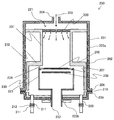
図1は、本実施の形態における半導体製造装置の模式的な断面図である。 FIG. 1 is a schematic cross-sectional view of a semiconductor manufacturing apparatus in the present embodiment.
図1の半導体製造装置200において、201は成膜室としてのチャンバ、202はチャンバ内壁を被覆して保護する中空筒状のライナ、203a、203bはチャンバを冷却する冷却水の流路、204はプロセスガス225を導入する供給部、205は反応後のプロセスガスの排気部、206は気相成長を行うウェハ等の半導体基板、207は半導体基板206を支持するサセプタ、208は図示しない支持部に支持されて半導体基板206を加熱するヒータ、209はチャンバ201の上下部を連結するフランジ部、210はフランジ部209をシールするパッキン、211は排気部205と配管を連結するフランジ部、212はフランジ部211をシールするパッキンである。
In the
ヒータ208としては、SiC材料を用いて構成された抵抗加熱用のヒータが用いられる。尚、ヒータ208の形状は図1の構造に限定されるものではなく、また、インヒータとアウトヒータの2種類のヒータによって加熱するようにしてもよい。
As the
ライナ202は、通常は、石英製であって透明性を備える。ライナ202の頭部231の上部開口部には、半導体基板206の表面に対してプロセスガス225を均一に供給するためのガス整流板であるシャワープレート220が取り付けられている。
The
チャンバ201の底部には、チャンバ201の内部まで伸びる回転軸222が設けられている。回転軸222の上端には回転筒223が配設され、この回転筒223に上述のサセプタ207が取り付けられている。これにより、サセプタ207は、ヒータ208の上方のチャンバ201の内部で回転可能に配置されている。かかる回転機構により、半導体基板206を高速で回転させながら、半導体基板206上にエピタキシャル膜を形成する。この方法によれば、均一に加熱された半導体基板206の表面に新たなプロセスガスが次々に接触するので成膜速度の向上が図れる。
A
また、図1に示す半導体製造装置200においては、シャワープレート220の貫通孔221が半導体基板206に対応する領域内にあるように配置されている。これにより、供給部204から供給されるプロセスガス225をサセプタ207上の半導体基板206の上に均一に供給することができる。
Further, in the
中空筒状の形状を有するライナ202は、シャワープレート220を支持する頭部231の内径がサセプタ207の配置された胴部230より小さくなるよう構成されている。すなわち、中空筒状の形状を有するライナ202は、半導体基板206の配置される胴部230に対して、シャワープレート220を上部にて支持するとともに、シャワープレート220を通過したプロセスガス225の流路となる頭部231の内径が小さくなっている。つまり、ライナ202は、所謂、胴部230に対して頭部231の断面積が絞られた構造を有していることになる。
The
上記構造とすることで、シャワープレート220の貫通孔221を出たプロセスガス225が拡散する無駄な空間を低減することができる。これにより、シャワープレート220から供給されるプロセスガス225が無駄なく半導体基板206の表面に集められ、プロセスガス225の効率的な利用が可能となる。
With the above structure, it is possible to reduce a useless space where the
供給部204からチャンバ201内に供給されたプロセスガス225は、頭部231を通過して半導体基板206の表面に向かって効率よく流下する。このとき、半導体基板206表面でのプロセスガス225の流れをより均一にするよう、半導体基板206の周縁部分とライナ202との間の隙間は狭くなっている。具体的には、ライナ202の頭部231と胴部230との境にある、段部232の角部234と半導体基板206の周縁部分との間の隙間が狭くなっている。
The
半導体製造装置200では、チャンバ201内でサセプタ207により半導体基板206が支持される。そして、回転軸222によって半導体基板206をサセプタ207を介して回転させながら、ヒータ208を用いて半導体基板206を1000℃以上に加熱する。この状態でチャンバ201内に反応ガスを含むプロセスガス225を、供給部204からシャワープレート220の貫通孔221を介して供給する。
In the
すると、半導体基板206表面で熱分解反応または水素還元反応が起こり、半導体基板206の表面にエピタキシャル膜が形成される。その際、気相成長反応に使用されたもの以外のプロセスガスは、変性された生成ガスとなり、プロセスガス225とともにチャンバ201下部に設けられた排気部205から逐次排気される。
Then, a thermal decomposition reaction or a hydrogen reduction reaction occurs on the surface of the
本実施の形態では、チャンバ201内において、半導体基板206上へのSiCエピタキシャル膜の形成を行う。具体的には、サセプタ207上に半導体基板206を載置し、半導体基板206を加熱するとともに、サセプタ207を介して半導体基板206を回転させる。この状態で半導体基板206の表面に反応ガスを接触させることで、半導体基板206の表面にSiCエピタキシャル膜を形成する。
In the present embodiment, a SiC epitaxial film is formed on the
半導体基板206としては、例えば、SiCウェハまたはSiウェハを用いることができる。あるいは、SiO2(石英)ウェハなどの他の絶縁性基板や、GaAs(ガリウム砒素)ウェハなどの高抵抗の半絶縁性基板などを用いることも可能である。
As the
SiCをエピタキシャル成長させるには、半導体基板206を1500℃以上の温度まで昇温する必要がある。このため、サセプタ207には高耐熱性の材料を用いる必要があり、具体的には、等方性黒鉛の表面にCVD(Chemical Vapor Deposition)法によってSiCを被覆したものなどが用いられる。サセプタ207の形状は、半導体基板206を載置可能な形状であれば特に限定されるものではなく、リング状や円盤状など適宜選択して用いられる。
In order to epitaxially grow SiC, it is necessary to raise the temperature of the
反応ガスとしては、例えば、シラン(SiH4)やジクロロシラン(SiH2Cl2)などの珪素(Si)のソースガスと、プロパン(C3H8)やアセチレン(C2H2)などの炭素(C)のソースガスと、キャリアガスとしての水素(H2)ガスとを混合させた混合ガスが導入される。 Examples of the reaction gas include silicon (Si) source gas such as silane (SiH 4 ) and dichlorosilane (SiH 2 Cl 2 ), and carbon such as propane (C 3 H 8 ) and acetylene (C 2 H 2 ). A mixed gas obtained by mixing the source gas (C) and hydrogen (H 2 ) gas as a carrier gas is introduced.
尚、チャンバ201の上部には、供給部204とは別に、キャリアガスである水素ガスをチャンバ201内に供給するための水素ガス供給部をさらに設けることも可能である。その場合、供給部204から炭素(C)のソースガスを含むガス、例えばアセチレンを供給し、水素ガス供給部からキャリアガスである水素ガスを供給し、チャンバ201内で混合して半導体基板206の表面に供給する。
Note that a hydrogen gas supply unit for supplying hydrogen gas as a carrier gas into the
上記の通り、SiCエピタキシャル成長工程では、半導体基板206を非常に高温にする必要がある。しかし、半導体基板206を高温の状態にするためにヒータ208で加熱すると、ヒータ208からの輻射熱は、半導体基板206だけでなく、チャンバ201を構成する他の部材にも伝わってそれらを昇温させてしまう。こうしたことは、特に、半導体基板206やヒータ208のような高温となる部分の近傍に位置する部材や、チャンバ201の内壁あるいは配管において顕著である。そして、チャンバ201内に生じた高温部位に反応ガスが接触すると、高温加熱された半導体基板206の表面と同様に反応ガスの熱分解反応が起こる。
As described above, in the SiC epitaxial growth process, the
例えば、半導体基板206の表面にSiCエピタキシャル膜を形成しようとする場合、反応ガスとして、Si源としてのシラン(SiH4)、C源としてのプロパン(C3H8)、キャリアガスとしての水素ガスなどを含んで調製された混合ガスが用いられる。反応ガスは、供給部204を通じてチャンバ201の上部からチャンバ201内に供給され、高温加熱された半導体基板206の表面に到達して分解する。
For example, when an SiC epitaxial film is to be formed on the surface of the
しかしながら、上記組成の反応ガスは、反応性に富んでいるために、一定の温度条件を満たす部材に接触すると、半導体基板206上でなくとも分解反応を起こしてしまう。その結果、チャンバ201内の部材、具体的には、サセプタ207、チャンバ201の内壁、チャンバ201内のガスを排気する配管などに、反応ガスに由来する多結晶のSiC膜が付着する。この膜が剥離するとダストとなり、半導体基板206上に形成されるエピタキシャル膜に欠陥を生じさせるので、付着した膜をクリーニング除去する作業が必要になる。尚、この付着した膜は、サセプタ207やチャンバ201の内壁の構成物である緻密な多結晶のSiC膜とは異なり、緻密でない多結晶のSiC膜と考えられる。ここで、緻密な多結晶とは、緻密でない多結晶に比べて多結晶の中で単結晶に近いことを意味する。
However, since the reaction gas having the above composition is rich in reactivity, when it comes into contact with a member that satisfies a certain temperature condition, a decomposition reaction occurs even if it is not on the
本実施の形態では、以下のようにしてサセプタ207に付着したSiC膜を除去する。
In the present embodiment, the SiC film attached to
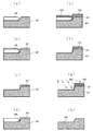
図2(a)〜(h)は、本実施の形態におけるサセプタの処理方法を説明する図である。 2A to 2H are views for explaining a susceptor processing method according to the present embodiment.
SiC膜の成膜に際しては、まず、チャンバ201内に半導体基板(ウェハ)206を搬送し、サセプタ207の上に載置する。ここで、本実施の形態においては、半導体基板206を搬送する前にチャンバ201内に別の基板(ダミーウェハ)106を搬送し、図2(a)に示すように、この基板106をサセプタ207の上に載置する。基板106について、半導体基板206と同種のものであるか否かは問わない。
In forming the SiC film, first, the semiconductor substrate (wafer) 206 is transferred into the
次に、基板106の上にSi膜301を形成する。Si膜301の20μm〜50μmとすることが好ましい。Si膜301は、後工程で除去されるものであることから、あまり厚くすることは、コストの点から適当でない。一方、薄すぎると、膜としての特性を備えることができず、後述する本発明の効果が得られなくなる。
Next, a
例えば、基板106としてシリコンウェハを用い、これをサセプタ207の上に載置する。次いで、常圧下または適当な減圧下で水素ガスを流しながら、サセプタ207に付随させて、シリコンウェハを50rpm程度で回転させる。次に、ヒータ208によってシリコンウェハを1100℃〜1200℃に加熱する。放射温度計(図示せず)による測定でシリコンウェハの温度が1150℃に達したことを確認した後は、徐々にシリコンウェハの回転数を上げていく。そして、供給部204からシャワープレート220を介して原料ガスをチャンバ201の内部に供給する。原料ガスとしては、トリクロロシランを用いることができ、キャリアガスとしての水素ガスと混合した状態で、供給部204からチャンバ201の内部に導入する。チャンバ201の内部に導入された原料ガスは、シリコンウェハの方に流下する。そして、シリコンウェハの温度を1150℃に維持し、サセプタ207を900rpm以上の高速で回転させながら、供給部204からシャワープレート220を介して次々に新たな原料ガスをシリコンウェハに供給する。これにより、シリコンウェハの上に均一な厚さのシリコンエピタキシャル膜を成長させることができる。
For example, a silicon wafer is used as the
基板106の上にSi膜を形成する工程では、図2(b)に示すように、サセプタ207の上にもSi膜301が形成される。
In the step of forming the Si film on the
Si膜301の形成後、サセプタ207上から基板106を除去すると、図2(c)に示すようになる。図2(c)において、サセプタ207上の基板106が載置されていた部分にはSi膜が形成されていない。換言すると、図2(a)〜(c)に示す工程は、SiC膜の形成時に基板によって被覆されないサセプタ207の表面にSi膜を形成する工程である。
When the
次に、SiC膜302の形成工程を行う。この工程は、通常のSiCエピタキシャルウェハの製造工程と同様である。SiC膜302の膜厚は、通常、50μm〜100μm程度である。
Next, a process for forming the
まず、チャンバ201から基板106を搬出した後、半導体基板206をチャンバ201内に搬送する。そして、図2(d)に示すように、サセプタ207上に半導体基板206を載置する。
First, after the
次に、サセプタ207に付随させて、サセプタ207上に載置された半導体基板206を50rpm程度で回転させる。
Next, in association with the
ヒータ208に電流を供給して作動させ、ヒータ208から発せられる熱によって半導体基板206を加熱する。半導体基板206の温度が、成膜温度である1500℃〜1700℃までの間の所定の温度、例えば、1650℃に達するまで徐々に加熱する。このとき、チャンバ201の壁部分に設けた流路203a、203bに冷却水を流すことで、過度にチャンバ201が昇温するのを防止できる。
An electric current is supplied to the
半導体基板206の温度が1650℃に達した後は、ヒータ208により1650℃近辺での緻密な温度調整がなされる。このとき、半導体基板206の温度は、放射温度計を用いて測定することができる。
After the temperature of the
放射温度計による測定で半導体基板206の温度が所定温度に達したことを確認した後は、徐々に半導体基板206の回転数を上げていく。例えば、900rpm程度の回転数とするのがよい。
After confirming that the temperature of the
また、供給部204から反応ガスを含むプロセスガス225を供給し、シャワープレート220を介して、プロセスガス225を半導体基板206の上に流下させる。このとき、プロセスガス225は、整流板であるシャワープレート220を通過して整流され、下方の半導体基板206に向かってほぼ鉛直に流下して、いわゆる縦フローを形成する。
Further, the
プロセスガス225としては、例えば、シラン(SiH4)やジクロロシラン(SiH2Cl2)などの珪素(Si)のソースガスと、プロパン(C3H8)やアセチレン(C2H2)などの炭素(C)のソースガスと、キャリアガスとしての水素(H2)ガスとを混合させた混合ガスを使用する。
Examples of the
半導体基板206の表面に到達したプロセスガス225は、熱分解反応または水素還元反応を起こす。これにより、半導体基板206の表面にSiC膜が形成される。プロセスガス225の内で気相成長反応に使用されたもの以外のガスは、変性された生成ガスとなり、チャンバ201の下部に設けられた排気部205から排気される。
The
半導体基板206の上に、所定の膜厚のSiC膜302を形成した後は、プロセスガス225の供給を終了する。そして、半導体基板206が所定の温度まで冷却されたのを確認してから、チャンバ201の外部に半導体基板206を搬出する。
After the
図2(e)は、半導体基板206の上にSiC膜302が形成された状態を示している。ここで、SiC膜302は、サセプタ207の表面、正確には、サセプタ207上に形成されたSi膜301の上にも形成されている。
FIG. 2E shows a state in which the
図2(f)は、サセプタ207の上から半導体基板206を除去した後の状態を示している。この図から分かるように、半導体基板206が載置されていた部分には、SiC膜302が形成されていない。
FIG. 2 (f) shows a state after the
次に、サセプタ207の表面に付着したSiC膜302をSi膜301とともに除去する。
Next, the
まず、サセプタ207を回転させながら、ヒータ208から発せられる熱によってサセプタ207を加熱する。サセプタ207の回転数は、例えば、400rpm〜1000rpmとすることができる。また、サセプタ207の加熱温度は、例えば、1000℃〜1200℃とすることができる。但し、エッチング処理の際のサセプタ207の回転数と温度の管理には、成膜処理における管理ほどの厳密性は要求されない。
First, the
次に、供給路204からエッチングガスを導入し、図2(g)に示すように、サセプタ207に向けてエッチングガスを流下させる。エッチングガスとしては、例えば、H2ガスで希釈した50%濃度のHClガスを用いることができる。
Next, an etching gas is introduced from the
ここで、サセプタ207に設けられている段差部303からは、Si膜301の一部が露出している。この原因としては、段差部303において、Si膜301を完全に被覆するようにSiC膜302を形成するのが難しいことが挙げられる。Si膜301やSiC膜302の成膜時において、段差部303には基板106または半導体基板206が近接しており、基板106と半導体基板206とが完全に同じ位置に載置されない可能性があることを考えれば、SiC膜302によって覆われていないSi膜301が存在するのは当然とも言える。
Here, a part of the
サセプタ207が加熱された状態でHClガスが導入されると、段差部303から露出しているSi膜301とHClガスとが反応してSixCly化合物が形成される。このSixCly化合物は、サセプタ207が回転していることにより、SiC膜302とともにエッチングガスの流れに乗り、サセプタ207の周縁部から排気部205を通じて排出される。つまり、この方法によれば、Si膜301と一緒にSiC膜302を除去することができる。HClガスによってSiC膜302はエッチングされないが、下層のSi膜301がエッチングされるために、結果としてサセプタ207上からSiC膜302を除去できるのである。尚、HClガスによりエッチングできるものであれば、Si膜301に代えてSiGe膜やその他のシリコン化合物膜とすることも可能である。
When the HCl gas in the state in which the
HClガスによるエッチング処理の終了は、時間で管理することができる。図2(h)は、エッチング終了後のサセプタ207の表面を模式的に表した図である。この図に示すように、本実施の形態によれば、HClガスを用いたエッチングによって、サセプタ207の表面に付着したSiC膜302を除去することができる。
The completion of the etching process using HCl gas can be managed by time. FIG. 2H schematically shows the surface of the
本実施の形態における基板106としては、半導体基板206と同じ大きさのものを用いることが好ましい。但し、半導体基板206より小さい場合であっても本発明の効果は得られる。この場合、図2(d)において、半導体基板206の下にSi膜301が形成されている部分があることになる。半導体基板206上へのSiC膜302の形成を終えた後、すなわち、図2(f)においては、SiC膜302によって被覆されていないSi膜301が存在する。しかし、このSi膜301は、図2(g)のHClガスによるエッチングによって除去されるので、結果として、図2(h)に示す状態のサセプタ207を得ることができる。
As the
一方、基板106として半導体基板206より大きいものを用いた場合には、次のようになる。この場合、図2(d)において、半導体基板206から露出しているサセプタ207の表面にSi膜301によって被覆されていない箇所が存在する。このことは、半導体基板206上へのSiC膜302の形成過程で、サセプタ207の表面に直接SiC膜302が形成される箇所が生じることを意味する。この箇所におけるSiC膜302は、図2(g)のHClガスによるエッチングでは除去されない。したがって、半導体基板206と同じ大きさ、または、これより小さい基板106を用いた場合と同じ効果は得られ難い。しかしながら、以下に述べるClF3ガスを用いたエッチングによって除去可能である。
On the other hand, when a
本実施の形態においては、HClガスを用いてのエッチングの後に、チャンバ201内に少量のClF3ガスを導入することが好ましい。これは、Si膜301と一緒に除去されるSiC膜302の一部がチャンバ201内に残留するのを防ぐためである。また、このエッチングによって、半導体基板206より大きい基板106を用いた場合に、HClガスによっては除去されなかったサセプタ207上のSiC膜302を除去することもできる。但し、サセプタ207やチャンバ201の内壁を構成するSiC膜へのエッチングを防ぐために、ClF3ガスの導入は、低温且つ短時間に留める必要がある。例えば、ClF3ガスによるエッチング工程は、ヒータ208の電源をオフとした後の余熱下で行うことができる。また、HClガスによるエッチング時間が30分である場合、ClF3ガスによるエッチングは3分とすることができる。
In this embodiment mode, it is preferable to introduce a small amount of ClF 3 gas into the
ClF3ガスによるエッチング処理の終了も時間で管理することができる。上述の通り、サセプタ207の表面に付着するSiC膜は、サセプタ207を構成する緻密な多結晶のSiC膜(黒鉛の表面にコートされたSiC膜)とは異なり、緻密でない多結晶の膜と考えられる。この緻密でない多結晶のSiC膜のエッチングレートは、緻密な多結晶のSiC膜に比較して十分速くなると予想される。しかしながら、これらは、同一成分であるので、100%ClF3ガスを用いた場合の選択比は十分でない。
The completion of the etching process using ClF 3 gas can also be managed by time. As described above, the SiC film adhering to the surface of the
そこで、エッチング処理には、窒素ガスで希釈した10%〜20%濃度のClF3ガスをエッチングガスとして用いることが好ましい。単結晶のSiC膜のエッチングには、通常、100%ClF3ガスが使用されるが、この場合は、希釈したClF3ガスを用いることで、緻密な多結晶のSiC膜と、緻密でない多結晶のSiC膜との間のエッチングレートに明確な差を設けることができる。 Therefore, for the etching process, it is preferable to use ClF 3 gas having a concentration of 10% to 20% diluted with nitrogen gas as an etching gas. For etching a single crystal SiC film, 100% ClF 3 gas is usually used. In this case, by using diluted ClF 3 gas, a dense polycrystalline SiC film and a non-dense polycrystalline film are used. A clear difference can be provided in the etching rate with the SiC film.
チャンバ201内にClF3ガスが供給されると、下記式(1)にしたがってSiCと反応する(Y.Miura, H.Habuka, Y.Katsumi, S.Oda, Y.Fukai, K.Fukae, T.Kato, H.Okumura, K.Arai, Japanese Journal of Applied Physics. Vol.46, No.12, 2007, pp.7875−7879)。この反応により、チャンバ201内に残存するSiC膜がエッチング除去される。
3SiC+8ClF3 → 3SiF4+3CF4+4Cl2 (1)
When ClF 3 gas is supplied into the
3SiC + 8ClF 3 → 3SiF 4 + 3CF 4 + 4Cl 2 (1)
以上述べたように、本実施の形態のサセプタの処理方法および半導体製造装置の処理方法によれば、ClF3ガスを使用せずにサセプタに付着したSiC膜を除去することができる。 As described above, according to the susceptor processing method and the semiconductor manufacturing apparatus processing method of the present embodiment, the SiC film adhering to the susceptor can be removed without using ClF 3 gas.
尚、本発明は上記実施の形態に限定されるものではなく、本発明の趣旨を逸脱しない範囲内で種々変形して実施することができる。 The present invention is not limited to the above-described embodiment, and various modifications can be made without departing from the spirit of the present invention.
200 半導体製造装置
201 チャンバ
202 ライナ
203a、203b 流路
204 供給部
205 排気部
206 半導体基板
207 サセプタ
208 ヒータ
209、211 フランジ部
210、212 パッキン
220 シャワープレート
221 貫通孔
222 回転軸
223 回転筒
225 プロセスガス
230 胴部
231 頭部
232 段部
234 角部
106 基板
301 Si膜
302 SiC膜
303 段差部
DESCRIPTION OF
Claims (5)
前記サセプタの上に前記第1の基板に代えて第2の基板を載置し、該第2の基板の上にSiC膜をエピタキシャル成長させる工程と、
前記第2の基板が取り除かれた前記サセプタを所定の温度に加熱し回転させながら、前記サセプタの上方からHClガスを流下させて、前記サセプタ上のSi膜およびSiC膜を除去する工程とを有することを特徴とするサセプタの処理方法。 Placing a first substrate on a susceptor and epitaxially growing a Si film on the first substrate;
Placing a second substrate on the susceptor instead of the first substrate, and epitaxially growing a SiC film on the second substrate;
A step of removing the Si film and the SiC film on the susceptor by causing HCl gas to flow from above the susceptor while heating and rotating the susceptor from which the second substrate has been removed to a predetermined temperature. And a susceptor processing method.
前記サセプタが配置されて前記ウェハの上にエピタキシャル膜を形成する成膜室とを備えた半導体製造装置の処理方法であって、
前記成膜室において、前記サセプタの上にダミーウェハを載置し、該ダミーウェハの上にSi膜をエピタキシャル成長させた後、前記サセプタの上に前記ダミーウェハに代えて前記ウェハを載置し、該ウェハの上にSiC膜をエピタキシャル成長させ、次いで、前記サセプタから前記ウェハを取り除いた後、前記サセプタを所定の温度に加熱し回転させながら、前記サセプタの上方からHClガスを流下させて、前記サセプタ上のSi膜およびSiC膜を除去することを特徴とする半導体製造装置の処理方法。 A susceptor on which the wafer is placed;
A processing method of a semiconductor manufacturing apparatus including a film forming chamber in which the susceptor is disposed to form an epitaxial film on the wafer,
In the film formation chamber, a dummy wafer is placed on the susceptor, and after an Si film is epitaxially grown on the dummy wafer, the wafer is placed on the susceptor instead of the dummy wafer. An SiC film is epitaxially grown on the susceptor, and after removing the wafer from the susceptor, HCl gas is allowed to flow from above the susceptor while rotating and heating the susceptor to a predetermined temperature. A method of processing a semiconductor manufacturing apparatus, comprising removing the film and the SiC film.
Priority Applications (2)
| Application Number | Priority Date | Filing Date | Title |
|---|---|---|---|
| JP2010172962A JP5479260B2 (en) | 2010-07-30 | 2010-07-30 | Susceptor processing method and semiconductor manufacturing apparatus processing method |
| US13/170,867 US8334214B2 (en) | 2010-07-30 | 2011-06-28 | Susceptor treatment method and a method for treating a semiconductor manufacturing apparatus |
Applications Claiming Priority (1)
| Application Number | Priority Date | Filing Date | Title |
|---|---|---|---|
| JP2010172962A JP5479260B2 (en) | 2010-07-30 | 2010-07-30 | Susceptor processing method and semiconductor manufacturing apparatus processing method |
Publications (2)
| Publication Number | Publication Date |
|---|---|
| JP2012033775A JP2012033775A (en) | 2012-02-16 |
| JP5479260B2 true JP5479260B2 (en) | 2014-04-23 |
Family
ID=45527166
Family Applications (1)
| Application Number | Title | Priority Date | Filing Date |
|---|---|---|---|
| JP2010172962A Active JP5479260B2 (en) | 2010-07-30 | 2010-07-30 | Susceptor processing method and semiconductor manufacturing apparatus processing method |
Country Status (2)
| Country | Link |
|---|---|
| US (1) | US8334214B2 (en) |
| JP (1) | JP5479260B2 (en) |
Families Citing this family (9)
| Publication number | Priority date | Publication date | Assignee | Title |
|---|---|---|---|---|
| JP5732284B2 (en) * | 2010-08-27 | 2015-06-10 | 株式会社ニューフレアテクノロジー | Film forming apparatus and film forming method |
| JP5719720B2 (en) * | 2011-08-19 | 2015-05-20 | 株式会社ニューフレアテクノロジー | Thin film processing method |
| WO2014062000A1 (en) * | 2012-10-16 | 2014-04-24 | 주식회사 엘지실트론 | Susceptor for epitaxial growing and method for epitaxial growing |
| KR101496572B1 (en) * | 2012-10-16 | 2015-02-26 | 주식회사 엘지실트론 | Susceptor for Epitaxial Growth And Epitaxial Growth Method |
| WO2015119744A1 (en) * | 2014-02-07 | 2015-08-13 | Applied Materials, Inc. | Chucking capability for bowed wafers on dsa |
| US9864532B2 (en) * | 2015-06-26 | 2018-01-09 | International Business Machines Corporation | Performing preprocessing operations in anticipation of log file writes |
| JP6967403B2 (en) | 2017-08-30 | 2021-11-17 | 株式会社ニューフレアテクノロジー | Vapor deposition method |
| KR102641135B1 (en) * | 2019-12-16 | 2024-02-28 | 가부시키가이샤 후지킨 | Vaporization supply method and vaporization supply device |
| CN117480590B (en) * | 2021-05-13 | 2026-01-09 | 环球晶圆股份有限公司 | Methods for etching semiconductor structures and for regulating processing reactors |
Family Cites Families (3)
| Publication number | Priority date | Publication date | Assignee | Title |
|---|---|---|---|---|
| US20060065634A1 (en) * | 2004-09-17 | 2006-03-30 | Van Den Berg Jannes R | Low temperature susceptor cleaning |
| JP2007073628A (en) | 2005-09-05 | 2007-03-22 | Nuflare Technology Inc | Semiconductor manufacturing apparatus and semiconductor manufacturing method |
| JP5010235B2 (en) | 2006-10-26 | 2012-08-29 | 株式会社ニューフレアテクノロジー | Vapor growth method |
-
2010
- 2010-07-30 JP JP2010172962A patent/JP5479260B2/en active Active
-
2011
- 2011-06-28 US US13/170,867 patent/US8334214B2/en active Active
Also Published As
| Publication number | Publication date |
|---|---|
| JP2012033775A (en) | 2012-02-16 |
| US8334214B2 (en) | 2012-12-18 |
| US20120028445A1 (en) | 2012-02-02 |
Similar Documents
| Publication | Publication Date | Title |
|---|---|---|
| JP5479260B2 (en) | Susceptor processing method and semiconductor manufacturing apparatus processing method | |
| JP5698043B2 (en) | Semiconductor manufacturing equipment | |
| JP5542560B2 (en) | Semiconductor manufacturing apparatus and susceptor cleaning method | |
| JP5372816B2 (en) | Film forming apparatus and film forming method | |
| JP5542584B2 (en) | Film forming apparatus and film forming method | |
| JP2008060545A (en) | Semiconductor manufacturing apparatus and semiconductor manufacturing method | |
| US9194056B2 (en) | Film-forming apparatus and method | |
| JP2011171450A (en) | Film deposition apparatus and method | |
| JP2013030758A (en) | Film formation device and film formation method | |
| WO2006137192A1 (en) | Method of surface reconstruction for silicon carbide substrate | |
| JP5496721B2 (en) | Film forming apparatus and film forming method | |
| JP5719720B2 (en) | Thin film processing method | |
| KR20130044789A (en) | Apparatus, method for fabrication epi wafer and epi wafer | |
| JP5719710B2 (en) | Vapor growth apparatus and vapor growth method | |
| JP5896346B2 (en) | Silicon carbide semiconductor | |
| JP2015122540A5 (en) | ||
| JP5264384B2 (en) | Vapor growth apparatus and vapor growth method | |
| JP2013016562A (en) | Vapor-phase growth method | |
| JP5757748B2 (en) | Semiconductor manufacturing apparatus and semiconductor manufacturing method | |
| JP2013045799A (en) | Film formation device and film formation method | |
| JP5736291B2 (en) | Film forming apparatus and film forming method | |
| JP5807505B2 (en) | Epitaxial wafer manufacturing method | |
| JP5252896B2 (en) | Vapor growth apparatus and vapor growth method | |
| JP2019169689A (en) | Deposition apparatus and deposition method | |
| JP2022121078A (en) | Susceptor, deposition apparatus, and substrate deposition method |
Legal Events
| Date | Code | Title | Description |
|---|---|---|---|
| A711 | Notification of change in applicant |
Free format text: JAPANESE INTERMEDIATE CODE: A711 Effective date: 20121106 |
|
| A621 | Written request for application examination |
Free format text: JAPANESE INTERMEDIATE CODE: A621 Effective date: 20130517 |
|
| RD03 | Notification of appointment of power of attorney |
Free format text: JAPANESE INTERMEDIATE CODE: A7423 Effective date: 20130806 |
|
| A521 | Request for written amendment filed |
Free format text: JAPANESE INTERMEDIATE CODE: A821 Effective date: 20130806 |
|
| A977 | Report on retrieval |
Free format text: JAPANESE INTERMEDIATE CODE: A971007 Effective date: 20140114 |
|
| TRDD | Decision of grant or rejection written | ||
| A01 | Written decision to grant a patent or to grant a registration (utility model) |
Free format text: JAPANESE INTERMEDIATE CODE: A01 Effective date: 20140117 |
|
| A61 | First payment of annual fees (during grant procedure) |
Free format text: JAPANESE INTERMEDIATE CODE: A61 Effective date: 20140212 |
|
| R150 | Certificate of patent or registration of utility model |
Ref document number: 5479260 Country of ref document: JP Free format text: JAPANESE INTERMEDIATE CODE: R150 |
|
| R250 | Receipt of annual fees |
Free format text: JAPANESE INTERMEDIATE CODE: R250 |
|
| R250 | Receipt of annual fees |
Free format text: JAPANESE INTERMEDIATE CODE: R250 |
|
| R250 | Receipt of annual fees |
Free format text: JAPANESE INTERMEDIATE CODE: R250 |
|
| R250 | Receipt of annual fees |
Free format text: JAPANESE INTERMEDIATE CODE: R250 |
|
| R250 | Receipt of annual fees |
Free format text: JAPANESE INTERMEDIATE CODE: R250 |
|
| R250 | Receipt of annual fees |
Free format text: JAPANESE INTERMEDIATE CODE: R250 |
|
| R250 | Receipt of annual fees |
Free format text: JAPANESE INTERMEDIATE CODE: R250 |
|
| R250 | Receipt of annual fees |
Free format text: JAPANESE INTERMEDIATE CODE: R250 |
|
| R250 | Receipt of annual fees |
Free format text: JAPANESE INTERMEDIATE CODE: R250 |
|
| R250 | Receipt of annual fees |
Free format text: JAPANESE INTERMEDIATE CODE: R250 |