JP5537996B2 - 半導体装置 - Google Patents
半導体装置 Download PDFInfo
- Publication number
- JP5537996B2 JP5537996B2 JP2010046394A JP2010046394A JP5537996B2 JP 5537996 B2 JP5537996 B2 JP 5537996B2 JP 2010046394 A JP2010046394 A JP 2010046394A JP 2010046394 A JP2010046394 A JP 2010046394A JP 5537996 B2 JP5537996 B2 JP 5537996B2
- Authority
- JP
- Japan
- Prior art keywords
- semiconductor region
- region
- buried
- semiconductor
- layer
- Prior art date
- Legal status (The legal status is an assumption and is not a legal conclusion. Google has not performed a legal analysis and makes no representation as to the accuracy of the status listed.)
- Expired - Fee Related
Links
Images





Classifications
-
- H—ELECTRICITY
- H10—SEMICONDUCTOR DEVICES; ELECTRIC SOLID-STATE DEVICES NOT OTHERWISE PROVIDED FOR
- H10D—INORGANIC ELECTRIC SEMICONDUCTOR DEVICES
- H10D30/00—Field-effect transistors [FET]
- H10D30/60—Insulated-gate field-effect transistors [IGFET]
- H10D30/64—Double-diffused metal-oxide semiconductor [DMOS] FETs
- H10D30/66—Vertical DMOS [VDMOS] FETs
- H10D30/665—Vertical DMOS [VDMOS] FETs having edge termination structures
-
- H—ELECTRICITY
- H10—SEMICONDUCTOR DEVICES; ELECTRIC SOLID-STATE DEVICES NOT OTHERWISE PROVIDED FOR
- H10D—INORGANIC ELECTRIC SEMICONDUCTOR DEVICES
- H10D48/00—Individual devices not covered by groups H10D1/00 - H10D44/00
- H10D48/30—Devices controlled by electric currents or voltages
- H10D48/32—Devices controlled by only the electric current supplied, or only the electric potential applied, to an electrode which does not carry the current to be rectified, amplified or switched
- H10D48/34—Bipolar devices
- H10D48/345—Bipolar transistors having ohmic electrodes on emitter-like, base-like, and collector-like regions
-
- H—ELECTRICITY
- H10—SEMICONDUCTOR DEVICES; ELECTRIC SOLID-STATE DEVICES NOT OTHERWISE PROVIDED FOR
- H10D—INORGANIC ELECTRIC SEMICONDUCTOR DEVICES
- H10D62/00—Semiconductor bodies, or regions thereof, of devices having potential barriers
- H10D62/01—Manufacture or treatment
- H10D62/051—Forming charge compensation regions, e.g. superjunctions
- H10D62/054—Forming charge compensation regions, e.g. superjunctions by high energy implantations in bulk semiconductor bodies, e.g. forming pillars
-
- H—ELECTRICITY
- H10—SEMICONDUCTOR DEVICES; ELECTRIC SOLID-STATE DEVICES NOT OTHERWISE PROVIDED FOR
- H10D—INORGANIC ELECTRIC SEMICONDUCTOR DEVICES
- H10D62/00—Semiconductor bodies, or regions thereof, of devices having potential barriers
- H10D62/10—Shapes, relative sizes or dispositions of the regions of the semiconductor bodies; Shapes of the semiconductor bodies
- H10D62/102—Constructional design considerations for preventing surface leakage or controlling electric field concentration
- H10D62/103—Constructional design considerations for preventing surface leakage or controlling electric field concentration for increasing or controlling the breakdown voltage of reverse-biased devices
- H10D62/105—Constructional design considerations for preventing surface leakage or controlling electric field concentration for increasing or controlling the breakdown voltage of reverse-biased devices by having particular doping profiles, shapes or arrangements of PN junctions; by having supplementary regions, e.g. junction termination extension [JTE]
- H10D62/106—Constructional design considerations for preventing surface leakage or controlling electric field concentration for increasing or controlling the breakdown voltage of reverse-biased devices by having particular doping profiles, shapes or arrangements of PN junctions; by having supplementary regions, e.g. junction termination extension [JTE] having supplementary regions doped oppositely to or in rectifying contact with regions of the semiconductor bodies, e.g. guard rings with PN or Schottky junctions
-
- H—ELECTRICITY
- H10—SEMICONDUCTOR DEVICES; ELECTRIC SOLID-STATE DEVICES NOT OTHERWISE PROVIDED FOR
- H10D—INORGANIC ELECTRIC SEMICONDUCTOR DEVICES
- H10D62/00—Semiconductor bodies, or regions thereof, of devices having potential barriers
- H10D62/10—Shapes, relative sizes or dispositions of the regions of the semiconductor bodies; Shapes of the semiconductor bodies
- H10D62/102—Constructional design considerations for preventing surface leakage or controlling electric field concentration
- H10D62/103—Constructional design considerations for preventing surface leakage or controlling electric field concentration for increasing or controlling the breakdown voltage of reverse-biased devices
- H10D62/105—Constructional design considerations for preventing surface leakage or controlling electric field concentration for increasing or controlling the breakdown voltage of reverse-biased devices by having particular doping profiles, shapes or arrangements of PN junctions; by having supplementary regions, e.g. junction termination extension [JTE]
- H10D62/106—Constructional design considerations for preventing surface leakage or controlling electric field concentration for increasing or controlling the breakdown voltage of reverse-biased devices by having particular doping profiles, shapes or arrangements of PN junctions; by having supplementary regions, e.g. junction termination extension [JTE] having supplementary regions doped oppositely to or in rectifying contact with regions of the semiconductor bodies, e.g. guard rings with PN or Schottky junctions
- H10D62/107—Buried supplementary regions, e.g. buried guard rings
-
- H—ELECTRICITY
- H10—SEMICONDUCTOR DEVICES; ELECTRIC SOLID-STATE DEVICES NOT OTHERWISE PROVIDED FOR
- H10D—INORGANIC ELECTRIC SEMICONDUCTOR DEVICES
- H10D62/00—Semiconductor bodies, or regions thereof, of devices having potential barriers
- H10D62/10—Shapes, relative sizes or dispositions of the regions of the semiconductor bodies; Shapes of the semiconductor bodies
- H10D62/102—Constructional design considerations for preventing surface leakage or controlling electric field concentration
- H10D62/103—Constructional design considerations for preventing surface leakage or controlling electric field concentration for increasing or controlling the breakdown voltage of reverse-biased devices
- H10D62/105—Constructional design considerations for preventing surface leakage or controlling electric field concentration for increasing or controlling the breakdown voltage of reverse-biased devices by having particular doping profiles, shapes or arrangements of PN junctions; by having supplementary regions, e.g. junction termination extension [JTE]
- H10D62/109—Reduced surface field [RESURF] PN junction structures
- H10D62/111—Multiple RESURF structures, e.g. double RESURF or 3D-RESURF structures
-
- H—ELECTRICITY
- H10—SEMICONDUCTOR DEVICES; ELECTRIC SOLID-STATE DEVICES NOT OTHERWISE PROVIDED FOR
- H10D—INORGANIC ELECTRIC SEMICONDUCTOR DEVICES
- H10D84/00—Integrated devices formed in or on semiconductor substrates that comprise only semiconducting layers, e.g. on Si wafers or on GaAs-on-Si wafers
Landscapes
- Insulated Gate Type Field-Effect Transistor (AREA)
- Electrodes Of Semiconductors (AREA)
Description
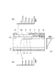
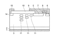
図1は、第1の実施形態を説明するパワーMOSFETの構成の一例を模式的に示す断面図である。このMOSFETでは、第1半導体領域としてn+ドレイン層2の一方の主面(表面)上に第2半導体領域としてnドリフト層3が形成されている。このn+ドレイン層2の一方の主面とは反対側となる他方の主面(裏面)上には、第1の主電極としてのドレイン電極1が形成されている。
図3は、第1の実施形態の他の例(その1)を説明するパワーMOSFETの構成の一例を模式的に示す断面図である。ここでは、図1と同一部分の詳しい説明は省略し、異なる部分についてのみ説明する。
図4は、第1の実施形態の他の例(その2)を説明するパワーMOSFETの構成の一例を模式的に示す断面図である。ここでは、図1と同一部分の詳しい説明は省略し、異なる部分についてのみ説明する。
図5は、第1の実施形態の他の例(その3)を説明するパワーMOSFETの構成の一例を模式的に示す断面図である。ここでは、図1と同一部分の詳しい説明は省略し、異なる部分についてのみ説明する。
図6は、第1の実施形態の他の例(その4)を説明するパワーMOSFETの構成の一例を模式的に示す断面図である。ここでは、図1と同一部分の詳しい説明は省略し、異なる部分についてのみ説明する。
図7は、第2の実施の形態を説明するパワーMOSFETの構成の一例を模式的に示す断面図である。図1と同一部分の詳しい説明は省略し、ここでは異なる部分についてのみ説明する。
図8は、第2の実施形態の他の例(その1)を説明するパワーMOSFETの構成の一例を模式的に示す断面図である。ここでは、図7と同一部分の詳しい説明は省略し、異なる部分についてのみ説明する。
図9は、第2の実施形態の他の例(その2)を説明するパワーMOSFETの構成の一例を模式的に示す断面図である。ここでは、図7と同一部分の詳しい説明は省略し、異なる部分についてのみ説明する。
図10は、第3の実施形態を説明するパワーMOSFETの構成の一例を模式的に示す断面図である。図1と同一部分の詳しい説明は省略し、ここでは異なる部分についてのみ説明する。
図12は、第3の実施形態の他の例(その1)を説明するパワーMOSFETの構成の一例を模式的に示す断面図である。ここでは、図10と同一部分の詳しい説明は省略し、異なる部分についてのみ説明する。
図13は、第3の実施形態の他の例(その2)を説明するパワーMOSFETの構成の一例を模式的に示す断面図である。ここでは、図10と同一部分の詳しい説明は省略し、異なる部分についてのみ説明する。
Claims (5)
- 第1導電型の第1半導体領域と、
前記第1半導体領域の一方の主面上に形成された第1導電型の第2半導体領域と、
前記第1半導体領域の前記一方の主面とは反対側となる他方の主面側に形成された第1の主電極と、
前記第2半導体領域の前記第1半導体領域とは反対側となる主面に選択的に形成された第2導電型の第3半導体領域と、
前記第3半導体領域に接合するよう形成された第2の主電極と、
前記第2半導体領域において前記第1の主電極と前記第2の主電極との間に主電流経路が形成される素子領域の外側となる終端領域に設けられた第2導電型の複数の埋め込み半導体領域と、
を備え、
前記埋め込み半導体領域は、前記素子領域から外側に向かうほど前記第2半導体領域の前記第3半導体領域が形成された主面から遠くなり、
複数の前記埋め込み半導体領域中から任意に選択された第1の埋め込み半導体領域と、前記第1の埋め込み半導体領域よりも前記終端領域側に配置された第2の埋め込み半導体領域と、において、前記第1の埋め込み半導体領域の下には前記第2の埋め込み半導体領域が位置せず、
前記第1の埋め込み半導体領域および前記第2の埋め込み半導体領域は、前記第2半導体領域によって囲まれていることを特徴とする半導体装置。 - 第1導電型の第1半導体領域と、
前記第1半導体領域の一方の主面上に形成された第1導電型の第2半導体領域と、
前記第1半導体領域の前記一方の主面とは反対側となる他方の主面上に形成された第1の主電極と、
前記第2半導体領域の前記第1半導体領域とは反対側となる主面に選択的に形成された第2導電型の第3半導体領域と、
前記第3半導体領域に選択的に形成された第1導電型の第4半導体領域と、
前記第3半導体領域と前記第4半導体領域とに接合するよう形成された第2の主電極と、
前記第3半導体領域、前記第4半導体領域、および前記第2半導体領域の上にかかるゲート絶縁膜を介して形成された制御電極と、
前記第2半導体領域において前記第1の主電極と前記第2の主電極との間に主電流経路が形成される素子領域の外側となる終端領域に設けられた第2導電型の複数の埋め込み半導体領域と、
を備え、
前記埋め込み半導体領域は、前記素子領域から外側に向かうほど前記第2半導体領域の前記第3半導体領域が形成された主面から遠くなり、
複数の前記埋め込み半導体領域中から任意に選択された第1の埋め込み半導体領域と、前記第1の埋め込み半導体領域よりも前記終端領域側に配置された第2の埋め込み半導体領域と、において、前記第1の埋め込み半導体領域の下には前記第2の埋め込み半導体領域が位置せず、
前記第1の埋め込み半導体領域および前記第2の埋め込み半導体領域は、前記第2半導体領域によって囲まれていることを特徴とする半導体装置。 - 前記第2半導体領域内において前記第2半導体領域の主面と垂直な方向に前記第3半導体領域と接続して形成され、前記主面の方向に沿って周期的に配置された第2導電型の複数の半導体ピラー領域を備えたことを特徴とする請求項2記載の半導体装置。
- 前記半導体ピラー領域は、前記第2半導体領域の主面と垂直な方向に沿って不純物濃度が複数のピークを持つような濃度プロファイルを有しているとともに、前記埋め込み半導体領域の中央部の深さと前記半導体ピラー領域の不純物濃度のピークとなる深さとが一致していることを特徴とする請求項2または3に記載の半導体装置。
- 前記第1半導体領域と前記第1の主電極との間に第2導電型の第5半導体領域が設けられたことを特徴とする請求項2〜4のうちいずれか1つに記載の半導体装置。
Priority Applications (3)
| Application Number | Priority Date | Filing Date | Title |
|---|---|---|---|
| JP2010046394A JP5537996B2 (ja) | 2010-03-03 | 2010-03-03 | 半導体装置 |
| US13/029,925 US8373247B2 (en) | 2010-03-03 | 2011-02-17 | Semiconductor device |
| CN2011100509107A CN102194858B (zh) | 2010-03-03 | 2011-03-03 | 半导体装置 |
Applications Claiming Priority (1)
| Application Number | Priority Date | Filing Date | Title |
|---|---|---|---|
| JP2010046394A JP5537996B2 (ja) | 2010-03-03 | 2010-03-03 | 半導体装置 |
Related Child Applications (1)
| Application Number | Title | Priority Date | Filing Date |
|---|---|---|---|
| JP2014092843A Division JP2014195089A (ja) | 2014-04-28 | 2014-04-28 | 半導体装置 |
Publications (2)
| Publication Number | Publication Date |
|---|---|
| JP2011181805A JP2011181805A (ja) | 2011-09-15 |
| JP5537996B2 true JP5537996B2 (ja) | 2014-07-02 |
Family
ID=44530583
Family Applications (1)
| Application Number | Title | Priority Date | Filing Date |
|---|---|---|---|
| JP2010046394A Expired - Fee Related JP5537996B2 (ja) | 2010-03-03 | 2010-03-03 | 半導体装置 |
Country Status (3)
| Country | Link |
|---|---|
| US (1) | US8373247B2 (ja) |
| JP (1) | JP5537996B2 (ja) |
| CN (1) | CN102194858B (ja) |
Families Citing this family (20)
| Publication number | Priority date | Publication date | Assignee | Title |
|---|---|---|---|---|
| US8564088B2 (en) * | 2008-08-19 | 2013-10-22 | Infineon Technologies Austria Ag | Semiconductor device having variably laterally doped zone with decreasing concentration formed in an edge region |
| JP2012074441A (ja) * | 2010-09-28 | 2012-04-12 | Toshiba Corp | 電力用半導体装置 |
| DE112013005788B4 (de) | 2012-12-04 | 2019-02-07 | Denso Corporation | Halbleitervorrichtung und Verfahren zu deren Fertigung |
| JP6062340B2 (ja) * | 2012-12-04 | 2017-01-18 | 株式会社デンソー | 半導体装置およびその製造方法 |
| JP5725125B2 (ja) * | 2012-12-04 | 2015-05-27 | 株式会社デンソー | 半導体装置およびその製造方法 |
| JP2014232838A (ja) * | 2013-05-30 | 2014-12-11 | 住友電気工業株式会社 | 炭化珪素半導体装置 |
| JP6224454B2 (ja) * | 2013-12-27 | 2017-11-01 | 株式会社豊田中央研究所 | 縦型半導体装置 |
| US9698256B2 (en) * | 2014-09-24 | 2017-07-04 | Taiwan Semiconductor Manufacturing Co., Ltd. | Termination of super junction power MOSFET |
| JP6870516B2 (ja) * | 2017-07-18 | 2021-05-12 | 富士電機株式会社 | 半導体装置および半導体装置の製造方法 |
| JP7081876B2 (ja) * | 2017-12-19 | 2022-06-07 | ラピスセミコンダクタ株式会社 | 半導体装置及び半導体装置の製造方法 |
| US11450734B2 (en) | 2019-06-17 | 2022-09-20 | Fuji Electric Co., Ltd. | Semiconductor device and fabrication method for semiconductor device |
| JP7263286B2 (ja) * | 2020-03-24 | 2023-04-24 | 株式会社東芝 | 半導体装置 |
| JP7056707B2 (ja) * | 2020-09-18 | 2022-04-19 | 富士電機株式会社 | 半導体装置 |
| JP7700006B2 (ja) * | 2021-09-15 | 2025-06-30 | 株式会社東芝 | 半導体装置 |
| CN114141858B (zh) * | 2021-11-12 | 2025-06-17 | 济南晶恒电子有限责任公司 | 一种具有横向变掺杂的半导体终端结构及制备方法 |
| CN115579382A (zh) * | 2022-12-12 | 2023-01-06 | 深圳市森国科科技股份有限公司 | 半导体器件的终端结构及其半导体器件 |
| CN115911098A (zh) * | 2023-01-29 | 2023-04-04 | 深圳市威兆半导体股份有限公司 | 碳化硅功率器件终端及其制造方法 |
| CN115799311B (zh) * | 2023-01-31 | 2023-05-09 | 深圳市威兆半导体股份有限公司 | 高压碳化硅功率器件终端及其制造方法 |
| CN117613105B (zh) * | 2024-01-22 | 2024-05-14 | 西安电子科技大学 | 改善开关特性的碳化硅浮动结的二极管及其制备方法 |
| WO2026042466A1 (ja) * | 2024-08-21 | 2026-02-26 | ローム株式会社 | 半導体装置 |
Family Cites Families (15)
| Publication number | Priority date | Publication date | Assignee | Title |
|---|---|---|---|---|
| JP3392665B2 (ja) * | 1995-11-06 | 2003-03-31 | 株式会社東芝 | 半導体装置 |
| DE19839970C2 (de) | 1998-09-02 | 2000-11-02 | Siemens Ag | Randstruktur und Driftbereich für ein Halbleiterbauelement sowie Verfahren zu ihrer Herstellung |
| EP1011146B1 (en) * | 1998-12-09 | 2006-03-08 | STMicroelectronics S.r.l. | Method of manufacturing an integrated edge structure for high voltage semiconductor devices |
| JP3751463B2 (ja) | 1999-03-23 | 2006-03-01 | 株式会社東芝 | 高耐圧半導体素子 |
| WO2003065459A1 (en) * | 2002-01-28 | 2003-08-07 | Mitsubishi Denki Kabushiki Kaisha | Semiconductor device |
| JP3908572B2 (ja) * | 2002-03-18 | 2007-04-25 | 株式会社東芝 | 半導体素子 |
| JP4264285B2 (ja) * | 2002-09-09 | 2009-05-13 | 株式会社豊田中央研究所 | 半導体装置とその製造方法 |
| JP2006073740A (ja) * | 2004-09-01 | 2006-03-16 | Toshiba Corp | 半導体装置及びその製造方法 |
| JP5052025B2 (ja) | 2006-03-29 | 2012-10-17 | 株式会社東芝 | 電力用半導体素子 |
| US7737469B2 (en) | 2006-05-16 | 2010-06-15 | Kabushiki Kaisha Toshiba | Semiconductor device having superjunction structure formed of p-type and n-type pillar regions |
| JP5342752B2 (ja) * | 2006-05-16 | 2013-11-13 | 株式会社東芝 | 半導体装置 |
| JP5188037B2 (ja) * | 2006-06-20 | 2013-04-24 | 株式会社東芝 | 半導体装置 |
| JP4189415B2 (ja) * | 2006-06-30 | 2008-12-03 | 株式会社東芝 | 半導体装置 |
| JP2009088345A (ja) | 2007-10-01 | 2009-04-23 | Toshiba Corp | 半導体装置 |
| US20090166722A1 (en) * | 2007-12-28 | 2009-07-02 | Alpha & Omega Semiconductor, Ltd: | High voltage structures and methods for vertical power devices with improved manufacturability |
-
2010
- 2010-03-03 JP JP2010046394A patent/JP5537996B2/ja not_active Expired - Fee Related
-
2011
- 2011-02-17 US US13/029,925 patent/US8373247B2/en not_active Expired - Fee Related
- 2011-03-03 CN CN2011100509107A patent/CN102194858B/zh not_active Expired - Fee Related
Also Published As
| Publication number | Publication date |
|---|---|
| JP2011181805A (ja) | 2011-09-15 |
| CN102194858B (zh) | 2013-11-20 |
| US8373247B2 (en) | 2013-02-12 |
| US20110215418A1 (en) | 2011-09-08 |
| CN102194858A (zh) | 2011-09-21 |
Similar Documents
| Publication | Publication Date | Title |
|---|---|---|
| JP5537996B2 (ja) | 半導体装置 | |
| JP5198030B2 (ja) | 半導体素子 | |
| JP4635067B2 (ja) | 半導体装置及びその製造方法 | |
| JP5188037B2 (ja) | 半導体装置 | |
| KR101780612B1 (ko) | 반도체 장치 | |
| JP4621708B2 (ja) | 半導体装置及びその製造方法 | |
| JP5462020B2 (ja) | 電力用半導体素子 | |
| CN105097934B (zh) | 半导体器件及其制造方法 | |
| US8716789B2 (en) | Power semiconductor device | |
| US8680608B2 (en) | Power semiconductor device with a low on resistence | |
| US9064952B2 (en) | Semiconductor device | |
| JP6576926B2 (ja) | 半導体装置のエッジ終端および対応する製造方法 | |
| JP2007173418A (ja) | 半導体装置 | |
| JP2006269720A (ja) | 半導体素子及びその製造方法 | |
| JP2014187141A (ja) | 半導体装置 | |
| JP2015133380A (ja) | 半導体装置 | |
| US9123549B2 (en) | Semiconductor device | |
| US20110284923A1 (en) | Semiconductor device and manufacturing method of the same | |
| KR101360070B1 (ko) | 반도체 소자 및 그 제조 방법 | |
| JP5641995B2 (ja) | 半導体素子 | |
| US20160079350A1 (en) | Semiconductor device and manufacturing method thereof | |
| KR20140044075A (ko) | 반도체 소자 및 그 제조 방법 | |
| JP2012199444A (ja) | 半導体素子 | |
| JP2014195089A (ja) | 半導体装置 | |
| JP6317727B2 (ja) | 半導体装置 |
Legal Events
| Date | Code | Title | Description |
|---|---|---|---|
| A621 | Written request for application examination |
Free format text: JAPANESE INTERMEDIATE CODE: A621 Effective date: 20120308 |
|
| A131 | Notification of reasons for refusal |
Free format text: JAPANESE INTERMEDIATE CODE: A131 Effective date: 20130920 |
|
| A977 | Report on retrieval |
Free format text: JAPANESE INTERMEDIATE CODE: A971007 Effective date: 20130926 |
|
| A521 | Request for written amendment filed |
Free format text: JAPANESE INTERMEDIATE CODE: A523 Effective date: 20131114 |
|
| TRDD | Decision of grant or rejection written | ||
| A01 | Written decision to grant a patent or to grant a registration (utility model) |
Free format text: JAPANESE INTERMEDIATE CODE: A01 Effective date: 20140407 |
|
| A61 | First payment of annual fees (during grant procedure) |
Free format text: JAPANESE INTERMEDIATE CODE: A61 Effective date: 20140428 |
|
| LAPS | Cancellation because of no payment of annual fees |