JP5540020B2 - 液晶表示装置 - Google Patents
液晶表示装置 Download PDFInfo
- Publication number
- JP5540020B2 JP5540020B2 JP2011551896A JP2011551896A JP5540020B2 JP 5540020 B2 JP5540020 B2 JP 5540020B2 JP 2011551896 A JP2011551896 A JP 2011551896A JP 2011551896 A JP2011551896 A JP 2011551896A JP 5540020 B2 JP5540020 B2 JP 5540020B2
- Authority
- JP
- Japan
- Prior art keywords
- pixel
- pixels
- liquid crystal
- signal
- crystal display
- Prior art date
- Legal status (The legal status is an assumption and is not a legal conclusion. Google has not performed a legal analysis and makes no representation as to the accuracy of the status listed.)
- Expired - Fee Related
Links
Images



Classifications
-
- G—PHYSICS
- G09—EDUCATION; CRYPTOGRAPHY; DISPLAY; ADVERTISING; SEALS
- G09G—ARRANGEMENTS OR CIRCUITS FOR CONTROL OF INDICATING DEVICES USING STATIC MEANS TO PRESENT VARIABLE INFORMATION
- G09G3/00—Control arrangements or circuits, of interest only in connection with visual indicators other than cathode-ray tubes
- G09G3/20—Control arrangements or circuits, of interest only in connection with visual indicators other than cathode-ray tubes for presentation of an assembly of a number of characters, e.g. a page, by composing the assembly by combination of individual elements arranged in a matrix no fixed position being assigned to or needed to be assigned to the individual characters or partial characters
- G09G3/34—Control arrangements or circuits, of interest only in connection with visual indicators other than cathode-ray tubes for presentation of an assembly of a number of characters, e.g. a page, by composing the assembly by combination of individual elements arranged in a matrix no fixed position being assigned to or needed to be assigned to the individual characters or partial characters by control of light from an independent source
- G09G3/36—Control arrangements or circuits, of interest only in connection with visual indicators other than cathode-ray tubes for presentation of an assembly of a number of characters, e.g. a page, by composing the assembly by combination of individual elements arranged in a matrix no fixed position being assigned to or needed to be assigned to the individual characters or partial characters by control of light from an independent source using liquid crystals
-
- G—PHYSICS
- G02—OPTICS
- G02F—OPTICAL DEVICES OR ARRANGEMENTS FOR THE CONTROL OF LIGHT BY MODIFICATION OF THE OPTICAL PROPERTIES OF THE MEDIA OF THE ELEMENTS INVOLVED THEREIN; NON-LINEAR OPTICS; FREQUENCY-CHANGING OF LIGHT; OPTICAL LOGIC ELEMENTS; OPTICAL ANALOGUE/DIGITAL CONVERTERS
- G02F1/00—Devices or arrangements for the control of the intensity, colour, phase, polarisation or direction of light arriving from an independent light source, e.g. switching, gating or modulating; Non-linear optics
- G02F1/01—Devices or arrangements for the control of the intensity, colour, phase, polarisation or direction of light arriving from an independent light source, e.g. switching, gating or modulating; Non-linear optics for the control of the intensity, phase, polarisation or colour
- G02F1/13—Devices or arrangements for the control of the intensity, colour, phase, polarisation or direction of light arriving from an independent light source, e.g. switching, gating or modulating; Non-linear optics for the control of the intensity, phase, polarisation or colour based on liquid crystals, e.g. single liquid crystal display cells
- G02F1/133—Constructional arrangements; Operation of liquid crystal cells; Circuit arrangements
- G02F1/1333—Constructional arrangements; Manufacturing methods
- G02F1/1337—Surface-induced orientation of the liquid crystal molecules, e.g. by alignment layers
- G02F1/133707—Structures for producing distorted electric fields, e.g. bumps, protrusions, recesses, slits in pixel electrodes
-
- G—PHYSICS
- G02—OPTICS
- G02F—OPTICAL DEVICES OR ARRANGEMENTS FOR THE CONTROL OF LIGHT BY MODIFICATION OF THE OPTICAL PROPERTIES OF THE MEDIA OF THE ELEMENTS INVOLVED THEREIN; NON-LINEAR OPTICS; FREQUENCY-CHANGING OF LIGHT; OPTICAL LOGIC ELEMENTS; OPTICAL ANALOGUE/DIGITAL CONVERTERS
- G02F1/00—Devices or arrangements for the control of the intensity, colour, phase, polarisation or direction of light arriving from an independent light source, e.g. switching, gating or modulating; Non-linear optics
- G02F1/01—Devices or arrangements for the control of the intensity, colour, phase, polarisation or direction of light arriving from an independent light source, e.g. switching, gating or modulating; Non-linear optics for the control of the intensity, phase, polarisation or colour
- G02F1/13—Devices or arrangements for the control of the intensity, colour, phase, polarisation or direction of light arriving from an independent light source, e.g. switching, gating or modulating; Non-linear optics for the control of the intensity, phase, polarisation or colour based on liquid crystals, e.g. single liquid crystal display cells
- G02F1/133—Constructional arrangements; Operation of liquid crystal cells; Circuit arrangements
- G02F1/136—Liquid crystal cells structurally associated with a semi-conducting layer or substrate, e.g. cells forming part of an integrated circuit
- G02F1/1362—Active matrix addressed cells
- G02F1/13624—Active matrix addressed cells having more than one switching element per pixel
-
- G—PHYSICS
- G02—OPTICS
- G02F—OPTICAL DEVICES OR ARRANGEMENTS FOR THE CONTROL OF LIGHT BY MODIFICATION OF THE OPTICAL PROPERTIES OF THE MEDIA OF THE ELEMENTS INVOLVED THEREIN; NON-LINEAR OPTICS; FREQUENCY-CHANGING OF LIGHT; OPTICAL LOGIC ELEMENTS; OPTICAL ANALOGUE/DIGITAL CONVERTERS
- G02F2201/00—Constructional arrangements not provided for in groups G02F1/00 - G02F7/00
- G02F2201/52—RGB geometrical arrangements
-
- G—PHYSICS
- G09—EDUCATION; CRYPTOGRAPHY; DISPLAY; ADVERTISING; SEALS
- G09G—ARRANGEMENTS OR CIRCUITS FOR CONTROL OF INDICATING DEVICES USING STATIC MEANS TO PRESENT VARIABLE INFORMATION
- G09G2300/00—Aspects of the constitution of display devices
- G09G2300/04—Structural and physical details of display devices
- G09G2300/0439—Pixel structures
- G09G2300/0452—Details of colour pixel setup, e.g. pixel composed of a red, a blue and two green components
-
- G—PHYSICS
- G09—EDUCATION; CRYPTOGRAPHY; DISPLAY; ADVERTISING; SEALS
- G09G—ARRANGEMENTS OR CIRCUITS FOR CONTROL OF INDICATING DEVICES USING STATIC MEANS TO PRESENT VARIABLE INFORMATION
- G09G2310/00—Command of the display device
- G09G2310/02—Addressing, scanning or driving the display screen or processing steps related thereto
- G09G2310/0202—Addressing of scan or signal lines
- G09G2310/0205—Simultaneous scanning of several lines in flat panels
-
- G—PHYSICS
- G09—EDUCATION; CRYPTOGRAPHY; DISPLAY; ADVERTISING; SEALS
- G09G—ARRANGEMENTS OR CIRCUITS FOR CONTROL OF INDICATING DEVICES USING STATIC MEANS TO PRESENT VARIABLE INFORMATION
- G09G2320/00—Control of display operating conditions
- G09G2320/02—Improving the quality of display appearance
- G09G2320/0247—Flicker reduction other than flicker reduction circuits used for single beam cathode-ray tubes
-
- G—PHYSICS
- G09—EDUCATION; CRYPTOGRAPHY; DISPLAY; ADVERTISING; SEALS
- G09G—ARRANGEMENTS OR CIRCUITS FOR CONTROL OF INDICATING DEVICES USING STATIC MEANS TO PRESENT VARIABLE INFORMATION
- G09G2330/00—Aspects of power supply; Aspects of display protection and defect management
- G09G2330/04—Display protection
- G09G2330/045—Protection against panel overheating
Landscapes
- Engineering & Computer Science (AREA)
- Chemical & Material Sciences (AREA)
- Crystallography & Structural Chemistry (AREA)
- Physics & Mathematics (AREA)
- Computer Hardware Design (AREA)
- General Physics & Mathematics (AREA)
- Theoretical Computer Science (AREA)
- Liquid Crystal (AREA)
- Liquid Crystal Display Device Control (AREA)
- Control Of Indicators Other Than Cathode Ray Tubes (AREA)
Description
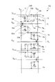
10a アクティブマトリクス基板
11 画素電極
12 走査線
13 信号線
13a 第1信号線
13b 第2信号線
14 薄膜トランジスタ(TFT)
15 補助容量配線
20 走査線駆動回路(ゲートドライバ)
30 信号線駆動回路(ソースドライバ)
100 液晶表示装置
P、P1、P2、P3、P4 画素
PCD カラー表示画素
Claims (8)
- 複数の行および複数の列を含むマトリクス状に配列された複数の画素を有する液晶表示装置であって、
前記複数の画素のそれぞれに設けられた画素電極、前記画素電極に接続されたスイッチング素子、行方向に延びる複数の走査線および列方向に延びる複数の信号線を有するアクティブマトリクス基板と、
前記アクティブマトリクス基板に対向する対向基板と、
前記アクティブマトリクス基板と前記対向基板との間に設けられた液晶層と、
前記複数の走査線のそれぞれに走査信号を供給する走査線駆動回路と、
前記複数の信号線のそれぞれに正または負の信号電圧を供給する信号線駆動回路と、
を備え、
前記複数の画素は、複数のカラー表示画素を構成しており、前記複数のカラー表示画素のそれぞれは、2行2列に配列された第1、第2、第3および第4画素であって、前記第1と第2画素および前記第3と第4画素がそれぞれ前記行方向に沿って隣接し、且つ、前記第1と第3画素および前記第2と第4画素がそれぞれ前記列方向に沿って隣接して配列された、第1、第2、第3および第4画素を含み、
前記第1、第2、第3および第4画素の色は、互いに異なり、前記複数のカラー表示画素のそれぞれにおいて、前記第1、第2、第3および第4画素は、同じパターンで配列され、
前記複数の信号線は、各画素列に対応して配置された第1および第2信号線であって、各垂直走査期間において、前記信号線駆動回路から互いに逆の極性の信号電圧が供給される第1信号線および第2信号線を含み、
任意のカラー表示画素において、前記第1および第3画素の一方の前記スイッチング素子は前記第1信号線に接続されており、他方の前記スイッチング素子は前記第2信号線に接続されており、前記第2および第4画素の一方の前記スイッチング素子は前記第1信号線に接続されており、他方のスイッチング素子は前記第2信号線に接続されており、かつ、前記第1、第2、第3および第4画素のスイッチング素子は全て、共通の走査信号によってオン/オフ制御され、
任意の垂直走査期間において、前記第1および第2信号線に供給される前記信号電圧の極性は一定であり、
任意の垂直走査期間において、任意のカラー表示画素に含まれる前記第1、第2、第3および第4画素のそれぞれに供給される前記信号電圧の極性と、前記任意のカラー表示画素に行方向に隣接するカラー表示画素に含まれる前記第1、第2、第3および第4画素のそれぞれに供給される前記信号電圧の極性とは、互いに逆である、液晶表示装置。 - 前記任意のカラー表示画素に列方向に隣接するカラー表示画素において、前記第1および第3画素の前記一方の前記スイッチング素子は前記第2信号線に接続されており、前記他方の前記スイッチング素子は前記第1信号線に接続されており、前記第2および第4画素の前記一方の前記スイッチング素子は前記第2信号線に接続されており、前記他方のスイッチング素子は前記第1信号線に接続されている、請求項1に記載の液晶表示装置。
- 任意の垂直走査期間において、任意の第1カラー表示画素に含まれる前記第1、第2、第3および第4画素のそれぞれに供給される前記信号電圧の極性は、前記第1画素と第2画素との間および前記第3画素と第4画素との間で互いに逆になる、請求項1または2に記載の液晶表示装置。
- 任意の垂直走査期間において、前記複数の信号線の内の互いに隣接する任意の2本の信号線に供給される前記信号電圧の極性は互いに逆である、請求項1から3のいずれかに記載の液晶表示装置。
- 任意のカラー表示画素において、前記第1、第2、第3および第4画素のスイッチング素子は全て、共通の走査線に接続されている、請求項1から4のいずれかに記載の液晶表示装置。
- 前記第1、第2、第3および第4画素は、黄画素、シアン画素、マゼンタ画素および白画素のいずれか1つと、赤画素、青画素および緑画素とを含む、請求項1から5のいずれかに記載の液晶表示装置。
- 前記複数の画素のそれぞれは、ある中間調を表示するときに、表示すべき中間調よりも高い輝度を呈する明副画素と、表示すべき中間調よりも低い輝度を呈する暗副画素とを有する、請求項1から6のいずれかに記載の液晶表示装置。
- 垂直走査期間は1/120秒以下である、請求項1から7のいずれかに記載の液晶表示装置。
Priority Applications (1)
| Application Number | Priority Date | Filing Date | Title |
|---|---|---|---|
| JP2011551896A JP5540020B2 (ja) | 2010-01-29 | 2011-01-27 | 液晶表示装置 |
Applications Claiming Priority (4)
| Application Number | Priority Date | Filing Date | Title |
|---|---|---|---|
| JP2010019258 | 2010-01-29 | ||
| JP2010019258 | 2010-01-29 | ||
| JP2011551896A JP5540020B2 (ja) | 2010-01-29 | 2011-01-27 | 液晶表示装置 |
| PCT/JP2011/051586 WO2011093374A1 (ja) | 2010-01-29 | 2011-01-27 | 液晶表示装置 |
Publications (2)
| Publication Number | Publication Date |
|---|---|
| JPWO2011093374A1 JPWO2011093374A1 (ja) | 2013-06-06 |
| JP5540020B2 true JP5540020B2 (ja) | 2014-07-02 |
Family
ID=44319357
Family Applications (1)
| Application Number | Title | Priority Date | Filing Date |
|---|---|---|---|
| JP2011551896A Expired - Fee Related JP5540020B2 (ja) | 2010-01-29 | 2011-01-27 | 液晶表示装置 |
Country Status (5)
| Country | Link |
|---|---|
| US (1) | US9818348B2 (ja) |
| EP (1) | EP2530513A4 (ja) |
| JP (1) | JP5540020B2 (ja) |
| CN (1) | CN102725676B (ja) |
| WO (1) | WO2011093374A1 (ja) |
Families Citing this family (16)
| Publication number | Priority date | Publication date | Assignee | Title |
|---|---|---|---|---|
| CN102750919A (zh) * | 2012-06-26 | 2012-10-24 | 北京京东方光电科技有限公司 | 一种显示面板及其驱动方法、显示装置 |
| CN104620309B (zh) * | 2012-09-13 | 2017-09-22 | 夏普株式会社 | 液晶显示装置 |
| WO2014087781A1 (ja) * | 2012-12-07 | 2014-06-12 | 堺ディスプレイプロダクト株式会社 | 液晶表示装置及び該液晶表示装置の駆動方法 |
| KR102114818B1 (ko) * | 2013-09-09 | 2020-05-26 | 삼성디스플레이 주식회사 | 표시 장치 |
| US9697787B2 (en) * | 2013-09-09 | 2017-07-04 | Samsung Display Co., Ltd. | Display device |
| CN103792746A (zh) | 2014-01-27 | 2014-05-14 | 北京京东方光电科技有限公司 | 一种阵列基板、其制备方法及显示装置 |
| JP2015165272A (ja) | 2014-03-03 | 2015-09-17 | 株式会社ジャパンディスプレイ | 表示装置及び反射型液晶表示装置 |
| KR20160025146A (ko) * | 2014-08-26 | 2016-03-08 | 삼성디스플레이 주식회사 | 표시 장치 |
| JP2016184097A (ja) | 2015-03-26 | 2016-10-20 | 株式会社ジャパンディスプレイ | 表示装置 |
| CN107924662A (zh) | 2015-08-27 | 2018-04-17 | 堺显示器制品株式会社 | 液晶显示装置 |
| CN105954951B (zh) * | 2016-07-08 | 2019-03-22 | 深圳市华星光电技术有限公司 | 一种液晶显示面板 |
| JP7021407B2 (ja) | 2017-07-11 | 2022-02-17 | トライベイル テクノロジーズ, エルエルシー | 表示装置、及び、その駆動方法 |
| JP2019049590A (ja) | 2017-09-08 | 2019-03-28 | シャープ株式会社 | アクティブマトリクス基板およびデマルチプレクサ回路 |
| CN107871485B (zh) * | 2017-12-19 | 2019-08-27 | 惠科股份有限公司 | 一种显示面板、显示装置及驱动方法 |
| JP2022178523A (ja) | 2021-05-20 | 2022-12-02 | シャープディスプレイテクノロジー株式会社 | アクティブマトリクス基板および液晶表示装置 |
| CN113325644A (zh) * | 2021-05-31 | 2021-08-31 | Tcl华星光电技术有限公司 | 显示面板和电子设备 |
Citations (3)
| Publication number | Priority date | Publication date | Assignee | Title |
|---|---|---|---|---|
| JP2001033757A (ja) * | 1999-07-21 | 2001-02-09 | Nec Corp | アクティブマトリクス型液晶表示装置 |
| WO2009084331A1 (ja) * | 2007-12-27 | 2009-07-09 | Sharp Kabushiki Kaisha | 液晶表示装置、液晶表示装置の駆動方法、テレビジョン受像機 |
| JP2009175468A (ja) * | 2008-01-25 | 2009-08-06 | Hitachi Displays Ltd | 表示装置 |
Family Cites Families (16)
| Publication number | Priority date | Publication date | Assignee | Title |
|---|---|---|---|---|
| JP2001272697A (ja) * | 2000-03-23 | 2001-10-05 | Hitachi Ltd | 液晶表示装置 |
| US6977704B2 (en) | 2001-03-30 | 2005-12-20 | Fujitsu Display Technologies Corporation | Liquid crystal display |
| JP4237977B2 (ja) | 2001-10-02 | 2009-03-11 | シャープ株式会社 | 液晶表示装置 |
| US6952252B2 (en) | 2001-10-02 | 2005-10-04 | Fujitsu Display Technologies Corporation | Substrate for liquid crystal display and liquid crystal display utilizing the same |
| JP4031291B2 (ja) * | 2001-11-14 | 2008-01-09 | 東芝松下ディスプレイテクノロジー株式会社 | 液晶表示装置 |
| JP3999081B2 (ja) * | 2002-01-30 | 2007-10-31 | シャープ株式会社 | 液晶表示装置 |
| JP4342200B2 (ja) | 2002-06-06 | 2009-10-14 | シャープ株式会社 | 液晶表示装置 |
| JP4372648B2 (ja) | 2004-09-13 | 2009-11-25 | シャープ株式会社 | 液晶表示装置およびその製造方法 |
| JP4571845B2 (ja) | 2004-11-08 | 2010-10-27 | シャープ株式会社 | 液晶表示装置用基板及びそれを備えた液晶表示装置及びその駆動方法 |
| JP2008076416A (ja) * | 2004-12-27 | 2008-04-03 | Sharp Corp | 表示パネルの駆動装置、表示パネル及びそれを備えた表示装置並びに表示パネルの駆動方法 |
| CN101317212B (zh) * | 2005-11-30 | 2012-07-04 | 夏普株式会社 | 用于驱动显示元件的显示设备和方法 |
| KR101359918B1 (ko) | 2006-09-26 | 2014-02-07 | 삼성디스플레이 주식회사 | 액정 표시 장치 |
| WO2008047725A1 (en) * | 2006-10-13 | 2008-04-24 | Sharp Kabushiki Kaisha | Display device, and signal converting device |
| JP5376723B2 (ja) * | 2008-06-09 | 2013-12-25 | 株式会社半導体エネルギー研究所 | 液晶表示装置 |
| US20100020257A1 (en) * | 2008-07-23 | 2010-01-28 | Samsung Electronics Co., Ltd. | Liquid crystal display device and manufacturing method thereof |
| CN101424821B (zh) | 2008-12-09 | 2012-10-31 | 友达光电股份有限公司 | 像素结构 |
-
2011
- 2011-01-27 JP JP2011551896A patent/JP5540020B2/ja not_active Expired - Fee Related
- 2011-01-27 CN CN201180007473.9A patent/CN102725676B/zh not_active Expired - Fee Related
- 2011-01-27 US US13/575,691 patent/US9818348B2/en not_active Expired - Fee Related
- 2011-01-27 WO PCT/JP2011/051586 patent/WO2011093374A1/ja not_active Ceased
- 2011-01-27 EP EP11737085.8A patent/EP2530513A4/en not_active Withdrawn
Patent Citations (3)
| Publication number | Priority date | Publication date | Assignee | Title |
|---|---|---|---|---|
| JP2001033757A (ja) * | 1999-07-21 | 2001-02-09 | Nec Corp | アクティブマトリクス型液晶表示装置 |
| WO2009084331A1 (ja) * | 2007-12-27 | 2009-07-09 | Sharp Kabushiki Kaisha | 液晶表示装置、液晶表示装置の駆動方法、テレビジョン受像機 |
| JP2009175468A (ja) * | 2008-01-25 | 2009-08-06 | Hitachi Displays Ltd | 表示装置 |
Also Published As
| Publication number | Publication date |
|---|---|
| CN102725676A (zh) | 2012-10-10 |
| CN102725676B (zh) | 2015-10-07 |
| JPWO2011093374A1 (ja) | 2013-06-06 |
| US9818348B2 (en) | 2017-11-14 |
| US20120320026A1 (en) | 2012-12-20 |
| WO2011093374A1 (ja) | 2011-08-04 |
| EP2530513A1 (en) | 2012-12-05 |
| EP2530513A4 (en) | 2013-08-14 |
Similar Documents
| Publication | Publication Date | Title |
|---|---|---|
| JP5540020B2 (ja) | 液晶表示装置 | |
| CN102725681B (zh) | 液晶显示装置 | |
| US8654050B2 (en) | Multiple-primary-color liquid crystal display device | |
| KR100711230B1 (ko) | 액정표시장치 | |
| EP2541310B1 (en) | Liquid crystal display device | |
| US8885131B2 (en) | Liquid crystal display device | |
| JPWO2011049106A1 (ja) | 液晶表示装置 | |
| US8319918B2 (en) | Multi-domain display using fringe fields | |
| CN109164611B (zh) | 阵列基板及其驱动方法和液晶显示装置及其驱动方法 | |
| US8467019B2 (en) | Low cost switching element point inversion driving scheme for liquid crystal displays | |
| US7999900B2 (en) | Display unit with interleaved pixels | |
| US7956958B2 (en) | Large-pixel multi-domain vertical alignment liquid crystal display using fringe fields | |
| US20120154716A1 (en) | Liquid crystal display | |
| US8605239B2 (en) | Display unit with interleaved pixels | |
| JP2008158286A (ja) | 液晶表示装置 | |
| KR20120008381A (ko) | 액정 표시 장치 | |
| WO2011105503A1 (ja) | 液晶表示装置 | |
| WO2011081160A1 (ja) | 液晶表示装置 | |
| KR20120044777A (ko) | 액정 표시 장치 |
Legal Events
| Date | Code | Title | Description |
|---|---|---|---|
| A131 | Notification of reasons for refusal |
Free format text: JAPANESE INTERMEDIATE CODE: A131 Effective date: 20140121 |
|
| A521 | Request for written amendment filed |
Free format text: JAPANESE INTERMEDIATE CODE: A523 Effective date: 20140318 |
|
| TRDD | Decision of grant or rejection written | ||
| A01 | Written decision to grant a patent or to grant a registration (utility model) |
Free format text: JAPANESE INTERMEDIATE CODE: A01 Effective date: 20140408 |
|
| R150 | Certificate of patent or registration of utility model |
Ref document number: 5540020 Country of ref document: JP Free format text: JAPANESE INTERMEDIATE CODE: R150 |
|
| A61 | First payment of annual fees (during grant procedure) |
Free format text: JAPANESE INTERMEDIATE CODE: A61 Effective date: 20140501 |
|
| LAPS | Cancellation because of no payment of annual fees |