JP5543383B2 - 埋め込み絶縁層を貫いて半導体層間に接触を有するデバイス、およびこのデバイスの製造プロセス - Google Patents
埋め込み絶縁層を貫いて半導体層間に接触を有するデバイス、およびこのデバイスの製造プロセス Download PDFInfo
- Publication number
- JP5543383B2 JP5543383B2 JP2011004142A JP2011004142A JP5543383B2 JP 5543383 B2 JP5543383 B2 JP 5543383B2 JP 2011004142 A JP2011004142 A JP 2011004142A JP 2011004142 A JP2011004142 A JP 2011004142A JP 5543383 B2 JP5543383 B2 JP 5543383B2
- Authority
- JP
- Japan
- Prior art keywords
- region
- conductive
- semiconductor
- insulating layer
- thin layer
- Prior art date
- Legal status (The legal status is an assumption and is not a legal conclusion. Google has not performed a legal analysis and makes no representation as to the accuracy of the status listed.)
- Active
Links
Images






Classifications
-
- H—ELECTRICITY
- H10—SEMICONDUCTOR DEVICES; ELECTRIC SOLID-STATE DEVICES NOT OTHERWISE PROVIDED FOR
- H10D—INORGANIC ELECTRIC SEMICONDUCTOR DEVICES
- H10D48/00—Individual devices not covered by groups H10D1/00 - H10D44/00
- H10D48/30—Devices controlled by electric currents or voltages
- H10D48/32—Devices controlled by only the electric current supplied, or only the electric potential applied, to an electrode which does not carry the current to be rectified, amplified or switched
- H10D48/34—Bipolar devices
-
- H—ELECTRICITY
- H10—SEMICONDUCTOR DEVICES; ELECTRIC SOLID-STATE DEVICES NOT OTHERWISE PROVIDED FOR
- H10D—INORGANIC ELECTRIC SEMICONDUCTOR DEVICES
- H10D86/00—Integrated devices formed in or on insulating or conducting substrates, e.g. formed in silicon-on-insulator [SOI] substrates or on stainless steel or glass substrates
- H10D86/201—Integrated devices formed in or on insulating or conducting substrates, e.g. formed in silicon-on-insulator [SOI] substrates or on stainless steel or glass substrates the substrates comprising an insulating layer on a semiconductor body, e.g. SOI
-
- H—ELECTRICITY
- H10—SEMICONDUCTOR DEVICES; ELECTRIC SOLID-STATE DEVICES NOT OTHERWISE PROVIDED FOR
- H10B—ELECTRONIC MEMORY DEVICES
- H10B12/00—Dynamic random access memory [DRAM] devices
- H10B12/20—DRAM devices comprising floating-body transistors, e.g. floating-body cells
-
- H—ELECTRICITY
- H10—SEMICONDUCTOR DEVICES; ELECTRIC SOLID-STATE DEVICES NOT OTHERWISE PROVIDED FOR
- H10D—INORGANIC ELECTRIC SEMICONDUCTOR DEVICES
- H10D10/00—Bipolar junction transistors [BJT]
- H10D10/40—Vertical BJTs
-
- H—ELECTRICITY
- H10—SEMICONDUCTOR DEVICES; ELECTRIC SOLID-STATE DEVICES NOT OTHERWISE PROVIDED FOR
- H10D—INORGANIC ELECTRIC SEMICONDUCTOR DEVICES
- H10D8/00—Diodes
-
- H—ELECTRICITY
- H10—SEMICONDUCTOR DEVICES; ELECTRIC SOLID-STATE DEVICES NOT OTHERWISE PROVIDED FOR
- H10D—INORGANIC ELECTRIC SEMICONDUCTOR DEVICES
- H10D86/00—Integrated devices formed in or on insulating or conducting substrates, e.g. formed in silicon-on-insulator [SOI] substrates or on stainless steel or glass substrates
- H10D86/01—Manufacture or treatment
-
- H—ELECTRICITY
- H10—SEMICONDUCTOR DEVICES; ELECTRIC SOLID-STATE DEVICES NOT OTHERWISE PROVIDED FOR
- H10W—GENERIC PACKAGES, INTERCONNECTIONS, CONNECTORS OR OTHER CONSTRUCTIONAL DETAILS OF DEVICES COVERED BY CLASS H10
- H10W20/00—Interconnections in chips, wafers or substrates
- H10W20/01—Manufacture or treatment
- H10W20/021—Manufacture or treatment of interconnections within wafers or substrates
-
- H—ELECTRICITY
- H10—SEMICONDUCTOR DEVICES; ELECTRIC SOLID-STATE DEVICES NOT OTHERWISE PROVIDED FOR
- H10B—ELECTRONIC MEMORY DEVICES
- H10B12/00—Dynamic random access memory [DRAM] devices
- H10B12/01—Manufacture or treatment
- H10B12/02—Manufacture or treatment for one transistor one-capacitor [1T-1C] memory cells
- H10B12/05—Making the transistor
-
- H—ELECTRICITY
- H10—SEMICONDUCTOR DEVICES; ELECTRIC SOLID-STATE DEVICES NOT OTHERWISE PROVIDED FOR
- H10D—INORGANIC ELECTRIC SEMICONDUCTOR DEVICES
- H10D30/00—Field-effect transistors [FET]
- H10D30/60—Insulated-gate field-effect transistors [IGFET]
- H10D30/67—Thin-film transistors [TFT]
- H10D30/6704—Thin-film transistors [TFT] having supplementary regions or layers in the thin films or in the insulated bulk substrates for controlling properties of the device
- H10D30/6727—Thin-film transistors [TFT] having supplementary regions or layers in the thin films or in the insulated bulk substrates for controlling properties of the device having source or drain regions connected to bulk conducting substrates
-
- H—ELECTRICITY
- H10—SEMICONDUCTOR DEVICES; ELECTRIC SOLID-STATE DEVICES NOT OTHERWISE PROVIDED FOR
- H10D—INORGANIC ELECTRIC SEMICONDUCTOR DEVICES
- H10D30/00—Field-effect transistors [FET]
- H10D30/60—Insulated-gate field-effect transistors [IGFET]
- H10D30/711—Insulated-gate field-effect transistors [IGFET] having floating bodies
Landscapes
- Semiconductor Memories (AREA)
- Bipolar Transistors (AREA)
- Thin Film Transistor (AREA)
- Element Separation (AREA)
Description
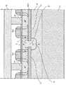
−第1の領域、第2の領域および接触は同じタイプの導電性を有する;
−第1の領域はトランジスタのドレイン領域で、第2の領域は埋め込みビットラインに属する;
−第1の領域はトランジスタのソース領域で、第2の領域は埋め込みソースラインに属する;
−第1の領域はバイポーラトランジスタのエミッターから成り、第2の領域は埋め込み注入ラインに属する;
−第2の領域はトランジスタのバックコントロールゲート領域であり、第1の領域はバックコントロールゲートドライブラインに属する;
−接触は金属相互接続材料により形成される;
−第1の領域および第2の領域は逆のタイプの導電性を有し、接触は、導電性が第1の領域と同じタイプの導電性である上部領域および導電性が第2の領域と同じタイプの導電性である下部領域を有する。
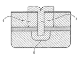
−接触を形成するために、以下のステップが実行される:
・埋め込み絶縁層を超えて、第1の領域を貫通し、第2の領域に到達するまで延びた溝を内部に形成するための半導体基板のエッチング;および
・溝の内部接続材料による充填;
−内部接続材料は半導体材料である;
−内部接続材料は予めドープされている;
−溝内に半導体材料をドープするステップを更に含む;
−溝の上部領域および下部領域は正負逆にドープされている;
−上部領域と下部領域との境界は絶縁層と水平に位置している;
−上部領域と下部領域との境界は第1の領域上の薄い層と水平に位置している;
−内部接続材料は金属である。
Claims (14)
- 半導体材料の薄い層と、
ベース基板と、
前記薄い層と前記ベース基板とを隔離する埋め込み絶縁層と、
を含み、前記薄い層は電界効果トランジスタのソース領域及びチャネル領域を含み、前記ベース基板は埋め込み注入ラインを含む、SeOI(Semiconductor−On−Insulator)基板上に作製された半導体デバイスであって、前記半導体デバイスは、
前記薄い層内の第1の伝導領域と、
前記ベース基板内の第2の伝導領域であって、前記第2の伝導領域は前記埋め込み注入ラインに含まれる、第2の伝導領域と、
前記埋め込み絶縁層を貫通して前記第1の伝導領域と前記第2の伝導領域とを接続する接触部と、を含み、
前記第1の伝導領域は、バイポーラトランジスタのエミッター、前記電界効果トランジスタの前記ソース領域によって形成される前記バイポーラトランジスタのベースおよび前記電界効果トランジスタの前記チャネル領域によって形成される前記バイポーラトランジスタのコレクタを構成することを特徴とする半導体デバイス。 - 前記第2の伝導領域はバックコントロールゲート領域であり、前記第1の伝導領域はバックコントロールゲートドライブラインに属することを特徴とする請求項1に記載の半導体デバイス。
- 前記接触部はドープされた半導体内部接続材料によって形成されることを特徴とする請求項1または2に記載の半導体デバイス。
- 前記接触部は、前記第1の伝導領域と同じ型の導電性である下部領域と、逆の型の導電性である上部領域とを有することを特徴とする請求項1乃至3のいずれか1項に記載の半導体デバイス。
- 前記上部領域と前記下部領域との境界は前記埋め込み絶縁層と同じ水平面上に位置することを特徴とする請求項4に記載の半導体デバイス。
- 前記上部領域と前記下部領域との境界は前記第1の伝導領域上の前記薄い層と同じ水平面上に位置することを特徴とする請求項4に記載の半導体デバイス。
- 半導体材料の薄い層と、
ベース基板と、
前記薄い層と前記ベース基板との間に埋め込まれ、前記薄い層と前記ベース基板とを隔離する埋め込み絶縁層と、
を含み、前記薄い層は電界効果トランジスタのソース領域及びチャネル領域を含み、前記ベース基板は埋め込み注入ラインを含む、SeOI(Semiconductor−On−Insulator)基板上に作製された半導体デバイスを製作するプロセスであって、前記半導体デバイスは、
前記薄い層内の第1の伝導領域と、
前記ベース基板内の第2の伝導領域であって、前記第2の伝導領域は前記埋め込み注入ライン内に含まれる、第2の伝導領域と、を含み、
前記第1の伝導領域は、バイポーラトランジスタのエミッター、前記電界効果トランジスタの前記ソース領域によって形成される前記バイポーラトランジスタのベースおよび前記電界効果トランジスタの前記チャネル領域によって形成される前記バイポーラトランジスタのコレクタを構成し、
前記プロセスは、前記埋め込み絶縁層を貫通して前記第1の伝導領域と前記第2の伝導領域を接続する接触部を形成するステップを含むことを特徴とするプロセス。 - 前記接触部を形成するために、
前記半導体基板内に、前記埋め込み絶縁層を越えて、前記第1の伝導領域を貫通し、前記第2の伝導領域に到達するまで延びている溝(6)を形成するために前記半導体基板をエッチングするステップと、
内部接続材料によって前記溝を充填するステップと
が実行されることを特徴とする請求項7に記載のプロセス。 - 前記内部接続材料は事前にドープされた半導体材料であることを特徴とする請求項8に記載のプロセス。
- 前記内部接続材料は半導体材料であり、前記溝内の前記半導体材料にドーピングするステップを更に含むことを特徴とする請求項9に記載のプロセス。
- 前記溝内の前記半導体材料にドーピングするステップは、前記溝内にドーパントを拡散させるアニーリング工程によって実行されることを特徴とする請求項10に記載のプロセス。
- 前記溝の上部領域(8)と下部領域(9)が逆の型の導電性を有することを特徴とする請求項9乃至11のいずれか1項に記載のプロセス。
- 前記上部領域と前記下部領域との境界は前記埋め込み絶縁層と同じ水平面上に位置することを特徴とする請求項12に記載のプロセス。
- 前記上部領域と前記下部領域との境界は前記第1の伝導領域上の前記薄い層と同じ水平面上に位置することを特徴とする請求項12に記載のプロセス。
Applications Claiming Priority (2)
| Application Number | Priority Date | Filing Date | Title |
|---|---|---|---|
| FR1050244 | 2010-01-14 | ||
| FR1050244A FR2955200B1 (fr) | 2010-01-14 | 2010-01-14 | Dispositif, et son procede de fabrication, disposant d'un contact entre regions semi-conductrices a travers une couche isolante enterree |
Publications (2)
| Publication Number | Publication Date |
|---|---|
| JP2011155259A JP2011155259A (ja) | 2011-08-11 |
| JP5543383B2 true JP5543383B2 (ja) | 2014-07-09 |
Family
ID=42342015
Family Applications (1)
| Application Number | Title | Priority Date | Filing Date |
|---|---|---|---|
| JP2011004142A Active JP5543383B2 (ja) | 2010-01-14 | 2011-01-12 | 埋め込み絶縁層を貫いて半導体層間に接触を有するデバイス、およびこのデバイスの製造プロセス |
Country Status (8)
| Country | Link |
|---|---|
| US (1) | US9490264B2 (ja) |
| EP (1) | EP2355143A1 (ja) |
| JP (1) | JP5543383B2 (ja) |
| KR (1) | KR101277328B1 (ja) |
| CN (1) | CN102184927B (ja) |
| FR (1) | FR2955200B1 (ja) |
| SG (1) | SG173270A1 (ja) |
| TW (1) | TWI455270B (ja) |
Families Citing this family (7)
| Publication number | Priority date | Publication date | Assignee | Title |
|---|---|---|---|---|
| US9768254B2 (en) * | 2015-07-30 | 2017-09-19 | International Business Machines Corporation | Leakage-free implantation-free ETSOI transistors |
| DE102015015699A1 (de) | 2015-12-04 | 2017-06-08 | Abb Schweiz Ag | Elektronisches Leistungsmodul |
| FR3095891B1 (fr) * | 2019-05-09 | 2023-01-13 | St Microelectronics Sa | Circuit électronique |
| KR102690949B1 (ko) | 2019-06-14 | 2024-08-02 | 에스케이하이닉스 주식회사 | 반도체 장치 및 그 제조 방법 |
| WO2021242721A1 (en) * | 2020-05-28 | 2021-12-02 | Zeno Semiconductor, Inc. | A memory device comprising an electrically floating body transistor |
| US11894450B2 (en) * | 2021-11-18 | 2024-02-06 | Globalfoundries U.S. Inc. | Lateral bipolar transistor with emitter and collector regions including portions within In-insulator layer cavities and method |
| KR20230165567A (ko) | 2022-05-27 | 2023-12-05 | 삼성전자주식회사 | 반도체 메모리 소자 및 그 제조방법 |
Family Cites Families (108)
| Publication number | Priority date | Publication date | Assignee | Title |
|---|---|---|---|---|
| US4169233A (en) | 1978-02-24 | 1979-09-25 | Rockwell International Corporation | High performance CMOS sense amplifier |
| KR100213602B1 (ko) | 1988-05-13 | 1999-08-02 | 가나이 쓰도무 | 다이나믹형 반도체 기억장치 |
| US5028810A (en) | 1989-07-13 | 1991-07-02 | Intel Corporation | Four quadrant synapse cell employing single column summing line |
| JPH0432446A (ja) * | 1990-05-25 | 1992-02-04 | Matsushita Graphic Commun Syst Inc | 情報通信装置 |
| JP3128829B2 (ja) | 1990-12-26 | 2001-01-29 | ソニー株式会社 | 半導体メモリ装置 |
| JP3003188B2 (ja) | 1990-09-10 | 2000-01-24 | ソニー株式会社 | 半導体メモリ及びその製造方法 |
| JPH04280469A (ja) | 1991-03-07 | 1992-10-06 | Mitsubishi Electric Corp | 半導体装置 |
| JPH04345064A (ja) | 1991-05-22 | 1992-12-01 | Hitachi Ltd | 半導体集積回路装置およびその製造方法 |
| JP2717740B2 (ja) | 1991-08-30 | 1998-02-25 | 三菱電機株式会社 | 半導体集積回路装置 |
| EP0836194B1 (en) | 1992-03-30 | 2000-05-24 | Mitsubishi Denki Kabushiki Kaisha | Semiconductor device |
| US5325054A (en) * | 1992-07-07 | 1994-06-28 | Texas Instruments Incorporated | Method and system for screening reliability of semiconductor circuits |
| US5306530A (en) * | 1992-11-23 | 1994-04-26 | Associated Universities, Inc. | Method for producing high quality thin layer films on substrates |
| JP3488730B2 (ja) | 1993-11-05 | 2004-01-19 | 株式会社ルネサステクノロジ | 半導体集積回路装置 |
| US5455791A (en) | 1994-06-01 | 1995-10-03 | Zaleski; Andrzei | Method for erasing data in EEPROM devices on SOI substrates and device therefor |
| JP3003088B2 (ja) * | 1994-06-10 | 2000-01-24 | 住友イートンノバ株式会社 | イオン注入装置 |
| JP3549602B2 (ja) | 1995-01-12 | 2004-08-04 | 株式会社ルネサステクノロジ | 半導体記憶装置 |
| JPH08255846A (ja) | 1995-03-17 | 1996-10-01 | Nippondenso Co Ltd | 半導体装置及びその製造方法 |
| JP3288554B2 (ja) * | 1995-05-29 | 2002-06-04 | 株式会社日立製作所 | イオン注入装置及びイオン注入方法 |
| JPH0982814A (ja) * | 1995-07-10 | 1997-03-28 | Denso Corp | 半導体集積回路装置及びその製造方法 |
| JPH0982918A (ja) * | 1995-09-19 | 1997-03-28 | Toshiba Corp | 半導体記憶装置およびその製造方法 |
| US6787844B2 (en) * | 1995-09-29 | 2004-09-07 | Nippon Steel Corporation | Semiconductor device including transistor with composite gate structure and transistor with single gate structure, and method for manufacturing the same |
| JP3265178B2 (ja) * | 1996-02-20 | 2002-03-11 | 株式会社東芝 | 半導体記憶装置及びその製造方法 |
| JP3489090B2 (ja) | 1996-02-27 | 2004-01-19 | 富士通株式会社 | 半導体装置及びその製造方法 |
| JPH10125064A (ja) | 1996-10-14 | 1998-05-15 | Toshiba Corp | 記憶装置 |
| US6121661A (en) * | 1996-12-11 | 2000-09-19 | International Business Machines Corporation | Silicon-on-insulator structure for electrostatic discharge protection and improved heat dissipation |
| JPH10208484A (ja) | 1997-01-29 | 1998-08-07 | Mitsubishi Electric Corp | 半導体記憶装置のデータ読出回路及び半導体記憶装置 |
| US5889293A (en) * | 1997-04-04 | 1999-03-30 | International Business Machines Corporation | Electrical contact to buried SOI structures |
| JP3699823B2 (ja) | 1998-05-19 | 2005-09-28 | 株式会社東芝 | 半導体装置 |
| US6072217A (en) | 1998-06-11 | 2000-06-06 | Sun Microsystems, Inc. | Tunable threshold SOI device using isolated well structure for back gate |
| FR2779869B1 (fr) | 1998-06-15 | 2003-05-16 | Commissariat Energie Atomique | Circuit integre de type soi a capacite de decouplage, et procede de realisation d'un tel circuit |
| US6826730B2 (en) | 1998-12-15 | 2004-11-30 | Texas Instruments Incorporated | System and method for controlling current in an integrated circuit |
| JP3456913B2 (ja) | 1998-12-25 | 2003-10-14 | 株式会社東芝 | 半導体装置 |
| KR100618789B1 (ko) | 1999-07-30 | 2006-09-06 | 삼성전자주식회사 | 소이 구조의 씨모스와 수직형 바이폴라 트랜지스터를 갖는 바이씨모스 |
| US6372600B1 (en) * | 1999-08-30 | 2002-04-16 | Agere Systems Guardian Corp. | Etch stops and alignment marks for bonded wafers |
| US6476462B2 (en) | 1999-12-28 | 2002-11-05 | Texas Instruments Incorporated | MOS-type semiconductor device and method for making same |
| US6417697B2 (en) | 2000-02-02 | 2002-07-09 | Broadcom Corporation | Circuit technique for high speed low power data transfer bus |
| US6300218B1 (en) | 2000-05-08 | 2001-10-09 | International Business Machines Corporation | Method for patterning a buried oxide thickness for a separation by implanted oxygen (simox) process |
| JP2002110990A (ja) * | 2000-09-27 | 2002-04-12 | Toshiba Corp | 半導体装置およびその製造方法 |
| US6350653B1 (en) | 2000-10-12 | 2002-02-26 | International Business Machines Corporation | Embedded DRAM on silicon-on-insulator substrate |
| JP2002164544A (ja) * | 2000-11-28 | 2002-06-07 | Sony Corp | 半導体装置 |
| US6614190B2 (en) * | 2001-01-31 | 2003-09-02 | Hitachi, Ltd. | Ion implanter |
| JP3982218B2 (ja) | 2001-02-07 | 2007-09-26 | ソニー株式会社 | 半導体装置およびその製造方法 |
| JP3884266B2 (ja) | 2001-02-19 | 2007-02-21 | 株式会社東芝 | 半導体メモリ装置及びその製造方法 |
| US6611023B1 (en) | 2001-05-01 | 2003-08-26 | Advanced Micro Devices, Inc. | Field effect transistor with self alligned double gate and method of forming same |
| US6759282B2 (en) * | 2001-06-12 | 2004-07-06 | International Business Machines Corporation | Method and structure for buried circuits and devices |
| US6498057B1 (en) * | 2002-03-07 | 2002-12-24 | International Business Machines Corporation | Method for implementing SOI transistor source connections using buried dual rail distribution |
| EP1357603A3 (en) | 2002-04-18 | 2004-01-14 | Innovative Silicon SA | Semiconductor device |
| JP3594140B2 (ja) * | 2002-06-26 | 2004-11-24 | 沖電気工業株式会社 | 半導体装置の製造方法 |
| US6838723B2 (en) | 2002-08-29 | 2005-01-04 | Micron Technology, Inc. | Merged MOS-bipolar capacitor memory cell |
| US6790713B1 (en) * | 2002-09-09 | 2004-09-14 | T-Ram, Inc. | Method for making an inlayed thyristor-based device |
| US7710771B2 (en) * | 2002-11-20 | 2010-05-04 | The Regents Of The University Of California | Method and apparatus for capacitorless double-gate storage |
| JP2004179506A (ja) * | 2002-11-28 | 2004-06-24 | Seiko Epson Corp | Soi構造を有する半導体基板及びその製造方法及び半導体装置 |
| US7030436B2 (en) | 2002-12-04 | 2006-04-18 | Micron Technology, Inc. | Embedded DRAM gain memory cell having MOS transistor body provided with a bi-polar transistor charge injecting means |
| JP2004303499A (ja) | 2003-03-31 | 2004-10-28 | Hitachi High-Technologies Corp | イオン注入装置およびイオン注入方法 |
| JP4077381B2 (ja) | 2003-08-29 | 2008-04-16 | 株式会社東芝 | 半導体集積回路装置 |
| US6965143B2 (en) | 2003-10-10 | 2005-11-15 | Advanced Micro Devices, Inc. | Recess channel flash architecture for reduced short channel effect |
| JP2005158952A (ja) | 2003-11-25 | 2005-06-16 | Toshiba Corp | 半導体装置及びその製造方法 |
| US7109532B1 (en) | 2003-12-23 | 2006-09-19 | Lee Zachary K | High Ion/Ioff SOI MOSFET using body voltage control |
| US20050255666A1 (en) * | 2004-05-11 | 2005-11-17 | Miradia Inc. | Method and structure for aligning mechanical based device to integrated circuits |
| US7112997B1 (en) * | 2004-05-19 | 2006-09-26 | Altera Corporation | Apparatus and methods for multi-gate silicon-on-insulator transistors |
| JP4795653B2 (ja) | 2004-06-15 | 2011-10-19 | ルネサスエレクトロニクス株式会社 | 半導体記憶装置 |
| US7196921B2 (en) | 2004-07-19 | 2007-03-27 | Silicon Storage Technology, Inc. | High-speed and low-power differential non-volatile content addressable memory cell and array |
| US7190616B2 (en) | 2004-07-19 | 2007-03-13 | Micron Technology, Inc. | In-service reconfigurable DRAM and flash memory device |
| US7560361B2 (en) | 2004-08-12 | 2009-07-14 | International Business Machines Corporation | Method of forming gate stack for semiconductor electronic device |
| KR100663359B1 (ko) | 2005-03-31 | 2007-01-02 | 삼성전자주식회사 | 리세스 채널 트랜지스터 구조를 갖는 단일 트랜지스터플로팅 바디 디램 셀 및 그 제조방법 |
| US20060267064A1 (en) | 2005-05-31 | 2006-11-30 | Infineon Technologies Ag | Semiconductor memory device |
| US7274618B2 (en) * | 2005-06-24 | 2007-09-25 | Monolithic System Technology, Inc. | Word line driver for DRAM embedded in a logic process |
| JP4967264B2 (ja) | 2005-07-11 | 2012-07-04 | 株式会社日立製作所 | 半導体装置 |
| JP4800700B2 (ja) | 2005-08-01 | 2011-10-26 | ルネサスエレクトロニクス株式会社 | 半導体装置およびそれを用いた半導体集積回路 |
| US7314794B2 (en) * | 2005-08-08 | 2008-01-01 | International Business Machines Corporation | Low-cost high-performance planar back-gate CMOS |
| JP4413841B2 (ja) | 2005-10-03 | 2010-02-10 | 株式会社東芝 | 半導体記憶装置及びその製造方法 |
| JP4822791B2 (ja) | 2005-10-04 | 2011-11-24 | ルネサスエレクトロニクス株式会社 | 半導体記憶装置 |
| US7601271B2 (en) | 2005-11-28 | 2009-10-13 | S.O.I.Tec Silicon On Insulator Technologies | Process and equipment for bonding by molecular adhesion |
| JP5054919B2 (ja) | 2005-12-20 | 2012-10-24 | ルネサスエレクトロニクス株式会社 | 半導体集積回路装置 |
| KR100735613B1 (ko) * | 2006-01-11 | 2007-07-04 | 삼성전자주식회사 | 이온주입설비의 디스크 어셈블리 |
| US7304903B2 (en) | 2006-01-23 | 2007-12-04 | Purdue Research Foundation | Sense amplifier circuit |
| JP4762036B2 (ja) | 2006-04-14 | 2011-08-31 | 株式会社東芝 | 半導体装置 |
| US20090096936A1 (en) * | 2006-04-24 | 2009-04-16 | Panasonic Corporation | Receiving device, electronic device using the same, and receiving method |
| US7494902B2 (en) * | 2006-06-23 | 2009-02-24 | Interuniversitair Microelektronica Centrum Vzw (Imec) | Method of fabricating a strained multi-gate transistor |
| KR100843055B1 (ko) * | 2006-08-17 | 2008-07-01 | 주식회사 하이닉스반도체 | 플래쉬 메모리 소자 및 그의 제조방법 |
| US7560344B2 (en) | 2006-11-15 | 2009-07-14 | Samsung Electronics Co., Ltd. | Semiconductor device having a pair of fins and method of manufacturing the same |
| JP2008130670A (ja) * | 2006-11-17 | 2008-06-05 | Seiko Epson Corp | 半導体装置、論理回路および電子機器 |
| JP5057430B2 (ja) * | 2006-12-18 | 2012-10-24 | ルネサスエレクトロニクス株式会社 | 半導体集積回路とその製造方法 |
| JP4869088B2 (ja) | 2007-01-22 | 2012-02-01 | 株式会社東芝 | 半導体記憶装置及びその書き込み方法 |
| JP5019436B2 (ja) | 2007-02-22 | 2012-09-05 | ルネサスエレクトロニクス株式会社 | 半導体集積回路 |
| JP5594927B2 (ja) | 2007-04-11 | 2014-09-24 | ピーエスフォー ルクスコ エスエイアールエル | 半導体記憶装置 |
| FR2915024A1 (fr) | 2007-04-12 | 2008-10-17 | St Microelectronics Crolles 2 | Procede de fabrication permettant l'homogeneisation de l'environnement de transistors et dispositif associe |
| US7729149B2 (en) | 2007-05-01 | 2010-06-01 | Suvolta, Inc. | Content addressable memory cell including a junction field effect transistor |
| EP2015362A1 (en) | 2007-06-04 | 2009-01-14 | STMicroelectronics (Crolles 2) SAS | Semiconductor array and manufacturing method thereof |
| US7449922B1 (en) | 2007-06-15 | 2008-11-11 | Arm Limited | Sensing circuitry and method of detecting a change in voltage on at least one input line |
| US7759714B2 (en) | 2007-06-26 | 2010-07-20 | Hitachi, Ltd. | Semiconductor device |
| FR2918823B1 (fr) | 2007-07-13 | 2009-10-16 | Ecole Centrale De Lyon Etablis | Cellule logique reconfigurable a base de transistors mosfet double grille |
| FR2919112A1 (fr) * | 2007-07-16 | 2009-01-23 | St Microelectronics Crolles 2 | Circuit integre comprenant un transistor et un condensateur et procede de fabrication |
| JP5035345B2 (ja) | 2007-08-30 | 2012-09-26 | 富士通セミコンダクター株式会社 | イオン注入装置、基板クランプ機構、及びイオン注入方法 |
| KR100884344B1 (ko) | 2007-10-10 | 2009-02-18 | 주식회사 하이닉스반도체 | 비대칭 소스/드레인 접합을 갖는 불휘발성 메모리소자 및그 제조방법 |
| JP5222520B2 (ja) * | 2007-10-11 | 2013-06-26 | ルネサスエレクトロニクス株式会社 | 半導体装置の製造方法 |
| US20090101940A1 (en) | 2007-10-19 | 2009-04-23 | Barrows Corey K | Dual gate fet structures for flexible gate array design methodologies |
| DE102007052097B4 (de) * | 2007-10-31 | 2010-10-28 | Advanced Micro Devices, Inc., Sunnyvale | Verfahren zur Herstellung eines SOI-Bauelements mit einer Substratdiode |
| FR2925223B1 (fr) | 2007-12-18 | 2010-02-19 | Soitec Silicon On Insulator | Procede d'assemblage avec marques enterrees |
| US7593265B2 (en) | 2007-12-28 | 2009-09-22 | Sandisk Corporation | Low noise sense amplifier array and method for nonvolatile memory |
| WO2009104060A1 (en) | 2008-02-20 | 2009-08-27 | S.O.I.Tec Silicon On Insulator Technologies | Oxidation after oxide dissolution |
| JP6053250B2 (ja) | 2008-06-12 | 2016-12-27 | ピーエスフォー ルクスコ エスエイアールエルPS4 Luxco S.a.r.l. | 半導体装置 |
| WO2010007478A1 (en) | 2008-06-13 | 2010-01-21 | Yale University | Improved complementary metal oxide semiconductor devices |
| US8120110B2 (en) * | 2008-08-08 | 2012-02-21 | International Business Machines Corporation | Semiconductor structure including a high performance FET and a high voltage FET on a SOI substrate |
| US8012814B2 (en) * | 2008-08-08 | 2011-09-06 | International Business Machines Corporation | Method of forming a high performance fet and a high voltage fet on a SOI substrate |
| KR101623958B1 (ko) | 2008-10-01 | 2016-05-25 | 삼성전자주식회사 | 인버터 및 그의 동작방법과 인버터를 포함하는 논리회로 |
| KR101522400B1 (ko) | 2008-11-10 | 2015-05-21 | 삼성전자주식회사 | 인버터 및 그를 포함하는 논리소자 |
| FR2955204B1 (fr) * | 2010-01-14 | 2012-07-20 | Soitec Silicon On Insulator | Cellule memoire dram disposant d'un injecteur bipolaire vertical |
-
2010
- 2010-01-14 FR FR1050244A patent/FR2955200B1/fr active Active
-
2011
- 2011-01-04 US US12/984,466 patent/US9490264B2/en active Active
- 2011-01-12 TW TW100101081A patent/TWI455270B/zh active
- 2011-01-12 JP JP2011004142A patent/JP5543383B2/ja active Active
- 2011-01-12 CN CN201110038036.5A patent/CN102184927B/zh active Active
- 2011-01-12 KR KR1020110003089A patent/KR101277328B1/ko active Active
- 2011-01-13 EP EP11150845A patent/EP2355143A1/en not_active Withdrawn
- 2011-01-13 SG SG2011002458A patent/SG173270A1/en unknown
Also Published As
| Publication number | Publication date |
|---|---|
| FR2955200A1 (fr) | 2011-07-15 |
| CN102184927A (zh) | 2011-09-14 |
| JP2011155259A (ja) | 2011-08-11 |
| US20110169090A1 (en) | 2011-07-14 |
| FR2955200B1 (fr) | 2012-07-20 |
| EP2355143A1 (en) | 2011-08-10 |
| KR20110083540A (ko) | 2011-07-20 |
| TWI455270B (zh) | 2014-10-01 |
| TW201135894A (en) | 2011-10-16 |
| SG173270A1 (en) | 2011-08-29 |
| KR101277328B1 (ko) | 2013-06-20 |
| CN102184927B (zh) | 2014-11-05 |
| US9490264B2 (en) | 2016-11-08 |
Similar Documents
| Publication | Publication Date | Title |
|---|---|---|
| JP7273183B2 (ja) | 3次元メモリデバイスを形成するための方法 | |
| JP7532534B2 (ja) | バックサイドソースコンタクトを備える3次元メモリデバイスを形成するための方法 | |
| TWI898980B (zh) | 半導體裝置結構 | |
| US8987799B2 (en) | Semiconductor device and method of forming the same | |
| US8648414B2 (en) | Semiconductor structures including bodies of semiconductor material, devices including such structures and related methods | |
| US8263460B2 (en) | Method for manufacturing semiconductor device with buried gates | |
| JP2022538954A (ja) | 3次元メモリデバイス及び方法 | |
| CN111542924B (zh) | 集成组合件及形成集成组合件的方法 | |
| JP5543383B2 (ja) | 埋め込み絶縁層を貫いて半導体層間に接触を有するデバイス、およびこのデバイスの製造プロセス | |
| KR20110099502A (ko) | 반도체 소자 및 그 제조 방법 | |
| CN115915751B (zh) | 半导体结构的制备方法 | |
| JP5102767B2 (ja) | サイド・ゲート及びトップ・ゲート読み出しトランジスタを有するデュアル・ポート型ゲインセル | |
| TW201017814A (en) | Semiconductor device and method of manufacturing the same | |
| KR20230128963A (ko) | Bspdn 구조물을 갖는 반도체 장치의 pn 접합 소자 구조 | |
| CN114334969A (zh) | 半导体结构及半导体结构的制作方法 | |
| TWI779318B (zh) | 三維記憶體元件及其製作方法 | |
| US7714388B2 (en) | Semiconductor memory device and manufacturing method thereof | |
| WO2023137800A1 (zh) | 半导体结构及其制造方法 | |
| JP2010232361A (ja) | 半導体記憶装置 | |
| CN113990800A (zh) | 半导体器件的制备方法及半导体器件 | |
| CN116266575B (zh) | 存储器元件及其制备方法 | |
| WO2022033164A1 (zh) | 半导体结构及半导体结构的制造方法 |
Legal Events
| Date | Code | Title | Description |
|---|---|---|---|
| A621 | Written request for application examination |
Free format text: JAPANESE INTERMEDIATE CODE: A621 Effective date: 20110314 |
|
| A131 | Notification of reasons for refusal |
Free format text: JAPANESE INTERMEDIATE CODE: A131 Effective date: 20130108 |
|
| A521 | Request for written amendment filed |
Free format text: JAPANESE INTERMEDIATE CODE: A523 Effective date: 20130405 |
|
| A601 | Written request for extension of time |
Free format text: JAPANESE INTERMEDIATE CODE: A601 Effective date: 20140218 |
|
| A602 | Written permission of extension of time |
Free format text: JAPANESE INTERMEDIATE CODE: A602 Effective date: 20140221 |
|
| A521 | Request for written amendment filed |
Free format text: JAPANESE INTERMEDIATE CODE: A523 Effective date: 20140319 |
|
| TRDD | Decision of grant or rejection written | ||
| A01 | Written decision to grant a patent or to grant a registration (utility model) |
Free format text: JAPANESE INTERMEDIATE CODE: A01 Effective date: 20140408 |
|
| A61 | First payment of annual fees (during grant procedure) |
Free format text: JAPANESE INTERMEDIATE CODE: A61 Effective date: 20140508 |
|
| R150 | Certificate of patent or registration of utility model |
Ref document number: 5543383 Country of ref document: JP Free format text: JAPANESE INTERMEDIATE CODE: R150 |
|
| R250 | Receipt of annual fees |
Free format text: JAPANESE INTERMEDIATE CODE: R250 |
|
| R250 | Receipt of annual fees |
Free format text: JAPANESE INTERMEDIATE CODE: R250 |
|
| R250 | Receipt of annual fees |
Free format text: JAPANESE INTERMEDIATE CODE: R250 |
|
| R250 | Receipt of annual fees |
Free format text: JAPANESE INTERMEDIATE CODE: R250 |
|
| R250 | Receipt of annual fees |
Free format text: JAPANESE INTERMEDIATE CODE: R250 |
|
| R250 | Receipt of annual fees |
Free format text: JAPANESE INTERMEDIATE CODE: R250 |
|
| R250 | Receipt of annual fees |
Free format text: JAPANESE INTERMEDIATE CODE: R250 |
|
| R250 | Receipt of annual fees |
Free format text: JAPANESE INTERMEDIATE CODE: R250 |
|
| R250 | Receipt of annual fees |
Free format text: JAPANESE INTERMEDIATE CODE: R250 |