JP5556830B2 - Semiconductor device and manufacturing method of semiconductor device - Google Patents
Semiconductor device and manufacturing method of semiconductor device Download PDFInfo
- Publication number
- JP5556830B2 JP5556830B2 JP2012035411A JP2012035411A JP5556830B2 JP 5556830 B2 JP5556830 B2 JP 5556830B2 JP 2012035411 A JP2012035411 A JP 2012035411A JP 2012035411 A JP2012035411 A JP 2012035411A JP 5556830 B2 JP5556830 B2 JP 5556830B2
- Authority
- JP
- Japan
- Prior art keywords
- type semiconductor
- semiconductor region
- side electrode
- layer
- region
- Prior art date
- Legal status (The legal status is an assumption and is not a legal conclusion. Google has not performed a legal analysis and makes no representation as to the accuracy of the status listed.)
- Expired - Fee Related
Links
- 239000004065 semiconductor Substances 0.000 title claims description 505
- 238000004519 manufacturing process Methods 0.000 title claims description 27
- 229910052751 metal Inorganic materials 0.000 claims description 53
- 239000002184 metal Substances 0.000 claims description 53
- 229910000679 solder Inorganic materials 0.000 claims description 29
- 150000004767 nitrides Chemical class 0.000 claims description 28
- 239000000463 material Substances 0.000 claims description 26
- 238000000034 method Methods 0.000 claims description 26
- 239000000758 substrate Substances 0.000 claims description 21
- 229910007637 SnAg Inorganic materials 0.000 claims description 12
- 229910052737 gold Inorganic materials 0.000 claims description 12
- 229910052763 palladium Inorganic materials 0.000 claims description 12
- 229910052759 nickel Inorganic materials 0.000 claims description 8
- 238000003825 pressing Methods 0.000 claims description 2
- 229910002704 AlGaN Inorganic materials 0.000 description 14
- 238000009792 diffusion process Methods 0.000 description 12
- 229910052733 gallium Inorganic materials 0.000 description 10
- 238000010586 diagram Methods 0.000 description 9
- 229910003460 diamond Inorganic materials 0.000 description 8
- 239000010432 diamond Substances 0.000 description 8
- 150000002739 metals Chemical class 0.000 description 6
- RYGMFSIKBFXOCR-UHFFFAOYSA-N Copper Chemical compound [Cu] RYGMFSIKBFXOCR-UHFFFAOYSA-N 0.000 description 4
- JMASRVWKEDWRBT-UHFFFAOYSA-N Gallium nitride Chemical compound [Ga]#N JMASRVWKEDWRBT-UHFFFAOYSA-N 0.000 description 4
- 230000015572 biosynthetic process Effects 0.000 description 4
- 229910052802 copper Inorganic materials 0.000 description 4
- 239000010949 copper Substances 0.000 description 4
- SBYXRAKIOMOBFF-UHFFFAOYSA-N copper tungsten Chemical compound [Cu].[W] SBYXRAKIOMOBFF-UHFFFAOYSA-N 0.000 description 4
- 230000017525 heat dissipation Effects 0.000 description 4
- 239000000470 constituent Substances 0.000 description 3
- 238000001312 dry etching Methods 0.000 description 3
- 230000000694 effects Effects 0.000 description 3
- 238000005259 measurement Methods 0.000 description 3
- 229910052719 titanium Inorganic materials 0.000 description 3
- QGZKDVFQNNGYKY-UHFFFAOYSA-N Ammonia Chemical compound N QGZKDVFQNNGYKY-UHFFFAOYSA-N 0.000 description 2
- FYYHWMGAXLPEAU-UHFFFAOYSA-N Magnesium Chemical compound [Mg] FYYHWMGAXLPEAU-UHFFFAOYSA-N 0.000 description 2
- 229910004298 SiO 2 Inorganic materials 0.000 description 2
- 229910052782 aluminium Inorganic materials 0.000 description 2
- 238000005253 cladding Methods 0.000 description 2
- 238000000151 deposition Methods 0.000 description 2
- 238000001514 detection method Methods 0.000 description 2
- 239000002019 doping agent Substances 0.000 description 2
- 238000010894 electron beam technology Methods 0.000 description 2
- 238000010438 heat treatment Methods 0.000 description 2
- 238000005304 joining Methods 0.000 description 2
- 229910052749 magnesium Inorganic materials 0.000 description 2
- 239000011777 magnesium Substances 0.000 description 2
- 238000000206 photolithography Methods 0.000 description 2
- 229910052697 platinum Inorganic materials 0.000 description 2
- 230000003685 thermal hair damage Effects 0.000 description 2
- JLTRXTDYQLMHGR-UHFFFAOYSA-N trimethylaluminium Chemical compound C[Al](C)C JLTRXTDYQLMHGR-UHFFFAOYSA-N 0.000 description 2
- XCZXGTMEAKBVPV-UHFFFAOYSA-N trimethylgallium Chemical compound C[Ga](C)C XCZXGTMEAKBVPV-UHFFFAOYSA-N 0.000 description 2
- IBEFSUTVZWZJEL-UHFFFAOYSA-N trimethylindium Chemical compound C[In](C)C IBEFSUTVZWZJEL-UHFFFAOYSA-N 0.000 description 2
- GYHNNYVSQQEPJS-UHFFFAOYSA-N Gallium Chemical compound [Ga] GYHNNYVSQQEPJS-UHFFFAOYSA-N 0.000 description 1
- BLRPTPMANUNPDV-UHFFFAOYSA-N Silane Chemical compound [SiH4] BLRPTPMANUNPDV-UHFFFAOYSA-N 0.000 description 1
- 229910021529 ammonia Inorganic materials 0.000 description 1
- 150000001875 compounds Chemical class 0.000 description 1
- 239000013078 crystal Substances 0.000 description 1
- 230000007547 defect Effects 0.000 description 1
- 238000011156 evaluation Methods 0.000 description 1
- 230000020169 heat generation Effects 0.000 description 1
- 238000003475 lamination Methods 0.000 description 1
- 238000012986 modification Methods 0.000 description 1
- 230000004048 modification Effects 0.000 description 1
- 238000000926 separation method Methods 0.000 description 1
- 229910000077 silane Inorganic materials 0.000 description 1
- 229910052720 vanadium Inorganic materials 0.000 description 1
- 238000000927 vapour-phase epitaxy Methods 0.000 description 1
- 238000004018 waxing Methods 0.000 description 1
Images



Landscapes
- Semiconductor Lasers (AREA)
Description
本発明は、半導体素子がサブマウントに搭載された半導体装置と、この半導体装置の作製方法とに関する。 The present invention relates to a semiconductor device in which a semiconductor element is mounted on a submount and a method for manufacturing the semiconductor device.
特許文献1には、ガリウム(Ga)を含有するn型半導体層にn側電極が設けられた半導体素子が、開示されている。特許文献1に記載の半導体素子では、Gaを含有するn型半導体層とのコンタクト抵抗を低減するために、1原子数%以上10原子数%以下のGa含有率を有しn型半導体層に接している金属層がn側電極に設けられている。
しかしながら、n型半導体層に接しているn側電極の金属層のGaの量が1原子数%以上10原子数%以下であっても、半導体素子の実装時の熱により、n側電極へのGa原子の拡散が生じ、順方向電圧が実装後に上昇してしまう場合がある。順方向電圧を引き起こす要因は、Gaの電極への拡散で示される半導体中のGa空孔による半導体キャリア濃度の低下であるが、特許文献1の規定では、電圧の上昇を抑制することはできない。n型半導体層に限らず、Gaを含有するp型半導体層にp側電極が設けられた構成においても、p型半導体層からp側電極へのGa原子の拡散が生じる。そこで、本発明の目的は、上記の事項を鑑みてなされたものであり、半導体素子をサブマウントに実装した後においても、実装前と比較し、電圧の上昇を抑制することである。
However, even when the amount of Ga in the metal layer of the n-side electrode that is in contact with the n-type semiconductor layer is 1 atomic% to 10 atomic%, the heat applied to the n-side electrode due to heat during mounting of the semiconductor element Ga atoms may diffuse and the forward voltage may increase after mounting. The factor causing the forward voltage is a decrease in the semiconductor carrier concentration due to Ga vacancies in the semiconductor indicated by the diffusion of Ga into the electrode. However, according to the provisions of
本発明の半導体装置の作製方法は、半導体素子とサブマウントとを備えた半導体装置の作製方法であって、前記半導体素子を用意する工程と、前記半導体素子を前記サブマウントの主面に接合する工程と、を備え、前記半導体素子は、n型半導体領域と、前記n型半導体領域の表面上に設けられたp型半導体領域と、前記p型半導体領域の表面に設けられたp側電極と、前記n型半導体領域の裏面に設けられたn側電極とを有し、n型半導体領域と、p型半導体領域とは、六方晶系III族窒化物半導体からなり、前記p型半導体領域は、コンタクト層を有し、前記コンタクト層は、前記p型半導体領域の前記表面を含み、前記コンタクト層は、前記p側電極に接し、前記コンタクト層は、前記p型半導体領域のIII族構成元素としてGaを含有し、前記p型半導体領域の前記表面は、前記六方晶系III族窒化物半導体の半極性面であり、前記半導体素子を前記サブマウントの前記主面に接合する工程では、前記p側電極をはんだを介して前記サブマウントの前記主面に押し当てつつ前記サブマウントの前記主面の温度が摂氏200度以上摂氏205度以下の範囲内に至るまで前記サブマウントの前記主面の温度を上げ、1.5秒以上5.5秒以下の間だけ前記前記サブマウントの前記主面の温度を前記範囲内に維持する、ことを特徴とする。 The method for manufacturing a semiconductor device of the present invention is a method for manufacturing a semiconductor device including a semiconductor element and a submount, and the step of preparing the semiconductor element and bonding the semiconductor element to the main surface of the submount. A semiconductor device comprising: an n-type semiconductor region; a p-type semiconductor region provided on a surface of the n-type semiconductor region; and a p-side electrode provided on a surface of the p-type semiconductor region; And an n-side electrode provided on the back surface of the n-type semiconductor region, wherein the n-type semiconductor region and the p-type semiconductor region are made of a hexagonal group III nitride semiconductor, and the p-type semiconductor region is The contact layer includes the surface of the p-type semiconductor region, the contact layer is in contact with the p-side electrode, and the contact layer is a group III constituent element of the p-type semiconductor region. As Ga And the surface of the p-type semiconductor region is a semipolar plane of the hexagonal group III-nitride semiconductor, and in the step of bonding the semiconductor element to the main surface of the submount, the p-side electrode Is pressed against the main surface of the submount through solder until the temperature of the main surface of the submount falls within a range of 200 degrees Celsius or more and 205 degrees Celsius or less. The temperature of the main surface of the submount is maintained within the range for 1.5 seconds or more and 5.5 seconds or less.
半導体素子のp側電極をサブマウントに接合する場合、サブマウントの主面の温度を上昇させて半導体素子のp側電極をサブマウントにはんだを介して接合するが、半導体素子の温度の上昇に伴い、p側電極に接するp型半導体領域のGa原子がp側電極に拡散し、p型半導体領域の内部にGa空孔が生じ、キャリア濃度が低減し、よって、p側電極におけるオーミック性が低減する。本発明では、半導体素子のp側電極をサブマウントに接合する場合、サブマウントの主面の温度を比較的に短い時間である1.5秒以上5.5秒以下の間だけ比較的に低温の摂氏200度以上摂氏205度以下の範囲内に維持するので、半導体素子の温度上昇が抑制され、p型半導体領域からp側電極にGa原子が拡散するのが抑制され、よって、半導体素子がサブマウントに実装された後においても、p側電極におけるオーミック性が十分に維持できる。これは、Gaの拡散が抑制されることで、半導体中のGa空孔の濃度が増加しないため、オーミックを得るのに良好なキャリア濃度を確保できるためである。すなわち、Ga空孔が深い準位として働き、自由正孔を捕獲することで、自由正孔濃度を低下させてしまう、ということを抑制するためである。 When the p-side electrode of the semiconductor element is bonded to the submount, the temperature of the main surface of the submount is increased to bond the p-side electrode of the semiconductor element to the submount via solder, but this increases the temperature of the semiconductor element. Accordingly, Ga atoms in the p-type semiconductor region in contact with the p-side electrode diffuse into the p-side electrode, Ga vacancies are generated inside the p-type semiconductor region, and the carrier concentration is reduced. To reduce. In the present invention, when the p-side electrode of the semiconductor element is bonded to the submount, the temperature of the main surface of the submount is relatively low for a relatively short time of 1.5 seconds to 5.5 seconds. Is maintained within the range of 200 degrees Celsius or more and 205 degrees Celsius or less, so that the temperature rise of the semiconductor element is suppressed, and the diffusion of Ga atoms from the p-type semiconductor region to the p-side electrode is suppressed. Even after being mounted on the submount, the ohmic property of the p-side electrode can be sufficiently maintained. This is because Ga diffusion is suppressed, so that the concentration of Ga vacancies in the semiconductor does not increase, so that a good carrier concentration can be secured to obtain ohmic. That is, it is to suppress the Ga hole from acting as a deep level and capturing free holes, thereby reducing the free hole concentration.
本発明の半導体装置の作製方法では、前記n型半導体領域は、前記n型半導体領域の前記裏面を含む支持基体と、前記支持基体の表面上に設けられたn型のエピタキシャル層とを含み、前記支持基体の前記表面は、前記n型半導体領域の前記裏面の反対側にあり、前記p型半導体領域は、前記n型半導体領域の上に設けられたp型のエピタキシャル層であり、前記コンタクト層の前記表面と前記支持基体の前記表面とは同じ面方位を有する、ことが好ましい。従って、本発明の作製方法は、半極性面上にエピタキシャル成長した積層を有する半導体素子に対して適用可能である。この顕著なGa原子の拡散は、半極性面の不対電子対の多さによる表面エネルギーの不安定性に起因すると考えられるためである。 In the method for manufacturing a semiconductor device of the present invention, the n-type semiconductor region includes a support base including the back surface of the n-type semiconductor region, and an n-type epitaxial layer provided on the surface of the support base. The front surface of the support base is opposite to the back surface of the n-type semiconductor region, and the p-type semiconductor region is a p-type epitaxial layer provided on the n-type semiconductor region, and the contact The surface of the layer and the surface of the support substrate preferably have the same plane orientation. Therefore, the manufacturing method of the present invention can be applied to a semiconductor element having a stack epitaxially grown on a semipolar plane. This is because the remarkable diffusion of Ga atoms is considered to be caused by instability of the surface energy due to the large number of unpaired electron pairs on the semipolar plane.
本発明の半導体装置の作製方法では、前記p側電極は、Pd,Ni,Auの何れかの金属層を含み、前記金属層は、前記p型半導体領域に接しており、前記金属層は、10nm以上500nm以下の厚みを有する、ことが好ましい。p側電極の材料には、複数の金属を用いることができる。これらの金属は、仕事関数が高く、また半極性のp型半導体領域(例えば半極性のp−GaN)と良好な密着性を得ることができるためである。 In the method for manufacturing a semiconductor device of the present invention, the p-side electrode includes a metal layer of any one of Pd, Ni, and Au, the metal layer is in contact with the p-type semiconductor region, and the metal layer is It preferably has a thickness of 10 nm to 500 nm. A plurality of metals can be used for the material of the p-side electrode. This is because these metals have a high work function and can obtain good adhesion to a semipolar p-type semiconductor region (for example, semipolar p-GaN).
本発明の半導体装置の作製方法では、前記p側電極は、Pd金属層を含み、前記Pd金属層は、前記p型半導体領域に接しており、前記Pd金属層は、10nm以上500nm以下の厚みを有する、ことが好ましい。p側電極の材料としては、特に、Pdを用いることができる。それは、特に仕事関数が低いため、良好なオーミック特性を得ることが可能となるためである。 In the method for manufacturing a semiconductor device of the present invention, the p-side electrode includes a Pd metal layer, the Pd metal layer is in contact with the p-type semiconductor region, and the Pd metal layer has a thickness of 10 nm to 500 nm. It is preferable to have. In particular, Pd can be used as the material of the p-side electrode. This is because a particularly good ohmic characteristic can be obtained because of a low work function.
本発明の半導体装置の作製方法では、前記はんだは、前記半導体素子を前記サブマウントの前記主面に接合する工程を行う前に、前記サブマウントの前記主面に予め設けられている、ことが好ましい。サブマウントの上に予めはんだが設けられているので、半導体素子をサブマウントに容易に接合できる。これにより、短時間での接合が可能で、半導体素子に与える熱的ダメージを少なくすることができる。 In the method for manufacturing a semiconductor device of the present invention, the solder is provided in advance on the main surface of the submount before performing the step of bonding the semiconductor element to the main surface of the submount. preferable. Since the solder is previously provided on the submount, the semiconductor element can be easily joined to the submount. Thereby, bonding in a short time is possible, and thermal damage to the semiconductor element can be reduced.
本発明の半導体装置の作製方法では、前記はんだの材料は、SnAgである、ことが好ましい。他のはんだ材料として、SnAg、BiSnもあるが、これらはSnの割合90%程度と非常に高く、レーザ動作中にSnの多さに起因したSnのウィスカーの発生が懸念され、信頼性の確保に向かない。 In the method for manufacturing a semiconductor device of the present invention, the solder material is preferably SnAg. There are SnAg and BiSn as other solder materials, but these are very high, about 90% of Sn, and there is concern about the occurrence of Sn whiskers due to the large amount of Sn during laser operation, ensuring reliability. Not suitable for.
本発明の半導体装置の作製方法では、前記サブマウントの材料は、AlNである、ことが好ましい。サブマウントの材料として、銅ダイヤ、ダイヤ、銅タングステンがあるが、放熱性、熱膨張係数の観点から、AlNが最も好ましい。サブマウントは比較的に高い熱伝導性を有するので、半導体素子をサブマウントに接合し動作させる場合に半導体素子の温度上昇を抑制できる。これは、高い熱伝導率のためである。 In the method for manufacturing a semiconductor device according to the present invention, the material of the submount is preferably AlN. Examples of the material for the submount include copper diamond, diamond, and copper tungsten. AlN is most preferable from the viewpoint of heat dissipation and thermal expansion coefficient. Since the submount has a relatively high thermal conductivity, the temperature rise of the semiconductor element can be suppressed when the semiconductor element is joined to the submount and operated. This is due to the high thermal conductivity.
本発明の半導体装置の作製方法では、前記半導体素子は、活性層を有する半導体レーザであり、前記活性層は、六方晶系III族窒化物半導体からなり、前記n型半導体領域と前記p型半導体領域との間に設けられている、ことが好ましい。 In the method for manufacturing a semiconductor device of the present invention, the semiconductor element is a semiconductor laser having an active layer, and the active layer is made of a hexagonal group III nitride semiconductor, and the n-type semiconductor region and the p-type semiconductor are formed. It is preferable that it is provided between the regions.
本発明の半導体装置の作製方法では、前記p型半導体領域の前記表面の法線軸と前記六方晶系III族窒化物半導体のc軸との成す角度は、10度以上80度以下の範囲、及び、100度以上170度以下の範囲、の何れかの範囲内にある、ことが好ましい。本発明は、380nm以上600nm以下の波長のレーザ光を出力する半導体レーザに適用できる。この角度における半極性の支持基体(例えばGaNからなる半極性の支持基体)上の量子井戸(例えばInGaNからなる量子井戸)の品質は、380nm以上600nm以下を外れると著しく悪化し、その量子井戸よりも後に成長するエピタキシャル層の結晶性が悪くなり、良好なキャリア濃度を確保することが不可となる。 In the method for manufacturing a semiconductor device of the present invention, an angle formed between a normal axis of the surface of the p-type semiconductor region and a c-axis of the hexagonal group III nitride semiconductor is in a range of 10 degrees to 80 degrees, and It is preferably within a range from 100 degrees to 170 degrees. The present invention can be applied to a semiconductor laser that outputs laser light having a wavelength of 380 nm to 600 nm. The quality of a quantum well (for example, a quantum well composed of InGaN) on a semipolar support substrate (for example, a semipolar support substrate composed of GaN) at this angle is significantly deteriorated when it deviates from 380 nm to 600 nm. However, the crystallinity of the epitaxial layer grown later deteriorates, and it becomes impossible to ensure a good carrier concentration.
本発明の半導体装置の作製方法では、前記p型半導体領域の前記表面の法線軸と前記六方晶系III族窒化物半導体のc軸との成す角度は、63度以上80度以下の範囲、及び、100度以上117度以下の範囲、の何れかの範囲内にある、ことが好ましい。本発明は、380nm以上600nm以下の波長のレーザ光を出力する半導体レーザに適用できる。この角度における半極性の支持基体(例えばGaNからなる半極性の支持基体)であれば、この支持基体上の量子井戸(例えばInGaNからなる量子井戸)の品質は、380nm以上600nm以下であっても、比較的良好な結晶性を保ち、その量子井戸よりも後に成長するエピタキシャル層の結晶性は比較的良くなるため、良好なキャリア濃度を確保することが可能となる。 In the method for manufacturing a semiconductor device of the present invention, an angle formed between a normal axis of the surface of the p-type semiconductor region and a c-axis of the hexagonal group III nitride semiconductor is in a range of not less than 63 degrees and not more than 80 degrees, and It is preferably within a range from 100 degrees to 117 degrees. The present invention can be applied to a semiconductor laser that outputs laser light having a wavelength of 380 nm to 600 nm. If it is a semipolar support substrate at this angle (for example, a semipolar support substrate made of GaN), the quality of the quantum well (for example, quantum well made of InGaN) on this support substrate is 380 nm or more and 600 nm or less. Since the crystallinity of the epitaxial layer that maintains relatively good crystallinity and grows after the quantum well becomes relatively good, it is possible to ensure a good carrier concentration.
本発明の半導体装置の半導体装置は、前記p側電極と前記p型半導体領域との接触面の接触抵抗の値は、1×10⁻⁵Ωcm2以上1×10⁻⁴Ωcm2以下である、ことが好ましい。これにより、接触抵抗による電圧降下の効果を無視可能となる。 In the semiconductor device of the semiconductor device of the present invention, the contact resistance value of the contact surface between the p-side electrode and the p-type semiconductor region is 1 × 10 −5 Ωcm 2 or more and 1 × 10 −4 Ωcm 2 or less. It is preferable. Thereby, the effect of the voltage drop due to the contact resistance can be ignored.
本発明の半導体装置は、半導体素子とサブマウントとを備えた半導体装置であって、前記半導体素子は、n型半導体領域と、前記n型半導体領域の表面上に設けられたp型半導体領域と、前記p型半導体領域の表面に設けられたp側電極と、前記n型半導体領域の裏面に設けられたn側電極とを有し、n型半導体領域と、p型半導体領域とは、六方晶系III族窒化物半導体からなり、前記半導体素子は、前記サブマウントの主面に接合され、前記p型半導体領域は、コンタクト層を有し、前記コンタクト層は、前記p型半導体領域の前記表面を含み、前記コンタクト層は、前記p型半導体領域のIII族構成元素としてGaを含有し、前記p型半導体領域の前記表面は、前記六方晶系III族窒化物半導体の半極性面であり、前記p型半導体領域の前記表面から5nm以上離れている前記p側電極の領域において前記p側電極が含有するGaの量(原子数%)は、前記コンタクト層が含有するGaの量(原子数%)の3×10⁻⁴倍以下である、ことを特徴とする。この場所は、p側電極とp型半導体領域との界面(p型半導体領域の裏面)から、p側電極の側に、5nm以上離れた場所である。
The semiconductor device of the present invention is a semiconductor device including a semiconductor element and a submount, and the semiconductor element includes an n-type semiconductor region, a p-type semiconductor region provided on a surface of the n-type semiconductor region, and A p-side electrode provided on the front surface of the p-type semiconductor region and an n-side electrode provided on the back surface of the n-type semiconductor region. The n-type semiconductor region and the p-type semiconductor region are hexagonal. The semiconductor element is bonded to the main surface of the submount, the p-type semiconductor region has a contact layer, and the contact layer is formed of the p-type semiconductor region. The contact layer contains Ga as a group III constituent element of the p-type semiconductor region, and the surface of the p-type semiconductor region is a semipolar plane of the hexagonal group III nitride semiconductor The p-type semiconductor The amount of Ga (atomic number%) contained in the p-side electrode in the region of the p-
半導体素子のp側電極をサブマウントに接合する場合、半導体素子の温度を上昇させて半導体素子のp側電極をサブマウントにはんだを介して接合するが、半導体素子の温度の上昇に伴い、p側電極に接するp型半導体領域のGa原子がp側電極に拡散し、p型半導体領域の内部にGa空孔が生じ、キャリア濃度が低減し、よって、p側電極におけるオーミック性が低減する。本発明に係る半導体素子では、p型半導体領域からp側電極に拡散するGa原子の量は、p型半導体領域が含有するGa原子の量の3×10⁻⁴倍以下であり、比較的に低いので、半導体素子がサブマウントに実装された後においても、p側電極におけるオーミック性が十分に維持される。これは、Gaの拡散が抑制されることで、半導体中のGa空孔の濃度が増加しないため、オーミックを得るのに良好なキャリア濃度を確保できるためである。すなわち、Ga空孔が深い準位として働き、自由正孔を捕獲することで、自由正孔濃度を低下させてしまう、ということを抑制するためである。 When the p-side electrode of the semiconductor element is bonded to the submount, the temperature of the semiconductor element is increased to bond the p-side electrode of the semiconductor element to the submount via solder. However, as the temperature of the semiconductor element increases, p Ga atoms in the p-type semiconductor region in contact with the side electrode diffuse into the p-side electrode, Ga vacancies are generated inside the p-type semiconductor region, the carrier concentration is reduced, and the ohmic property in the p-side electrode is reduced. In the semiconductor device according to the present invention, the amount of Ga atoms diffusing from the p-type semiconductor region to the p-side electrode is 3 × 10 −4 times or less the amount of Ga atoms contained in the p-type semiconductor region, Since it is low, the ohmic property of the p-side electrode is sufficiently maintained even after the semiconductor element is mounted on the submount. This is because Ga diffusion is suppressed, so that the concentration of Ga vacancies in the semiconductor does not increase, so that a good carrier concentration can be secured to obtain ohmic. That is, it is to suppress the Ga hole from acting as a deep level and capturing free holes, thereby reducing the free hole concentration.
本発明の半導体装置では、前記p型半導体領域の前記表面から8nm以上離れている前記p側電極の領域において前記p側電極が含有するGaの量(原子数%)は、前記コンタクト層が含有するGaの量(原子数%)の2×10⁻⁴倍以下である、ことが好ましい。 In the semiconductor device of the present invention, the amount of Ga (atomic%) contained in the p-side electrode in the region of the p-side electrode that is 8 nm or more away from the surface of the p-type semiconductor region is contained in the contact layer. It is preferable that it is 2 × 10 −4 times or less of the amount of Ga (number of atoms).
本発明に係る半導体素子では、p型半導体領域からp側電極に拡散するGa原子の量は、p型半導体領域が含有するGa原子の量の2×10⁻⁴倍以下であり、比較的に低いので、半導体素子がサブマウントに実装された後においても、p側電極におけるオーミック性が十分に維持される。これは、Gaの拡散が抑制されることで、半導体中のGa空孔の濃度が増加しないため、オーミックを得るのに良好なキャリア濃度を確保できるためである。 In the semiconductor element according to the present invention, the amount of Ga atoms diffusing from the p-type semiconductor region to the p-side electrode is 2 × 10 −4 times or less the amount of Ga atoms contained in the p-type semiconductor region, Since it is low, the ohmic property of the p-side electrode is sufficiently maintained even after the semiconductor element is mounted on the submount. This is because Ga diffusion is suppressed, so that the concentration of Ga vacancies in the semiconductor does not increase, so that a good carrier concentration can be secured to obtain ohmic.
本発明の半導体装置は、前記n型半導体領域は、前記n型半導体領域の前記裏面を含む支持基体と、前記支持基体の表面上に設けられたn型のエピタキシャル層とを含み、前記支持基体の前記表面は、前記n型半導体領域の前記裏面の反対側にあり、前記p型半導体領域は、前記n型半導体領域の上に設けられたp型のエピタキシャル層であり、前記コンタクト層の前記表面と前記支持基体の前記表面とは同じ面方位を有する、ことが好ましい。従って、本発明の半導体装置の半導体素子は、半極性面上にエピタキシャル成長した積層を有する半導体素子に対して適用可能である。この顕著なGa原子の拡散は、半極性面の不対電子対の多さによる表面エネルギーの不安定性に起因すると考えられるためである。 In the semiconductor device of the present invention, the n-type semiconductor region includes a support base including the back surface of the n-type semiconductor region, and an n-type epitaxial layer provided on the surface of the support base. The front surface of the n-type semiconductor region is opposite to the back surface, the p-type semiconductor region is a p-type epitaxial layer provided on the n-type semiconductor region, and the contact layer It is preferable that the surface and the surface of the support base have the same plane orientation. Therefore, the semiconductor element of the semiconductor device of the present invention can be applied to a semiconductor element having a stack epitaxially grown on a semipolar plane. This is because the remarkable diffusion of Ga atoms is considered to be caused by instability of the surface energy due to the large number of unpaired electron pairs on the semipolar plane.
本発明の半導体装置は、前記p側電極は、Pd,Ni,Auの何れかの金属層を含み、前記金属層は、前記p型半導体領域に接しており、前記金属層は、10nm以上500nm以下の厚みを有する、ことが好ましい。p側電極の材料には、複数の金属を用いることができる。これらの金属は、仕事関数が高く、また半極性のp型半導体領域(例えば半極性のp−GaN)と良好な密着性を得ることができるためである。 In the semiconductor device of the present invention, the p-side electrode includes a metal layer of any one of Pd, Ni, and Au, the metal layer is in contact with the p-type semiconductor region, and the metal layer is 10 nm to 500 nm. It preferably has the following thickness. A plurality of metals can be used for the material of the p-side electrode. This is because these metals have a high work function and can obtain good adhesion to a semipolar p-type semiconductor region (for example, semipolar p-GaN).
本発明の半導体装置は、前記p側電極は、Pd金属層を含み、前記Pd金属層は、前記p型半導体領域に接しており、前Pd金属層は、10nm以上500nm以下の厚みを有する、ことが好ましい。p側電極の材料としては、特に、Pdを用いることができる。それは、特に仕事関数が高いため、良好なオーミック特性を得ることが可能となるためである。 In the semiconductor device of the present invention, the p-side electrode includes a Pd metal layer, the Pd metal layer is in contact with the p-type semiconductor region, and the previous Pd metal layer has a thickness of 10 nm to 500 nm. It is preferable. In particular, Pd can be used as the material of the p-side electrode. This is because a good ohmic characteristic can be obtained because the work function is particularly high.
本発明の半導体装置は、前記p側電極は、はんだを介して前記サブマウントの前記主面に接合されており、前記はんだの材料は、SnAgである、ことが好ましい。他のハンダ材量として、SnAg、BiSnもあるが、これらはSnの割合90%程度と非常に高く、レーザ動作中にSnの多さに起因したSnのウィスカーの発生が懸念され、信頼性の確保に向かない。 In the semiconductor device of the present invention, it is preferable that the p-side electrode is bonded to the main surface of the submount via solder, and the material of the solder is SnAg. There are SnAg and BiSn as other solder material amounts, but these are very high with a Sn ratio of about 90%, and there is concern about the occurrence of Sn whiskers due to the large amount of Sn during laser operation. Not suitable for securing.
本発明の半導体装置は、前記サブマウントの材料は、AlNである、ことが好ましい。サブマウントの材料として、銅ダイヤ、ダイヤ、銅タングステンがあるが、放熱性、熱膨張係数の観点から、AlNが最も好ましい。サブマウントは比較的に高い熱伝導性を有するので、半導体素子がサブマウントに接合される場合に半導体素子の温度上昇が抑制される。これは、高い熱伝導率のためである。 In the semiconductor device of the present invention, it is preferable that the material of the submount is AlN. Examples of the material for the submount include copper diamond, diamond, and copper tungsten. AlN is most preferable from the viewpoint of heat dissipation and thermal expansion coefficient. Since the submount has a relatively high thermal conductivity, the temperature rise of the semiconductor element is suppressed when the semiconductor element is bonded to the submount. This is due to the high thermal conductivity.
本発明の半導体装置は、前記半導体素子は、活性層を有する半導体レーザであり、前記活性層は、六方晶系III族窒化物半導体からなり、前記n型半導体領域と前記p型半導体領域との間に設けられている、ことが好ましい。 In the semiconductor device of the present invention, the semiconductor element is a semiconductor laser having an active layer, and the active layer is made of a hexagonal group III nitride semiconductor, and includes the n-type semiconductor region and the p-type semiconductor region. It is preferable that it is provided in between.
本発明の半導体装置は、前記p型半導体領域の前記表面の法線軸と前記六方晶系III族窒化物半導体のc軸との成す角度は、10度以上80度以下の範囲、及び、100度以上170度以下の範囲、の何れかの範囲内にある、ことが好ましい。本発明は、380nm以上600nm以下の波長のレーザ光を出力する半導体レーザに適用できる。この角度における半極性の支持基体(例えばGaNからなる半極性の支持基体)上の量子井戸(例えばInGaNからなる半極性の量子井戸)の品質は、380nm以上600nm以下を外れると著しく悪化し、その量子井戸よりも後に成長するエピタキシャル層の結晶性が悪くなり、良好なキャリア濃度を確保することが不可となる。 In the semiconductor device of the present invention, the angle formed between the normal axis of the surface of the p-type semiconductor region and the c-axis of the hexagonal group III nitride semiconductor is in the range of 10 degrees to 80 degrees and 100 degrees. It is preferably within the range of 170 degrees or less. The present invention can be applied to a semiconductor laser that outputs laser light having a wavelength of 380 nm to 600 nm. The quality of a quantum well (for example, a semipolar quantum well composed of InGaN) on a semipolar support substrate (for example, a semipolar support substrate composed of GaN) at this angle is significantly deteriorated when it deviates from 380 nm to 600 nm. The crystallinity of the epitaxial layer grown after the quantum well is deteriorated, and it becomes impossible to ensure a good carrier concentration.
本発明の半導体装置は、前記p型半導体領域の前記表面の法線軸と前記六方晶系III族窒化物半導体のc軸との成す角度は、63度以上80度以下の範囲、及び、100度以上117度以下の範囲、の何れかの範囲内にある、ことが好ましい。本発明は、380nm以上600nm以下の波長のレーザ光を出力する半導体レーザに適用できる。この角度における半極性の支持基体(例えばGaNからなる半極性の支持基体)であれば、この支持基体上の量子井戸(例えばInGaNからなる量子井戸)の品質は、380nm以上600nm以下であっても、比較的良好な結晶性を保ち、その量子井戸よりも後に成長するエピタキシャル層の結晶性は比較的良くなるため、良好なキャリア濃度を確保することが可能となる。 In the semiconductor device of the present invention, the angle formed between the normal axis of the surface of the p-type semiconductor region and the c-axis of the hexagonal group III nitride semiconductor is in the range of 63 degrees to 80 degrees and 100 degrees. It is preferable that it is in any one of the above ranges of 117 degrees or less. The present invention can be applied to a semiconductor laser that outputs laser light having a wavelength of 380 nm to 600 nm. If it is a semipolar support substrate at this angle (for example, a semipolar support substrate made of GaN), the quality of the quantum well (for example, quantum well made of InGaN) on this support substrate is 380 nm or more and 600 nm or less. Since the crystallinity of the epitaxial layer that maintains relatively good crystallinity and grows after the quantum well becomes relatively good, it is possible to ensure a good carrier concentration.
本発明の半導体装置は、前記p側電極と前記p型半導体領域との接触面の抵抗値は、1×10⁻⁵Ωcm2以上1×10⁻⁴Ωcm2以下である、ことが好ましいこれにより、接触抵抗による電圧降下の効果を無視可能となる。 In the semiconductor device of the present invention, it is preferable that the resistance value of the contact surface between the p-side electrode and the p-type semiconductor region is 1 × 10 −5 Ωcm 2 or more and 1 × 10 −4 Ωcm 2 or less. The effect of voltage drop due to contact resistance can be ignored.
本発明によれば、半導体素子をサブマウントに実装した後においても、実装前と比較し、電圧の上昇を少なくすることができる。 According to the present invention, even after the semiconductor element is mounted on the submount, an increase in voltage can be reduced compared to before mounting.
以下、図面を参照して、本発明に係る好適な実施形態について詳細に説明する。なお、図面の説明において、可能な場合には、同一要素には同一符号を付し、重複する説明を省略する。 Hereinafter, preferred embodiments of the present invention will be described in detail with reference to the drawings. In the description of the drawings, if possible, the same elements are denoted by the same reference numerals, and redundant description is omitted.
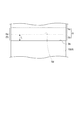
図1及び図2を参照して、半導体装置20の構成を説明する。図1は、実施形態に係る半導体装置20の構成を示す図である。図2は、p型半導体領域3とp側電極5との接合の様子を説明するための図である。半導体装置20は、半導体素子1とサブマウント13とを備える。半導体素子1は、半導体レーザである。
The configuration of the
半導体素子1は、サブマウント13の主面13aに接合されている。半導体素子1は、n型半導体領域2、p型半導体領域3,活性層4、p側電極5、パッド電極12、及び、n側電極6を有する。
The
n型半導体領域2、p型半導体領域3及び活性層4は、六方晶系III族窒化物半導体からなり、GaN系化合物半導体からなることができる。
The n-
n型半導体領域2は、支持基体7及び半導体層8を有する。支持基体7は、n型半導体領域2の裏面2bを含む。支持基体7の表面7aとn型半導体領域2の裏面2bとn型半導体領域2の表面2aとp型半導体領域3の表面3bとは同じ面方位を有する。表面2a、裏面2b、表面3b及び表面7aは、支持基体7を構成する六方晶系III族窒化物半導体の半極性面である。支持基体7は、n側電極6に接している。支持基体7は、n型半導体領域2の裏面2bを介してn側電極6に接している。
The n-
半導体層8は、支持基体7の表面7a上に設けられている。表面7aは、n型半導体領域2の裏面2bの反対側にある。半導体層8は、n型のエピタキシャル層である。半導体層8は、アンドープの層を含むことができる。半導体層8は、支持基体7に接している。
The
p型半導体領域3は、n型半導体領域2の表面2a上に設けられている。p型半導体領域3は、活性層4上に設けられている。p型半導体領域3は、p型のエピタキシャル層である。p型半導体領域3は、半導体層9及びコンタクト層10を有する。p型半導体領域3は、リッジ部3aを有する。リッジ部3aは、p側電極5に至るまで延びている。
The p-
半導体層9は、活性層4上に設けられたp型のエピタキシャル層である。半導体層9は、アンドープの層を含むことができる。
The
コンタクト層10は、p型半導体領域3のリッジ部3aに含まれる。コンタクト層10は、半導体層9上に設けられている。コンタクト層10は、p型のエピタキシャル層である。コンタクト層10は、p型半導体領域3の表面3bを含む。コンタクト層10は、半導体層9に接している。コンタクト層10は、表面3bを介してp側電極5に接している。コンタクト層10は、III族構成元素としてGaを含有する。
The
p型半導体領域3の表面3bの法線軸NAと、支持基体7及びコンタクト層10を構成する六方晶系III族窒化物半導体のc軸CAとの成す角度θは、10度以上80度以下の範囲、及び、100度以上170度以下の範囲、の何れかの範囲内にあることができる。p型半導体領域3の表面3bの法線軸NAと、支持基体7及びコンタクト層10を構成する六方晶系III族窒化物半導体のc軸CAとの成す角度θは、63度以上80度以下の範囲、及び、100度以上117度以下の範囲、の何れかの範囲内にあることができる。
The angle θ formed between the normal axis NA of the
活性層4は、n型半導体領域2の表面2aに設けられている。活性層4は、n型半導体領域2とp型半導体領域3との間に配置されている。活性層4は、n型半導体領域2とp型半導体領域3とに接している。活性層4は、半導体層9に接しており、半導体層8に接している。活性層4は、表面2aを介してn型半導体領域2(具体的には半導体層8)に接している。活性層4は、アンドープのエピタキシャル層である。
The active layer 4 is provided on the
p側電極5は、p型半導体領域3の表面3bに設けられている。p側電極5は、表面3bを介してp型半導体領域3(具体的にはコンタクト層10)に接している。n側電極6は、n型半導体領域2の裏面2bに設けられている。n側電極6は、裏面2bを介してn型半導体領域2に接している。n側電極6は、Al,Pt,Au,Pd,V,Tiの何れかの金属層を含む。
The p-
p側電極5は、Pd,Ni,Auの何れかの金属層5aを含む。金属層5aは、p型半導体領域3(具体的にはコンタクト層10)に接している。金属層5aは、例えば、10nm以上500nm以下の厚みを有する。金属層5aは、例えば、Pd金属層であることができる。また、p側電極5上にはp側電極5を覆うようにパッド電極12が設けられている。パッド電極12は、絶縁層11の表面上に延びている。パッド電極12は、p側電極5及び絶縁層11に接する。パッド電極12は、例えばTi,Auを含む。
The p-
p側電極5は、領域5b及び領域5cから成る。領域5bは、p型半導体領域3の表面3bを介してp型半導体領域3(具体的にはコンタクト層10)に接する部分である。領域5cは、p側電極5から領域5bを除いた領域であり、サブマウント13に接合される部分である。
The p-
領域5bは、p型半導体領域3の表面3bから5nm以上の厚みLを有することができる。領域5bと領域5cとの界面5dは、p型半導体領域3の表面3bから5nm以上離れている。領域5bにおいてp側電極5が含有するGaの量(原子数%)は、半導体素子1がサブマウント13に実装された後においてp型半導体領域3(具体的にはコンタクト層10)が含有するGaの量(原子数%)の3×10⁻⁴倍以下である。界面5dは、金属層5aに含まれる。
領域5bは、p型半導体領域3の表面3bから8nm以上の厚みLを有することができる。この場合、領域5bと領域5cとの界面5dは、p型半導体領域3の表面3bから8nm以上離れている。さらに、この場合、領域5bにおいてp側電極5が含有するGaの量(原子数%)は、半導体素子1がサブマウント13に実装された後においてp型半導体領域3(具体的にはコンタクト層10)が含有するGaの量(原子数%)の2×10⁻⁴倍以下である。
p側電極5とp型半導体領域3との接触面(表面3b)の接触抵抗の値の増加量は、実装後の電圧の上昇量(例えば0.2Vの上昇)から見積もると0.4×10⁻⁴Ωcm2以内(特に、1×10⁻⁵Ωcm2以上1×10⁻⁴Ωcm2以下)である。
The amount of increase in the contact resistance value of the contact surface (
p側電極5(具体的には金属層5a)は、はんだ14を介してサブマウント13の主面13aに接合されている。はんだ14の材料は、例えば、SnAgである。他のはんだ材料として、SnAg、BiSnもあるが、これらはSnの割合90%程度と非常に高く、レーザ動作中にSnの多さに起因したSnのウィスカーの発生が懸念され、信頼性の確保に向かない。サブマウント13の材料は、例えば、AlNである。サブマウントの材料として、銅ダイヤ、ダイヤ、銅タングステンがあるが、放熱性、熱膨張係数の観点から、AlNが最も好ましい。
The p-side electrode 5 (specifically, the
半導体素子1は、絶縁膜11を有する。絶縁層11は、リッジ部3aの側壁を含むp型半導体領域3の表面を覆う。絶縁層11は、例えば、SiO2膜からなることができる。
The
本実施形態に係る半導体装置20では、p型半導体領域3の表面3bから5nm以上離れているp側電極5の領域5cにおいてp側電極5が含有するGaの量(原子数%)は、p型半導体領域3が含有するGaの量(原子数%)の3×10−4倍以下である。半導体素子1のp側電極5をサブマウント13に接合する場合、半導体素子1の温度を上昇させて半導体素子1のp側電極5をサブマウント13にはんだ14を介して接合するが、半導体素子1の温度の上昇に伴い、p側電極5に接するp型半導体領域3のGa原子がp側電極5に拡散し、p型半導体領域3の内部にGa空孔が生じ、キャリア濃度が低減し、よって、p側電極5におけるオーミック性が低減する。本実施形態に係る半導体素子1では、p型半導体領域3からp側電極5に拡散するGa原子の量は、p型半導体領域3が含有するGa原子の量の3×10⁻⁴倍以下であり、欠陥濃度で1×1018cm−3以下とp型ドーピング濃度1×1019cm−3以上よりも比較的低いので、半導体素子1がサブマウント13に実装された後においても、p側電極5におけるオーミック性が十分に維持される。これは、Gaの拡散が抑制されることで、半導体中のGa空孔の濃度が増加しないため、オーミックを得るのに良好なキャリア濃度を確保できるためである。すなわち、Ga空孔が深い準位として働き、自由正孔を捕獲することで、自由正孔濃度を低下させてしまう、ということを抑制するためである。
In the
本実施形態に係る半導体装置20では、p側電極5の領域5cがp型半導体領域3の表面3bから8nm以上離れている場合、p側電極5が含有するGaの量(原子数%)は、p型半導体領域3が含有するGaの量(原子数%)の2×10⁻⁴倍以下である。この場合、p型半導体領域3からp側電極5に拡散するGa原子の量は、p型半導体領域3が含有するGa原子の量の2×10⁻⁴倍以下であり、比較的に低いので、半導体素子1がサブマウント13に実装された後においても、p側電極5におけるオーミック性が十分に維持される。これは、半導体中のGa空孔の濃度で1×1018cm−3以下に相当するので、n型ドーピング濃度1×1019cm−3以上よりも低くGa空孔によるキャリア濃度の低下を無視することが可能となるため、これによる電圧の上昇を抑制することが可能となる。
In the
本実施形態に係る半導体装置20では、n型半導体領域2は、n型半導体領域2の裏面2bを含む支持基体7と、支持基体7の表面7a上に設けられたn型のエピタキシャル層である半導体層8とを含み、支持基体7の表面7aは、n型半導体領域2の裏面2bの反対側にあり、p型半導体領域3は、n型半導体領域2の上に設けられたp型のエピタキシャル層であり、p型半導体領域3のコンタクト層10の表面(p型半導体領域3の表面3b)と支持基体7の表面7aとは同じ面方位を有する。従って、半導体素子1は、半極性面である支持基体7の表面7a上にエピタキシャル成長した積層を有する半導体素子に対して適用可能である。この顕著なGa原子の拡散は、半極性面の不対電子対の多さによる表面エネルギーの不安定性に起因すると考えられるためである。
In the
本実施形態に係る半導体装置20では、p側電極5は、Pd,Ni,Auの何れかの金属層5aを含み、金属層5aは、p型半導体領域3に接しており、金属層5aは、10nm以上500nm以下の厚みを有する。p側電極5の材料には、Pd,Ni,Au等の複数の金属を用いることができる。p側電極5の材料としては、特に、Pdを用いることができる。これらの金属は、仕事関数が高く、また半極性p−GaNと良好な密着性を得ることができるためである。p側電極5の材料としては、特に、Pdを用いることができる。それは、特に仕事関数が高いため、良好なオーミック特性を得ることが可能となるためである。
In the
本実施形態に係る半導体装置20では、p側電極5は、はんだ14を介してサブマウント13の主面13aに接合されており、はんだ14の材料は、SnAgである。よって、比較的に低い温度で半導体素子1をサブマウント13に接合できる。他のはんだ材料として、SnAg、BiSnもあるが、これらはSnの割合90%程度と非常に高く、レーザ動作中にSnの多さに起因したSnのウィスカーの発生が懸念され、信頼性の確保に向かない。
In the
本実施形態に係る半導体装置20では、サブマウント13の材料は、AlNである。サブマウントの材料として、銅ダイヤ、ダイヤ、銅タングステンがあるが、放熱性、熱膨張係数の観点から、AlNが最も好ましい。サブマウント13は比較的に高い熱伝導性を有するので、半導体素子1がサブマウント13に接合される場合に半導体素子1の温度上昇が抑制される。これは、AlNの熱伝導率が230W/mKと高い熱伝導率を有するためである。
In the
本実施形態に係る半導体装置20では、p型半導体領域3の表面3bの法線軸NAと六方晶系III族窒化物半導体のc軸CAとの成す角度θは、10度以上80度以下の範囲、及び、100度以上170度以下の範囲、の何れかの範囲内にある。従って、半導体装置20は、380nm以上600nm以下の波長のレーザ光を出力する半導体レーザに適用できる。この角度における半極性の支持基体7(例えばGaNからなる支持基体)上の量子井戸(活性層4に含まれる量子井戸層であり、例えばInGaNからなる量子井戸)の品質は、380nm以上600nm以下を外れると著しく悪化し、その量子井戸よりも後に成長するエピタキシャル層の結晶性が悪くなり、良好なキャリア濃度を確保することが不可となる。
In the
本実施形態に係る半導体装置20では、p型半導体領域3の表面3bの法線軸NAと六方晶系III族窒化物半導体のc軸CAとの成す角度θは、63度以上80度以下の範囲、及び、100度以上117度以下の範囲、の何れかの範囲内にある。半導体装置20は、380nm以上600nm以下の波長のレーザ光を出力する半導体レーザに適用できる。この角度における半極性の支持基体7(例えばGaNからなる支持基体)であれば、この支持基体7上の量子井戸(活性層4に含まれる量子井戸であり、例えばInGaNからなる量子井戸)の品質は、380nm以上600nm以下であっても、比較的良好な結晶性を保ち、その量子井戸よりも後に成長するエピタキシャル層の結晶性は比較的良くなるため、良好なキャリア濃度を確保することが可能となる。
In the
本実施形態に係る半導体装置20では、p側電極5とp型半導体領域3との接触面(表面3b)の接触抵抗の値は、1×10⁻⁵Ωcm2以上1×10⁻⁴Ωcm2以下である。従って、半導体装置20では、1×10⁻⁵Ωcm2以上1×10⁻⁴Ωcm2以下という比較的に低い接触抵抗値が、p側電極5とp型半導体領域3との接触面において実現できる。これにより、接触抵抗による電圧降下の効果を無視可能となる。
In the
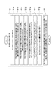
次に、図3を参照して、半導体装置20の作製方法を説明する。図3は、半導体装置20の主要な作製工程を説明する図である。図3に示すように、半導体装置20の作製方法は、ステップS1及びステップS2を有する。ステップS1は、半導体素子1を用意する工程である。ステップS1において用意した半導体素子1は、ステップS2において、サブマウント13に接合される。半導体素子1を用意するステップS1は、ステップS1a,S1b,S1c,S1d,S1e,S1f,S1gを含む。
Next, a method for manufacturing the
(ステップS1a)六方晶系III族窒化物半導体のエピタキシャルウェハを形成する。このエピタキシャルウェハの半導体積層の構造は、図1に示す半導体素子1の半導体積層の構造(例えば、図4に示すエピタキシャルウェハ1_1の半導体積層の構造)と同一である。
(Step S1a) An epitaxial wafer of a hexagonal group III nitride semiconductor is formed. The structure of the semiconductor stack of the epitaxial wafer is the same as the structure of the semiconductor stack of the
ステップS1aの後に、ステップS1b〜S1dにおいて、エピタキシャルウェハのp側の表面にリッジ部とp側電極とを形成する。p側の表面とは、p型の半導体層が設けられている側の表面であり、エピタキシャルウェハのn側の表面の反対側にある。エピタキシャルウェハのn側の表面とは、n型の半導体層が設けられている側の表面である。p側電極は、図1に示す半導体素子1のp側電極5に対応する。
After step S1a, in steps S1b to S1d, a ridge portion and a p-side electrode are formed on the p-side surface of the epitaxial wafer. The p-side surface is the surface on the side where the p-type semiconductor layer is provided, and is on the opposite side of the n-side surface of the epitaxial wafer. The n-side surface of the epitaxial wafer is the surface on the side where the n-type semiconductor layer is provided. The p-side electrode corresponds to the p-
(ステップS1b)エピタキシャルウェハを支持するサセプタの温度を例えば1分程度の間に例えば摂氏100度程度に維持した状態において、リッジ部を形成するためのレジストを、エピタキシャルウェハのp側の表面に、フォトリソグラフィにより形成する。 (Step S1b) In a state where the temperature of the susceptor that supports the epitaxial wafer is maintained at, for example, about 100 degrees Celsius for about 1 minute, a resist for forming the ridge portion is formed on the p-side surface of the epitaxial wafer. It is formed by photolithography.
(ステップS1c)レジストを形成した後に、エピタキシャルウェハを支持するサセプタの温度を例えば10分程度の間に例えば摂氏90度程度に維持した状態において、エピタキシャルウェハのp側の表面に対しドライエッチングを施す。 (Step S1c) After the resist is formed, dry etching is performed on the p-side surface of the epitaxial wafer while maintaining the temperature of the susceptor supporting the epitaxial wafer at, for example, about 90 degrees Celsius for about 10 minutes. .
(ステップS1d)ドライエッチングによりリッジ部(図1に示す半導体素子1のリッジ部3aに対応)が形成された後に、ドライエッチングによって露出したp側の表面とリッジ部の側面とに絶縁層(図1に示す半導体素子1の絶縁層11に対応)を形成する。エピタキシャルウェハのp側の表面は、絶縁層の表面と、リッジ部の端面とを含む。エピタキシャルウェハを支持するサセプタの温度を例えば10分程度の間に例えば摂氏80度程度に維持した状態において、リッジ部の端面にp側電極を形成する。p側電極は、図1に示す半導体素子1のp側電極5に対応する。
(Step S1d) After a ridge portion (corresponding to the
(ステップS1e)p側電極を形成した後に、エピタキシャルウェハを支持するサセプタの温度を例えば5分程度の間に例えば摂氏80度程度に維持した状態において、エピタキシャルウェハのn側の表面を、研磨し、ワックス処理する。 (Step S1e) After the p-side electrode is formed, the surface on the n-side of the epitaxial wafer is polished in a state where the temperature of the susceptor that supports the epitaxial wafer is maintained at, for example, about 80 degrees Celsius for about 5 minutes. , Waxing.
(ステップS1f)エピタキシャルウェハを支持するサセプタの温度を例えば10分程度の間に例えば摂氏80度程度に維持した状態において、エピタキシャルウェハのn側の表面にn側電極を形成する。n側電極は、図1に示す半導体素子1のn側電極6に対応する。
(Step S1f) An n-side electrode is formed on the n-side surface of the epitaxial wafer in a state where the temperature of the susceptor supporting the epitaxial wafer is maintained at, for example, about 80 degrees Celsius for about 10 minutes. The n-side electrode corresponds to the n-side electrode 6 of the
(ステップS1g)エピタキシャルウェハにリッジ部、p側電極及びn側電極が形成された後の基板生産物から、複数の半導体素子を分離する。分離後の半導体素子は、図1に示す半導体素子1である。ステップS1a〜1gが終了し、半導体素子1が用意される。
(Step S1g) A plurality of semiconductor elements are separated from the substrate product after the ridge, p-side electrode, and n-side electrode are formed on the epitaxial wafer. The semiconductor element after separation is the
(ステップS2)サブマウント13の主面13aには、ステップS2の実行前に、予め、はんだ14が設けられている。はんだ14が予め設けられたサブマウント13の主面13aに、半導体素子1のp側電極5を、はんだ14を介して押し当てつつ、例えば摂氏200度以上摂氏205度以下の範囲内に至るまでサブマウント13の主面13aの温度を上げ、予め設定された時間の間(例えば1.5秒以上5.5秒以下の間であるが、特に例えば5秒程度の間とすることができる)だけサブマウント13の主面13aの温度を摂氏200度以上摂氏205度以下の範囲内に維持する。
(Step S2)
ステップS1,S2の後、半導体素子1及びサブマウント13の温度を室温に下げる。以上のようにして、半導体装置20の製造が行われる。
After steps S1 and S2, the temperature of the
半導体素子1のn側電極6をサブマウント13に接合する場合、サブマウント13の主面13aの温度を上昇させて半導体素子1のn側電極6をサブマウント13にはんだ14を介して接合するが、半導体素子1の温度の上昇に伴い、n側電極6に接するn型半導体領域2のGa原子がn側電極6に拡散し、n型半導体領域2の内部にGa空孔が生じ、キャリア濃度が低減し、よって、n側電極6におけるオーミック性が低減する。本実施の形態においては、半導体素子1のn側電極6をサブマウント13に接合する場合、サブマウント13の主面13aの温度を比較的に短い時間である1.5秒以上5.5秒以下の間だけ比較的に低温の摂氏200度以上摂氏205度以下の範囲内に維持するので、半導体素子1の温度上昇が抑制され、n型半導体領域2からn側電極6にGa原子が拡散するのが抑制され、よって、半導体素子1がサブマウント13に実装された後においても、n側電極6におけるオーミック性が十分に維持できる。また、サブマウント13の主面13aには、予めはんだ14が設けられているので、半導体素子1をサブマウント13に容易に接合できる。これにより、短時間での接合が可能で、半導体素子1に与える熱的ダメージを少なくすることができる。
When the n-side electrode 6 of the
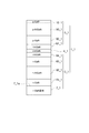
(実施例)図4に、エピタキシャルウェハ1_1の半導体積層を示す。エピタキシャルウェハ1_1は、図3に記載のエピタキシャルウェハ(半導体素子1が得られるエピタキシャルウェハ)の一実施例である。半導体素子1は、エピタキシャルウェハ1_1にリッジ部、p側電極及びn側電極が設けられた基板生産物から、分離されることができる。すなわち、図4に示すエピタキシャルウェハ1_1の半導体積層は、半導体素子1の半導体積層の一実施例でもある。
(Example) FIG. 4 shows a semiconductor lamination of an epitaxial wafer 1_1. Epitaxial wafer 1_1 is an example of the epitaxial wafer shown in FIG. 3 (epitaxial wafer from which
エピタキシャルウェハ1_1の半導体積層を、MOVPE(Metal-Organic Vapor Phase Epitaxy)法によってエピタキシャル成長させて形成した。母体材料の供給ガスとして、トリメチルガリウム(TMG)、トリメチルアルミニウム(TMA)、トリメチルインジウム(TMI)、及び、アンモニア(NH3)を使用した。n型及びp型のドーパントとして、シラン(SiH2)、及び、トリメチルマグネシウム、等を使用した。 The semiconductor stack of the epitaxial wafer 1_1 was formed by epitaxial growth using the MOVPE (Metal-Organic Vapor Phase Epitaxy) method. Trimethylgallium (TMG), trimethylaluminum (TMA), trimethylindium (TMI), and ammonia (NH 3 ) were used as the base material supply gas. Silane (SiH 2 ), trimethyl magnesium, and the like were used as n-type and p-type dopants.
エピタキシャルウェハ1_1の半導体積層は、n型半導体領域2_1(図1に示す半導体素子1のn型半導体領域2に対応)、p型半導体領域3_1(図1に示す半導体素子1のp型半導体領域3に対応)及びi−InGaN層4_1(図1に示す半導体素子1の活性層4に対応)を有する。i−InGaN層4_1は、n型半導体領域2_1とp型半導体領域3_1との間に設けられている。
The semiconductor stack of the epitaxial wafer 1_1 includes an n-type semiconductor region 2_1 (corresponding to the n-
n型半導体領域2_1は、n−GaN基板7_1、n−GaN層81_1、n−AlGaN層82_1、n−GaN層83_1、及び、i−InGaN層84_1を有する。n−GaN基板7_1は、図1に示す半導体素子1の支持基体7に対応する。n−GaN層81_1、n−AlGaN層82_1、n−GaN層83_1、及び、i−InGaN層84_1から成る層は、図1に示す半導体素子1の半導体層8に対応する。n−GaN層81_1は、n型のバッファ層である。n−AlGaN層82_1は、n型のクラッド層である。n−GaN層83_1は、n型の光ガイド層である。i−InGaN層84_1は、アンドープの光ガイド層である。
The n-type semiconductor region 2_1 includes an n-GaN substrate 7_1, an n-GaN layer 81_1, an n-AlGaN layer 82_1, an n-GaN layer 83_1, and an i-InGaN layer 84_1. The n-GaN substrate 7_1 corresponds to the support base 7 of the
p型半導体領域3_1は、i−InGaN層91_1、p−GaN層92_1、p−AlGaN層93_1、及び、p−GaN層10_1を有する。i−InGaN層91_1、p−GaN層92_1、及び、p−AlGaN層93_1から成る層は、図1に示す半導体素子1の半導体層9に対応する。p−GaN層10_1は、図1に示す半導体素子1のコンタクト層10に対応する。i−InGaN層4_1は、図1に示す半導体素子1の活性層4に対応する。i−InGaN層91_1は、アンドープの光ガイド層である。p−GaN層92_1は、p型の光ガイド層である。p−AlGaN層93_1は、p型のクラッド層である。p−GaN層10_1は、マグネシウムが比較的に高濃度にドープされたp+型のコンタクト層である。
The p-type semiconductor region 3_1 includes an i-InGaN layer 91_1, a p-GaN layer 92_1, a p-AlGaN layer 93_1, and a p-GaN layer 10_1. A layer including the i-InGaN layer 91_1, the p-GaN layer 92_1, and the p-AlGaN layer 93_1 corresponds to the
n−GaN基板7_1の主面7_1aの面方位は、半極性の{20−21}であった。n−GaN基板7_1の主面7_1a上に、n−GaN層81_1、n−AlGaN層82_1、n−GaN層83_1、i−InGaN層84_1、i−InGaN層4_1、i−InGaN層91_1、p−GaN層92_1、p−AlGaN層93_1、及び、p−GaN層10_1を、エピタキシャル成長によって、順に形成した。 The plane orientation of the main surface 7_1a of the n-GaN substrate 7_1 was semipolar {20-21}. On the main surface 7_1a of the n-GaN substrate 7_1, an n-GaN layer 81_1, an n-AlGaN layer 82_1, an n-GaN layer 83_1, an i-InGaN layer 84_1, an i-InGaN layer 4_1, an i-InGaN layer 91_1, and a p- A GaN layer 92_1, a p-AlGaN layer 93_1, and a p-GaN layer 10_1 were sequentially formed by epitaxial growth.
n−GaN層81_1は、n−GaN基板7_1の主面7_1aに接している。n−AlGaN層82_1は、n−GaN層81_1に接している。n−GaN層83_1は、n−AlGaN層82_1に接している。i−InGaN層84_1は、n−GaN層83_1に接している。i−InGaN層4_1は、i−InGaN層84_1に接している。i−InGaN層91_1は、i−InGaN層4_1に接している。p−GaN層92_1は、i−InGaN層91_1に接している。p−AlGaN層93_1は、p−GaN層92_1に接している。p−GaN層10_1は、p−AlGaN層93_1に接している。 The n-GaN layer 81_1 is in contact with the main surface 7_1a of the n-GaN substrate 7_1. The n-AlGaN layer 82_1 is in contact with the n-GaN layer 81_1. The n-GaN layer 83_1 is in contact with the n-AlGaN layer 82_1. The i-InGaN layer 84_1 is in contact with the n-GaN layer 83_1. The i-InGaN layer 4_1 is in contact with the i-InGaN layer 84_1. The i-InGaN layer 91_1 is in contact with the i-InGaN layer 4_1. The p-GaN layer 92_1 is in contact with the i-InGaN layer 91_1. The p-AlGaN layer 93_1 is in contact with the p-GaN layer 92_1. The p-GaN layer 10_1 is in contact with the p-AlGaN layer 93_1.
エピタキシャルウェハ1_1の半導体積層の形成後、フォトリソグラフィおよびドライエッチングによって、この半導体積層のp側の表面(p型半導体領域3_1の側)に、リッジ部(図1に示す半導体素子1のリッジ部3aに対応)を形成した。
After the formation of the semiconductor stack of the epitaxial wafer 1_1, the ridge portion (the
リッジ部の形成後、p側の表面にSiO2の絶縁層(図1に示す半導体素子1の絶縁層11に対応)を形成し、そして、露出したリッジ部の端面(図1に示す半導体素子1のp型半導体領域3の表面3bに対応)にp側電極(図1に示す半導体素子1のp側電極5に対応)を形成した。p側電極の形成は、電子ビーム法および抵抗加熱法によって、Pd,Pt,Auを、順に、それぞれ200オングストローム、200オングストローム、5000オングストロームの厚みに形成した。Pdの金属層が、エピタキシャルウェハ1_1のp側の表面(図1に示す半導体素子1の表面3bに対応)に接していた。p側電極の形成後、p側電極を覆うようにパッド電極(図1に示すパッド電極12に対応)を形成した。
After the formation of the ridge portion, an SiO 2 insulating layer (corresponding to the insulating
p側電極及びパッド電極の形成後、エピタキシャルウェハ1_1の半導体積層のn側の表面(n−GaN基板7_1の表面)を、研磨し、ワックス処理した後に、このn側の表面(図1に示す半導体素子1のn型半導体領域2の裏面2bに対応)にn側電極(図1に示す半導体素子1のn側電極6に対応)を形成した。n側電極の形成は、電子ビーム法および抵抗加熱法によって、Al,Ti,Auを、順に、それぞれ200オングストローム、200オングストローム、5000オングストロームの厚みに形成した。Alの金属層が、エピタキシャルウェハ1_1のn側の表面(図1に示す半導体素子1の裏面2bに対応)に接していた。
After the formation of the p-side electrode and the pad electrode, the n-side surface (the surface of the n-GaN substrate 7_1) of the semiconductor stack of the epitaxial wafer 1_1 is polished and waxed, and then the n-side surface (shown in FIG. 1). An n-side electrode (corresponding to the n-side electrode 6 of the
エピタキシャルウェハ1_1にp側電極、パッド電極及びn側電極を形成した後、エピタキシャルウェハ1_1とp側電極とパッド電極とn側電極とからなる基板生産物から、複数の半導体素子(図1に示す半導体素子1に対応)を分離した。 After the p-side electrode, the pad electrode, and the n-side electrode are formed on the epitaxial wafer 1_1, a plurality of semiconductor elements (shown in FIG. 1) are formed from the substrate product including the epitaxial wafer 1_1, the p-side electrode, the pad electrode, and the n-side electrode. Corresponding to the semiconductor element 1).
分離した半導体素子を、AlNのサブマウントの主面(図1に示すサブマウント13の主面13aに対応)に接合した。このサブマウントの主面には、SnAgはんだ(図1に示すはんだ14に対応)が予め蒸着されていた。5秒程度の間にサブマウントの主面の温度を摂氏200度以上240度以下の範囲(具体的には、摂氏200度、摂氏205度、摂氏215度、摂氏225度、摂氏230度、摂氏240度)に維持した状態で、SnAgはんだを介して、半導体素子のp側にあるパッド電極(図1に示すパッド電極12に対応)をサブマウントの主面に接合した。
The separated semiconductor element was joined to the main surface of the AlN submount (corresponding to the
半導体素子をサブマウントに接合した後、半導体素子の順方向の動作電圧(50mAの動作電圧)を測定した。半導体素子をサブマウントに実装する前にも、半導体素子の順方向の動作電圧(50mAの動作電圧)を予め測定しておき、半導体素子をサブマウントに接合する前と後とにおける順方向の動作電圧の変化(動作電圧の上昇量)を評価した。半導体素子への電圧の印加は、電圧上昇による半導体素子の発熱の影響を低減するために、0.5μs/100μs(オンとなる期間/パルス周期);デューティ比0.5%、というパルス条件を満たすものであった。 After bonding the semiconductor element to the submount, the forward operating voltage (50 mA operating voltage) of the semiconductor element was measured. Before the semiconductor element is mounted on the submount, the forward operating voltage (50 mA operating voltage) of the semiconductor element is measured in advance, and the forward operation before and after the semiconductor element is bonded to the submount. The change in voltage (amount of increase in operating voltage) was evaluated. In order to reduce the influence of heat generation of the semiconductor element due to the voltage increase, the application of voltage to the semiconductor element is performed under the pulse condition of 0.5 μs / 100 μs (ON period / pulse period); duty ratio 0.5%. It was something to satisfy.
図5に、半導体素子の動作電圧の上昇量についての評価結果を示す。図5の横軸は、半導体素子をサブマウントの主面に接合する時のサブマウントの主面の温度(実装温度)を示し、図5の縦軸は、半導体素子の動作電圧(50mAの動作電圧)の上昇量を示す。図5に示すように、実装温度が高くなるほど、半導体素子の動作電圧(50mAの動作電圧)の上昇量も増加する。実装温度が摂氏200度、摂氏205度の場合、半導体素子の動作電圧の上昇量は0.2Vを下回っており、実装温度が摂氏215度、摂氏225度の場合、半導体素子の動作電圧の上昇量は0.1V以上0.4V以下の範囲にあり、実装温度が摂氏230度の場合、半導体素子の動作電圧の上昇量は0.2V以上0.5V以下の範囲にあり、実装温度が摂氏240度の場合、半導体素子の動作電圧の上昇量は0.6Vを越えた。このように、実装温度が摂氏200度、摂氏205度と比較的に低い場合には、半導体素子の動作電圧の上昇量も比較的に低い、という結果を得た。 FIG. 5 shows the evaluation results for the amount of increase in the operating voltage of the semiconductor element. 5 indicates the temperature (mounting temperature) of the main surface of the submount when the semiconductor element is bonded to the main surface of the submount, and the vertical axis of FIG. 5 indicates the operating voltage (50 mA operation of the semiconductor device). (Voltage) increase. As shown in FIG. 5, as the mounting temperature increases, the amount of increase in the operating voltage of the semiconductor element (50 mA operating voltage) also increases. When the mounting temperature is 200 degrees Celsius and 205 degrees Celsius, the amount of increase in the operating voltage of the semiconductor element is less than 0.2V, and when the mounting temperature is 215 degrees Celsius and 225 degrees Celsius, the operating voltage of the semiconductor element is increased. When the amount is in the range of 0.1V to 0.4V and the mounting temperature is 230 degrees Celsius, the increase in the operating voltage of the semiconductor element is in the range of 0.2V to 0.5V, and the mounting temperature is in Celsius In the case of 240 degrees, the amount of increase in the operating voltage of the semiconductor element exceeded 0.6V. Thus, when the mounting temperature is relatively low, such as 200 degrees Celsius and 205 degrees Celsius, the increase in the operating voltage of the semiconductor element is relatively low.
上記の結果の原因を知得するため、本実施例に係る半導体素子に対しSIMS分析を実施した。摂氏205度の実装温度でサブマウントの主面に接合した半導体素子(実施例1)と、摂氏240度の実装温度でサブマウントの主面に接合した半導体素子(実施例2)とを、サブマウントへの接合の後に、サブマウントから機械的に分離し、実施例1の半導体素子と実施例2の半導体素子のそれぞれに対し、p側電極からSIMS測定を行った。実施例1,2は、何れも、本実施例に係る半極性GaN基板(具体的には上記したように{20−21}面のGaN基板)のエピタキシャルウェハ1_1から得られる半導体素子であるが、p側電極の形状を円形状とし、p側電極のAu金属層の厚みを2000オングストロームとした。図5に示すように、実施例1の場合には半導体素子の動作電圧の上昇量は比較的に小さく、実施例2の場合には半導体素子の動作電圧の上昇量が比較的に大きい。
In order to know the cause of the above results, SIMS analysis was performed on the semiconductor element according to this example. A semiconductor element (Example 1) bonded to the main surface of the submount at a mounting temperature of 205 degrees Celsius and a semiconductor element (Example 2) bonded to the main surface of the submount at a mounting temperature of 240 degrees Celsius After joining to the mount, it was mechanically separated from the submount, and SIMS measurement was performed from the p-side electrode for each of the semiconductor element of Example 1 and the semiconductor element of Example 2. Examples 1 and 2 are both semiconductor elements obtained from the epitaxial wafer 1_1 of the semipolar GaN substrate according to this example (specifically, as described above, the {20-21} -plane GaN substrate). The shape of the p-side electrode was circular, and the thickness of the Au metal layer of the p-side electrode was 2000 angstroms. As shown in FIG. 5, in the case of the first embodiment, the increase amount of the operating voltage of the semiconductor element is relatively small, and in the case of the
実施例1,2に対するSIMS測定の結果を図6に示す。図6の横軸は、p側電極とp型半導体領域との界面からの距離を示しており、距離がマイナスの値となっている領域は、p側電極の内部に対応している。図6の縦軸は、実施例1,2におけるGa原子及びPd原子の含有量を示す。Ga原子の含有量については、p型半導体領域の(特に、p側電極との界面の近傍における)Ga原子の含有量(原子数%)を1とした場合の値を示している。Pd原子の含有量については、p側電極の(特に、p型半導体領域との界面の近傍における)Pd原子の含有量(原子数%)を1とした場合の値を示している。図6に示すGa原子及びPd原子の含有量の測定は、サブマウントに半導体素子を接合した後に行った。図6のグラフG1は、実施例1におけるPd原子の含有量を示し、グラフG2は、実施例2におけるPd原子の含有量を示している。図6のグラフG3は、実施例1におけるGa原子の含有量を示し、グラフG4は、実施例2におけるGa原子の含有量を示している。 The results of SIMS measurement for Examples 1 and 2 are shown in FIG. The horizontal axis of FIG. 6 indicates the distance from the interface between the p-side electrode and the p-type semiconductor region, and the region where the distance is a negative value corresponds to the inside of the p-side electrode. The vertical axis | shaft of FIG. 6 shows content of Ga atom and Pd atom in Example 1,2. The Ga atom content is a value when the Ga atom content (number of atoms in%) of the p-type semiconductor region (particularly in the vicinity of the interface with the p-side electrode) is 1. The Pd atom content is a value when the Pd atom content (number of atoms%) of the p-side electrode (particularly in the vicinity of the interface with the p-type semiconductor region) is 1. The measurement of the content of Ga atoms and Pd atoms shown in FIG. 6 was performed after joining the semiconductor element to the submount. The graph G1 in FIG. 6 shows the content of Pd atoms in Example 1, and the graph G2 shows the content of Pd atoms in Example 2. A graph G3 in FIG. 6 shows the content of Ga atoms in Example 1, and a graph G4 shows the content of Ga atoms in Example 2.
図6に示すように、p側電極とp型半導体領域との界面から8nmまでのp側電極の領域におけるGa原子の含有量は、実施例2の場合、0.1%(図6の縦軸に示す値)以上であるが、実施例1の場合、0.1%(図6の縦軸に示す値)を下回っておりSIMSの検出限界に近いものであった。p側電極とp型半導体領域との界面から5nmまでのp側電極の領域におけるGa原子の含有量も、実施例2の場合、0.1%(図6の縦軸に示す値)以上であるが、実施例1の場合、0.1%(図6の縦軸に示す値)を下回っておりSIMSの検出限界に近いものであった。図6に示す結果を鑑みると、実施例2の場合、p型半導体領域からp側電極にGa原子が拡散したことによってp型半導体領域にGa空孔が発生し、このGa空孔によってp型半導体領域に深い準位(濃度:1×1019cm−3のオーダ)が形成され、その結果、p型半導体領域のキャリア濃度が低下し、よって、動作電圧の上昇量が比較的に大きいものとなったと考えられる。 As shown in FIG. 6, the Ga atom content in the p-side electrode region from the interface between the p-side electrode and the p-type semiconductor region to 8 nm is 0.1% in the case of Example 2 (vertical length in FIG. 6). In the case of Example 1, it was less than 0.1% (value shown on the vertical axis in FIG. 6) and was close to the SIMS detection limit. In the case of Example 2, the Ga atom content in the p-side electrode region from the interface between the p-side electrode and the p-type semiconductor region to 5 nm is also 0.1% (value shown on the vertical axis in FIG. 6) or more. However, in the case of Example 1, it was below 0.1% (value shown on the vertical axis in FIG. 6), which was close to the SIMS detection limit. In view of the result shown in FIG. 6, in the case of Example 2, Ga vacancies are generated in the p-type semiconductor region due to the diffusion of Ga atoms from the p-type semiconductor region to the p-side electrode, and the Ga vacancies cause p-type. A deep level (concentration on the order of 1 × 10 19 cm −3 ) is formed in the semiconductor region, and as a result, the carrier concentration in the p-type semiconductor region is lowered, and thus the amount of increase in operating voltage is relatively large. It is thought that it became.
p側電極内に0.1%のGa原子の拡散がある場合、半導体コンタクト層のGa原子が0.1%(図6の縦軸に示す値)は抜けていることを意味しており、つまりコンタクト層に0.1%以上のGa空孔が発生していることを意味する。このGa空孔の濃度は、1019cm−3以上のオーダであり、1020cm−3のオーダのp型ドーパント濃度に匹敵し、1019cm−3のオーダの有効アクセプタ濃度と同等であり、この場合には自由ホール濃度が著しく低下している。このような自由ホール濃度の低下を改善するには、Ga空孔の濃度を、有効アクセプタ濃度の低下を無視できる程度、すなわち、有効アクセプタ濃度よりも一桁以上低い濃度であれば良い。そのため、p側電極5内のGa濃度で示すと0.1%(図6の縦軸に示す値)以下であれば、有効アクセプタ濃度の減少を無視でき、良好な電気特性を確保することが可能となる。
When there is 0.1% Ga atom diffusion in the p-side electrode, it means that 0.1% Ga atom in the semiconductor contact layer (value shown on the vertical axis in FIG. 6) is missing, That is, it means that 0.1% or more Ga vacancies are generated in the contact layer. The concentration of Ga vacancies is on the order of 10 19 cm −3 or higher, comparable to the p-type dopant concentration on the order of 10 20 cm −3 , and equivalent to the effective acceptor concentration on the order of 10 19 cm −3 . In this case, the free hole concentration is significantly reduced. In order to improve such a decrease in free hole concentration, the Ga vacancy concentration may be set to a level that can ignore the decrease in effective acceptor concentration, that is, a concentration that is lower by one digit or more than the effective acceptor concentration. Therefore, when the Ga concentration in the p-
半極性面GaN基板のエピタキシャルウェハから得られる実施例2のように、実装温度が比較的に高い場合にp型半導体領域からp側電極にGa原子が比較的に大きく拡散する現象は、c面GaN基板のエピタキシャルウェハから得られる半導体素子においては、確認されなかった。半極性面ではGa、Nのダングリングボンドが非常に多いことが一因であると考えられる。すなわち、図6に示す結果は、半極性面に特有の性質である結晶表面の不安定性に起因した現象と考えられる。このように、本実施例において、p型半導体領域に接するp側電極の金属層(オーミック金属)にPdを用い、このPd金属層においてGa原子が比較的に大きく拡散することによって、図6に示すような半導体素子の動作電圧の上昇量が比較的に大きくなる。 The phenomenon that Ga atoms diffuse relatively large from the p-type semiconductor region to the p-side electrode when the mounting temperature is relatively high, as in Example 2 obtained from the epitaxial wafer of the semipolar plane GaN substrate, is the c-plane. It was not confirmed in the semiconductor element obtained from the epitaxial wafer of the GaN substrate. The semipolar plane is thought to be partly due to the large number of dangling bonds of Ga and N. That is, the result shown in FIG. 6 is considered to be a phenomenon caused by instability of the crystal surface, which is a characteristic characteristic of the semipolar plane. As described above, in this example, Pd is used for the metal layer (ohmic metal) of the p-side electrode in contact with the p-type semiconductor region, and Ga atoms diffuse relatively large in this Pd metal layer. As shown, the amount of increase in the operating voltage of the semiconductor element is relatively large.
このような現象は、p型半導体領域からGa原子が抜けp型半導体領域にGa空孔が発生することによって生じるものと考えられるので、p型半導体領域に接する金属層の金属の種類にはよらずに生じるものと考えられる。よって、本実施例のオーミック金属であるPdを、Ni,Auに替えても、p型半導体領域からGa原子が抜けてp型半導体領域にGa空孔が発生する場合には、本実施例と同様の現象、すなわち、本実施例のPdの場合と同様にp側電極内のGa原子の含有量が0.1%(図6の縦軸に示す値)を上回る、という現象が生じると考えられる。さらに、本実施例と同様の現象は、本実施例の場合のような窒化物半導体レーザにのみ生じるものではなく、窒化物半導体発光素子や窒化物半導体受光素子などにおいても生じるものと考えられる。 Such a phenomenon is considered to occur when Ga atoms are removed from the p-type semiconductor region and Ga vacancies are generated in the p-type semiconductor region. Therefore, it depends on the type of metal in the metal layer in contact with the p-type semiconductor region. It is thought that it occurs without. Therefore, even if Pd, which is the ohmic metal of this embodiment, is replaced with Ni or Au, if Ga atoms escape from the p-type semiconductor region and Ga vacancies are generated in the p-type semiconductor region, The same phenomenon, that is, the phenomenon that the Ga atom content in the p-side electrode exceeds 0.1% (value shown on the vertical axis in FIG. 6) occurs as in the case of Pd in this example. It is done. Furthermore, it is considered that the same phenomenon as in this embodiment does not occur only in the nitride semiconductor laser as in this embodiment, but also occurs in the nitride semiconductor light emitting element, the nitride semiconductor light receiving element, and the like.
以上、好適な実施の形態において本発明の原理を図示し説明してきたが、本発明は、そのような原理から逸脱することなく配置および詳細において変更され得ることは、当業者によって認識される。本発明は、本実施の形態に開示された特定の構成に限定されるものではない。したがって、特許請求の範囲およびその精神の範囲から来る全ての修正および変更に権利を請求する。 While the principles of the invention have been illustrated and described in the preferred embodiments, it will be appreciated by those skilled in the art that the invention can be modified in arrangement and detail without departing from such principles. The present invention is not limited to the specific configuration disclosed in the present embodiment. We therefore claim all modifications and changes that come within the scope and spirit of the following claims.
1…半導体素子、10…コンタクト層、10_1…p−GaN層、11…絶縁層、12…パッド電極、13…サブマウント、13a…主面、14…はんだ、1_1…エピタキシャルウェハ、2…n型半導体領域、20…半導体装置、2a…表面、2b…裏面、2_1…n型半導体領域、3…p型半導体領域、3a…リッジ部、3b…表面、3_1…p型半導体領域、4…活性層、4_1…i−InGaN層、5…p側電極、5a…金属層、5b…領域、5c…領域、5d…界面、6…n側電極、7…支持基体、7a…表面、7_1…n−GaN基板、7_1a…主面、8…半導体層、81_1…n−GaN層、82_1…n−AlGaN層、83_1…n−GaN層、84_1…i−InGaN層、9…半導体層、91_1…i−InGaN層、92_1…p−GaN層、93_1…p−AlGaN層、CA…c軸、L…厚み、NA…法線軸。
DESCRIPTION OF
Claims (14)
前記半導体素子を用意する工程と、
前記半導体素子を前記サブマウントの主面に接合する工程と、
を備え、
前記半導体素子は、n型半導体領域と、前記n型半導体領域の表面上に設けられたp型半導体領域と、前記p型半導体領域の表面に設けられPd,Ni,Auの何れかの金属層を含むp側電極と、前記n型半導体領域の裏面に設けられたn側電極とを有し、
前記金属層は、前記p型半導体領域に接しており、
前記金属層は、10nm以上500nm以下の厚みを有し、
n型半導体領域と、p型半導体領域とは、六方晶系III族窒化物半導体からなり、
前記p型半導体領域は、コンタクト層を有し、
前記コンタクト層は、前記p型半導体領域の前記表面を含み、
前記コンタクト層は、前記p側電極に接し、
前記コンタクト層の前記六方晶系III族窒化物半導体はGaNであり、
前記p型半導体領域の前記表面の法線軸と前記六方晶系III族窒化物半導体のc軸との成す角度は、10度以上80度以下の範囲、及び、100度以上170度以下の範囲、の何れかの範囲内にあり、
前記半導体素子を前記サブマウントの前記主面に接合する工程では、前記p側電極をSnAgはんだを介して前記サブマウントの前記主面に押し当てつつ前記サブマウントの前記主面の温度が摂氏200度以上摂氏205度以下の範囲内に至るまで前記サブマウントの前記主面の温度を上げ、1.5秒以上5.5秒以下の間だけ前記サブマウントの前記主面の温度を前記範囲内に維持することにより、前記p型半導体領域の前記表面から5nm以上離れている前記p側電極の領域において前記p側電極が含有するGaの量(原子数%)を、前記コンタクト層が含有するGaの量(原子数%)の3×10 −4 倍以下とする、
ことを特徴とする半導体装置の作製方法。 A method for manufacturing a semiconductor device including a semiconductor element and a submount,
Preparing the semiconductor element;
Bonding the semiconductor element to the main surface of the submount;
With
The semiconductor element includes an n-type semiconductor region, a p-type semiconductor region provided on the surface of the n-type semiconductor region, and a metal layer of any one of Pd, Ni, and Au provided on the surface of the p-type semiconductor region. And a p-side electrode including the n-side electrode provided on the back surface of the n-type semiconductor region,
The metal layer is in contact with the p-type semiconductor region;
The metal layer has a thickness of 10 nm to 500 nm,
The n-type semiconductor region and the p-type semiconductor region are made of a hexagonal group III nitride semiconductor,
The p-type semiconductor region has a contact layer;
The contact layer includes the surface of the p-type semiconductor region;
The contact layer is in contact with the p-side electrode;
The hexagonal group III nitride semiconductor of the contact layer is GaN;
The angle formed between the normal axis of the surface of the p-type semiconductor region and the c-axis of the hexagonal group III nitride semiconductor is in the range of 10 degrees to 80 degrees, and in the range of 100 degrees to 170 degrees, In the range of
In the step of bonding the semiconductor element to the main surface of the submount, the temperature of the main surface of the submount is 200 degrees Celsius while pressing the p-side electrode against the main surface of the submount via SnAg solder. The temperature of the main surface of the submount is increased until the temperature is within a range of not less than 205 degrees Celsius and not more than 205 degrees Celsius, and the temperature of the main surface of the submount is within the range for only 1.5 seconds to 5.5 seconds. By maintaining the thickness of the p-type semiconductor region, the contact layer contains the amount of Ga (atomic%) contained in the p-side electrode in the p-side electrode region that is 5 nm or more away from the surface of the p-type semiconductor region. 3 × 10 −4 times or less the amount of Ga (number of atoms%) ,
A method for manufacturing a semiconductor device.
前記支持基体の前記表面は、前記n型半導体領域の前記裏面の反対側にあり、
前記p型半導体領域は、前記n型半導体領域の上に設けられたp型のエピタキシャル層であり、
前記コンタクト層の前記表面と前記支持基体の前記表面とは同じ面方位を有する、
ことを特徴とする請求項1に記載の半導体装置の作製方法。 The n-type semiconductor region includes a support base including the back surface of the n-type semiconductor region, and an n-type epitaxial layer provided on the surface of the support base,
The front surface of the support base is opposite to the back surface of the n-type semiconductor region;
The p-type semiconductor region is a p-type epitaxial layer provided on the n-type semiconductor region,
The surface of the contact layer and the surface of the support substrate have the same plane orientation;
The method for manufacturing a semiconductor device according to claim 1.
前記Pd金属層は、前記p型半導体領域に接しており、
前記Pd金属層は、10nm以上500nm以下の厚みを有する、
ことを特徴とする請求項1または2に記載の半導体装置の作製方法。 The p-side electrode includes a Pd metal layer,
The Pd metal layer is in contact with the p-type semiconductor region;
The Pd metal layer has a thickness of 10 nm to 500 nm;
The method for manufacturing a semiconductor device according to claim 1 or 2, characterized in that.
ことを特徴とする請求項1〜3の何れか一項に記載の半導体装置の作製方法。 The solder is provided in advance on the main surface of the submount before the step of bonding the semiconductor element to the main surface of the submount is performed.
The method for manufacturing a semiconductor device according to any one of claims 1 to 3 .
前記活性層は、六方晶系III族窒化物半導体からなり、前記n型半導体領域と前記p型半導体領域との間に設けられている、ことを特徴とする請求項1〜5の何れか一項に記載の半導体装置の作製方法。 The semiconductor element is a semiconductor laser having an active layer,
The active layer is made of hexagonal Group III nitride semiconductor, the n-type semiconductor region and is provided between the p-type semiconductor region, any one of claims 1-5, characterized in that A method for manufacturing a semiconductor device according to the item.
前記半導体素子は、n型半導体領域と、前記n型半導体領域の表面上に設けられたp型半導体領域と、前記p型半導体領域の表面に設けられPd,Ni,Auの何れかの金属層を含むp側電極と、前記n型半導体領域の裏面に設けられたn側電極とを有し、
前記金属層は、前記p型半導体領域に接しており、
前記金属層は、10nm以上500nm以下の厚みを有し、
n型半導体領域と、p型半導体領域とは、六方晶系III族窒化物半導体からなり、
前記p側電極は、SnAgはんだを介して前記サブマウントの主面に接合されており、
前記p型半導体領域は、コンタクト層を有し、
前記コンタクト層は、前記p型半導体領域の前記表面を含み、
前記コンタクト層の前記六方晶系III族窒化物半導体はGaNであり、
前記p型半導体領域の前記表面の法線軸と前記六方晶系III族窒化物半導体のc軸との成す角度は、10度以上80度以下の範囲、及び、100度以上170度以下の範囲、の何れかの範囲内にあり、
前記p型半導体領域の前記表面から5nm以上離れている前記p側電極の領域において前記p側電極が含有するGaの量(原子数%)は、前記コンタクト層が含有するGaの量(原子数%)の3×10⁻⁴倍以下である、
ことを特徴とする半導体装置。 A semiconductor device comprising a semiconductor element and a submount,
The semiconductor element includes an n-type semiconductor region, a p-type semiconductor region provided on the surface of the n-type semiconductor region, and a metal layer of any one of Pd, Ni, and Au provided on the surface of the p-type semiconductor region. And a p-side electrode including the n-side electrode provided on the back surface of the n-type semiconductor region,
The metal layer is in contact with the p-type semiconductor region;
The metal layer has a thickness of 10 nm to 500 nm,
The n-type semiconductor region and the p-type semiconductor region are made of a hexagonal group III nitride semiconductor,
The p-side electrode is joined to the main surface of the submount via SnAg solder,
The p-type semiconductor region has a contact layer;
The contact layer includes the surface of the p-type semiconductor region;
The hexagonal group III nitride semiconductor of the contact layer is GaN;
The angle formed between the normal axis of the surface of the p-type semiconductor region and the c-axis of the hexagonal group III nitride semiconductor is in the range of 10 degrees to 80 degrees, and in the range of 100 degrees to 170 degrees, In the range of
The amount (number of atoms%) of Ga contained in the p-side electrode in the region of the p-side electrode 5 nm or more away from the surface of the p-type semiconductor region is the amount of Ga (number of atoms) contained in the contact layer. %) 3 × 10 −4 times or less,
A semiconductor device.
前記支持基体の前記表面は、前記n型半導体領域の前記裏面の反対側にあり、
前記p型半導体領域は、前記n型半導体領域の上に設けられたp型のエピタキシャル層であり、
前記コンタクト層の前記表面と前記支持基体の前記表面とは同じ面方位を有する、
ことを特徴とする請求項8又は9に記載の半導体装置。 The n-type semiconductor region includes a support base including the back surface of the n-type semiconductor region, and an n-type epitaxial layer provided on the surface of the support base,
The front surface of the support base is opposite to the back surface of the n-type semiconductor region;
The p-type semiconductor region is a p-type epitaxial layer provided on the n-type semiconductor region,
The surface of the contact layer and the surface of the support substrate have the same plane orientation;
10. The semiconductor device according to claim 8 , wherein
前記Pd金属層は、前記p型半導体領域に接しており、
前記Pd金属層は、10nm以上500nm以下の厚みを有する、
ことを特徴とする請求項8〜10の何れか一項に記載の半導体装置。 The p-side electrode includes a Pd metal layer,
The Pd metal layer is in contact with the p-type semiconductor region;
The Pd metal layer has a thickness of 10 nm to 500 nm;
The semiconductor device according to claim 8 , wherein the semiconductor device is a semiconductor device.
前記活性層は、六方晶系III族窒化物半導体からなり、前記n型半導体領域と前記p型半導体領域との間に設けられている、ことを特徴とする請求項8〜12の何れか一項に記載の半導体装置。 The semiconductor element is a semiconductor laser having an active layer,
The active layer is made of hexagonal Group III nitride semiconductor, the n-type semiconductor region and is provided between the p-type semiconductor region, any one of claims 8 to 12, characterized in that The semiconductor device according to item.
Priority Applications (1)
| Application Number | Priority Date | Filing Date | Title |
|---|---|---|---|
| JP2012035411A JP5556830B2 (en) | 2012-02-21 | 2012-02-21 | Semiconductor device and manufacturing method of semiconductor device |
Applications Claiming Priority (1)
| Application Number | Priority Date | Filing Date | Title |
|---|---|---|---|
| JP2012035411A JP5556830B2 (en) | 2012-02-21 | 2012-02-21 | Semiconductor device and manufacturing method of semiconductor device |
Publications (2)
| Publication Number | Publication Date |
|---|---|
| JP2013172024A JP2013172024A (en) | 2013-09-02 |
| JP5556830B2 true JP5556830B2 (en) | 2014-07-23 |
Family
ID=49265782
Family Applications (1)
| Application Number | Title | Priority Date | Filing Date |
|---|---|---|---|
| JP2012035411A Expired - Fee Related JP5556830B2 (en) | 2012-02-21 | 2012-02-21 | Semiconductor device and manufacturing method of semiconductor device |
Country Status (1)
| Country | Link |
|---|---|
| JP (1) | JP5556830B2 (en) |
Family Cites Families (8)
| Publication number | Priority date | Publication date | Assignee | Title |
|---|---|---|---|---|
| JPH11233890A (en) * | 1998-02-12 | 1999-08-27 | Matsushita Electric Ind Co Ltd | Gallium nitride based compound semiconductor device |
| JP5028217B2 (en) * | 2007-10-29 | 2012-09-19 | 日立協和エンジニアリング株式会社 | Optical device mounting method |
| JP5280119B2 (en) * | 2008-06-30 | 2013-09-04 | 日本オクラロ株式会社 | Semiconductor laser device |
| JP5258275B2 (en) * | 2007-12-07 | 2013-08-07 | 三菱電機株式会社 | Nitride semiconductor device and manufacturing method thereof |
| JP2009212343A (en) * | 2008-03-05 | 2009-09-17 | Rohm Co Ltd | Nitride semiconductor element, and method of manufacturing the same |
| JP4772135B2 (en) * | 2008-06-09 | 2011-09-14 | ルネサスエレクトロニクス株式会社 | Semiconductor device and manufacturing method thereof |
| JP2010166023A (en) * | 2008-09-30 | 2010-07-29 | Sanyo Electric Co Ltd | Semiconductor laser device and display device |
| JP2011023628A (en) * | 2009-07-17 | 2011-02-03 | Mitsubishi Electric Corp | Semiconductor laser device |
-
2012
- 2012-02-21 JP JP2012035411A patent/JP5556830B2/en not_active Expired - Fee Related
Also Published As
| Publication number | Publication date |
|---|---|
| JP2013172024A (en) | 2013-09-02 |
Similar Documents
| Publication | Publication Date | Title |
|---|---|---|
| US8470627B2 (en) | Method for manufacturing semiconductor light emitting device | |
| US20090179215A1 (en) | Semiconductor light emitting device and fabrication method for the semiconductor light emitting device | |
| US8546167B2 (en) | Gallium nitride-based compound semiconductor light-emitting element | |
| JP5401145B2 (en) | Method for producing group III nitride laminate | |
| JPWO2015146069A1 (en) | Light emitting diode element | |
| WO2014167773A1 (en) | Semiconductor light emitting element and method for manufacturing same | |
| JP5873260B2 (en) | Method for producing group III nitride laminate | |
| CN101667614A (en) | Light emitting diode device and manufacturing method thereof | |
| US7456445B2 (en) | Group III nitride semiconductor light emitting device | |
| JP4103309B2 (en) | Method for manufacturing p-type nitride semiconductor | |
| JP2008288532A (en) | Nitride semiconductor device | |
| JP4034015B2 (en) | Group III nitride compound semiconductor light emitting device | |
| JP5839293B2 (en) | Nitride light emitting device and manufacturing method thereof | |
| JP5556830B2 (en) | Semiconductor device and manufacturing method of semiconductor device | |
| JP6103268B2 (en) | Nitride light emitting device and manufacturing method thereof | |
| JP2009266963A (en) | Nitride-based light emitting device, and method of manufacturing semiconductor light emitting device | |
| JP2004200671A (en) | Semiconductor optical device having quantum well structure and method of manufacturing the same | |
| JP4304984B2 (en) | Nitride semiconductor growth substrate and nitride semiconductor device using the same | |
| JP4720519B2 (en) | Method for manufacturing p-type nitride semiconductor | |
| JP4781028B2 (en) | Group III nitride semiconductor laminate and method for manufacturing group III nitride semiconductor light emitting device | |
| JP2013172012A (en) | Semiconductor device and semiconductor device manufacturing method | |
| JP2005340762A (en) | Group iii nitride semiconductor light-emitting element | |
| JP2000332365A (en) | Semiconductor light emitting device and method of manufacturing the same | |
| JP5898656B2 (en) | Group III nitride semiconductor device | |
| JP2004179613A (en) | Manufacturing method of light emitting device, and light emitting device |
Legal Events
| Date | Code | Title | Description |
|---|---|---|---|
| A977 | Report on retrieval |
Free format text: JAPANESE INTERMEDIATE CODE: A971007 Effective date: 20131227 |
|
| A131 | Notification of reasons for refusal |
Free format text: JAPANESE INTERMEDIATE CODE: A131 Effective date: 20140121 |
|
| A521 | Written amendment |
Free format text: JAPANESE INTERMEDIATE CODE: A523 Effective date: 20140305 |
|
| TRDD | Decision of grant or rejection written | ||
| A01 | Written decision to grant a patent or to grant a registration (utility model) |
Free format text: JAPANESE INTERMEDIATE CODE: A01 Effective date: 20140507 |
|
| A61 | First payment of annual fees (during grant procedure) |
Free format text: JAPANESE INTERMEDIATE CODE: A61 Effective date: 20140520 |
|
| R150 | Certificate of patent or registration of utility model |
Ref document number: 5556830 Country of ref document: JP Free format text: JAPANESE INTERMEDIATE CODE: R150 |
|
| LAPS | Cancellation because of no payment of annual fees |