JP5583324B2 - 埋設された複数の軟質導電性バンプを備えた素子、ならびに、そのような素子と、複数の硬質導電性ポイントを備えた素子と、の電気的接続方法 - Google Patents
埋設された複数の軟質導電性バンプを備えた素子、ならびに、そのような素子と、複数の硬質導電性ポイントを備えた素子と、の電気的接続方法 Download PDFInfo
- Publication number
- JP5583324B2 JP5583324B2 JP2007534065A JP2007534065A JP5583324B2 JP 5583324 B2 JP5583324 B2 JP 5583324B2 JP 2007534065 A JP2007534065 A JP 2007534065A JP 2007534065 A JP2007534065 A JP 2007534065A JP 5583324 B2 JP5583324 B2 JP 5583324B2
- Authority
- JP
- Japan
- Prior art keywords
- pads
- bump
- forming
- points
- conductive
- Prior art date
- Legal status (The legal status is an assumption and is not a legal conclusion. Google has not performed a legal analysis and makes no representation as to the accuracy of the status listed.)
- Expired - Fee Related
Links
Images








Classifications
-
- H—ELECTRICITY
- H10—SEMICONDUCTOR DEVICES; ELECTRIC SOLID-STATE DEVICES NOT OTHERWISE PROVIDED FOR
- H10W—GENERIC PACKAGES, INTERCONNECTIONS, CONNECTORS OR OTHER CONSTRUCTIONAL DETAILS OF DEVICES COVERED BY CLASS H10
- H10W72/00—Interconnections or connectors in packages
-
- H—ELECTRICITY
- H05—ELECTRIC TECHNIQUES NOT OTHERWISE PROVIDED FOR
- H05K—PRINTED CIRCUITS; CASINGS OR CONSTRUCTIONAL DETAILS OF ELECTRIC APPARATUS; MANUFACTURE OF ASSEMBLAGES OF ELECTRICAL COMPONENTS
- H05K3/00—Apparatus or processes for manufacturing printed circuits
- H05K3/30—Assembling printed circuits with electric components, e.g. with resistors
- H05K3/32—Assembling printed circuits with electric components, e.g. with resistors electrically connecting electric components or wires to printed circuits
- H05K3/321—Assembling printed circuits with electric components, e.g. with resistors electrically connecting electric components or wires to printed circuits by conductive adhesives
-
- H—ELECTRICITY
- H05—ELECTRIC TECHNIQUES NOT OTHERWISE PROVIDED FOR
- H05K—PRINTED CIRCUITS; CASINGS OR CONSTRUCTIONAL DETAILS OF ELECTRIC APPARATUS; MANUFACTURE OF ASSEMBLAGES OF ELECTRICAL COMPONENTS
- H05K2201/00—Indexing scheme relating to printed circuits covered by H05K1/00
- H05K2201/03—Conductive materials
- H05K2201/0332—Structure of the conductor
- H05K2201/0364—Conductor shape
- H05K2201/0367—Metallic bump or raised conductor not used as solder bump
-
- H—ELECTRICITY
- H05—ELECTRIC TECHNIQUES NOT OTHERWISE PROVIDED FOR
- H05K—PRINTED CIRCUITS; CASINGS OR CONSTRUCTIONAL DETAILS OF ELECTRIC APPARATUS; MANUFACTURE OF ASSEMBLAGES OF ELECTRICAL COMPONENTS
- H05K2201/00—Indexing scheme relating to printed circuits covered by H05K1/00
- H05K2201/03—Conductive materials
- H05K2201/0332—Structure of the conductor
- H05K2201/0364—Conductor shape
- H05K2201/0373—Conductors having a fine structure, e.g. providing a plurality of contact points with a structured tool
-
- H—ELECTRICITY
- H05—ELECTRIC TECHNIQUES NOT OTHERWISE PROVIDED FOR
- H05K—PRINTED CIRCUITS; CASINGS OR CONSTRUCTIONAL DETAILS OF ELECTRIC APPARATUS; MANUFACTURE OF ASSEMBLAGES OF ELECTRICAL COMPONENTS
- H05K2201/00—Indexing scheme relating to printed circuits covered by H05K1/00
- H05K2201/10—Details of components or other objects attached to or integrated in a printed circuit board
- H05K2201/10613—Details of electrical connections of non-printed components, e.g. special leads
- H05K2201/10954—Other details of electrical connections
- H05K2201/10977—Encapsulated connections
-
- H—ELECTRICITY
- H05—ELECTRIC TECHNIQUES NOT OTHERWISE PROVIDED FOR
- H05K—PRINTED CIRCUITS; CASINGS OR CONSTRUCTIONAL DETAILS OF ELECTRIC APPARATUS; MANUFACTURE OF ASSEMBLAGES OF ELECTRICAL COMPONENTS
- H05K2203/00—Indexing scheme relating to apparatus or processes for manufacturing printed circuits covered by H05K3/00
- H05K2203/02—Details related to mechanical or acoustic processing, e.g. drilling, punching, cutting, using ultrasound
- H05K2203/0278—Flat pressure, e.g. for connecting terminals with anisotropic conductive adhesive
-
- H—ELECTRICITY
- H05—ELECTRIC TECHNIQUES NOT OTHERWISE PROVIDED FOR
- H05K—PRINTED CIRCUITS; CASINGS OR CONSTRUCTIONAL DETAILS OF ELECTRIC APPARATUS; MANUFACTURE OF ASSEMBLAGES OF ELECTRICAL COMPONENTS
- H05K3/00—Apparatus or processes for manufacturing printed circuits
- H05K3/40—Forming printed elements for providing electric connections to or between printed circuits
- H05K3/4007—Surface contacts, e.g. bumps
-
- H—ELECTRICITY
- H10—SEMICONDUCTOR DEVICES; ELECTRIC SOLID-STATE DEVICES NOT OTHERWISE PROVIDED FOR
- H10W—GENERIC PACKAGES, INTERCONNECTIONS, CONNECTORS OR OTHER CONSTRUCTIONAL DETAILS OF DEVICES COVERED BY CLASS H10
- H10W72/00—Interconnections or connectors in packages
- H10W72/01—Manufacture or treatment
- H10W72/012—Manufacture or treatment of bump connectors, dummy bumps or thermal bumps
- H10W72/01231—Manufacture or treatment of bump connectors, dummy bumps or thermal bumps using blanket deposition
-
- H—ELECTRICITY
- H10—SEMICONDUCTOR DEVICES; ELECTRIC SOLID-STATE DEVICES NOT OTHERWISE PROVIDED FOR
- H10W—GENERIC PACKAGES, INTERCONNECTIONS, CONNECTORS OR OTHER CONSTRUCTIONAL DETAILS OF DEVICES COVERED BY CLASS H10
- H10W72/00—Interconnections or connectors in packages
- H10W72/01—Manufacture or treatment
- H10W72/012—Manufacture or treatment of bump connectors, dummy bumps or thermal bumps
- H10W72/01231—Manufacture or treatment of bump connectors, dummy bumps or thermal bumps using blanket deposition
- H10W72/01233—Manufacture or treatment of bump connectors, dummy bumps or thermal bumps using blanket deposition in liquid form, e.g. spin coating, spray coating or immersion coating
- H10W72/01235—Manufacture or treatment of bump connectors, dummy bumps or thermal bumps using blanket deposition in liquid form, e.g. spin coating, spray coating or immersion coating by plating, e.g. electroless plating or electroplating
-
- H—ELECTRICITY
- H10—SEMICONDUCTOR DEVICES; ELECTRIC SOLID-STATE DEVICES NOT OTHERWISE PROVIDED FOR
- H10W—GENERIC PACKAGES, INTERCONNECTIONS, CONNECTORS OR OTHER CONSTRUCTIONAL DETAILS OF DEVICES COVERED BY CLASS H10
- H10W72/00—Interconnections or connectors in packages
- H10W72/01—Manufacture or treatment
- H10W72/012—Manufacture or treatment of bump connectors, dummy bumps or thermal bumps
- H10W72/01251—Changing the shapes of bumps
-
- H—ELECTRICITY
- H10—SEMICONDUCTOR DEVICES; ELECTRIC SOLID-STATE DEVICES NOT OTHERWISE PROVIDED FOR
- H10W—GENERIC PACKAGES, INTERCONNECTIONS, CONNECTORS OR OTHER CONSTRUCTIONAL DETAILS OF DEVICES COVERED BY CLASS H10
- H10W72/00—Interconnections or connectors in packages
- H10W72/01—Manufacture or treatment
- H10W72/012—Manufacture or treatment of bump connectors, dummy bumps or thermal bumps
- H10W72/01251—Changing the shapes of bumps
- H10W72/01255—Changing the shapes of bumps by using masks
-
- H—ELECTRICITY
- H10—SEMICONDUCTOR DEVICES; ELECTRIC SOLID-STATE DEVICES NOT OTHERWISE PROVIDED FOR
- H10W—GENERIC PACKAGES, INTERCONNECTIONS, CONNECTORS OR OTHER CONSTRUCTIONAL DETAILS OF DEVICES COVERED BY CLASS H10
- H10W72/00—Interconnections or connectors in packages
- H10W72/071—Connecting or disconnecting
- H10W72/072—Connecting or disconnecting of bump connectors
-
- H—ELECTRICITY
- H10—SEMICONDUCTOR DEVICES; ELECTRIC SOLID-STATE DEVICES NOT OTHERWISE PROVIDED FOR
- H10W—GENERIC PACKAGES, INTERCONNECTIONS, CONNECTORS OR OTHER CONSTRUCTIONAL DETAILS OF DEVICES COVERED BY CLASS H10
- H10W72/00—Interconnections or connectors in packages
- H10W72/071—Connecting or disconnecting
- H10W72/073—Connecting or disconnecting of die-attach connectors
- H10W72/07331—Connecting techniques
-
- H—ELECTRICITY
- H10—SEMICONDUCTOR DEVICES; ELECTRIC SOLID-STATE DEVICES NOT OTHERWISE PROVIDED FOR
- H10W—GENERIC PACKAGES, INTERCONNECTIONS, CONNECTORS OR OTHER CONSTRUCTIONAL DETAILS OF DEVICES COVERED BY CLASS H10
- H10W72/00—Interconnections or connectors in packages
- H10W72/20—Bump connectors, e.g. solder bumps or copper pillars; Dummy bumps; Thermal bumps
- H10W72/221—Structures or relative sizes
- H10W72/222—Multilayered bumps, e.g. a coating on top and side surfaces of a bump core
-
- H—ELECTRICITY
- H10—SEMICONDUCTOR DEVICES; ELECTRIC SOLID-STATE DEVICES NOT OTHERWISE PROVIDED FOR
- H10W—GENERIC PACKAGES, INTERCONNECTIONS, CONNECTORS OR OTHER CONSTRUCTIONAL DETAILS OF DEVICES COVERED BY CLASS H10
- H10W72/00—Interconnections or connectors in packages
- H10W72/20—Bump connectors, e.g. solder bumps or copper pillars; Dummy bumps; Thermal bumps
- H10W72/241—Dispositions, e.g. layouts
-
- H—ELECTRICITY
- H10—SEMICONDUCTOR DEVICES; ELECTRIC SOLID-STATE DEVICES NOT OTHERWISE PROVIDED FOR
- H10W—GENERIC PACKAGES, INTERCONNECTIONS, CONNECTORS OR OTHER CONSTRUCTIONAL DETAILS OF DEVICES COVERED BY CLASS H10
- H10W72/00—Interconnections or connectors in packages
- H10W72/20—Bump connectors, e.g. solder bumps or copper pillars; Dummy bumps; Thermal bumps
- H10W72/251—Materials
- H10W72/252—Materials comprising solid metals or solid metalloids, e.g. PbSn, Ag or Cu
-
- H—ELECTRICITY
- H10—SEMICONDUCTOR DEVICES; ELECTRIC SOLID-STATE DEVICES NOT OTHERWISE PROVIDED FOR
- H10W—GENERIC PACKAGES, INTERCONNECTIONS, CONNECTORS OR OTHER CONSTRUCTIONAL DETAILS OF DEVICES COVERED BY CLASS H10
- H10W72/00—Interconnections or connectors in packages
- H10W72/30—Die-attach connectors
- H10W72/351—Materials of die-attach connectors
- H10W72/352—Materials of die-attach connectors comprising metals or metalloids, e.g. solders
-
- H—ELECTRICITY
- H10—SEMICONDUCTOR DEVICES; ELECTRIC SOLID-STATE DEVICES NOT OTHERWISE PROVIDED FOR
- H10W—GENERIC PACKAGES, INTERCONNECTIONS, CONNECTORS OR OTHER CONSTRUCTIONAL DETAILS OF DEVICES COVERED BY CLASS H10
- H10W72/00—Interconnections or connectors in packages
- H10W72/90—Bond pads, in general
-
- H—ELECTRICITY
- H10—SEMICONDUCTOR DEVICES; ELECTRIC SOLID-STATE DEVICES NOT OTHERWISE PROVIDED FOR
- H10W—GENERIC PACKAGES, INTERCONNECTIONS, CONNECTORS OR OTHER CONSTRUCTIONAL DETAILS OF DEVICES COVERED BY CLASS H10
- H10W72/00—Interconnections or connectors in packages
- H10W72/90—Bond pads, in general
- H10W72/921—Structures or relative sizes of bond pads
- H10W72/923—Bond pads having multiple stacked layers
-
- H—ELECTRICITY
- H10—SEMICONDUCTOR DEVICES; ELECTRIC SOLID-STATE DEVICES NOT OTHERWISE PROVIDED FOR
- H10W—GENERIC PACKAGES, INTERCONNECTIONS, CONNECTORS OR OTHER CONSTRUCTIONAL DETAILS OF DEVICES COVERED BY CLASS H10
- H10W72/00—Interconnections or connectors in packages
- H10W72/90—Bond pads, in general
- H10W72/941—Dispositions of bond pads
- H10W72/9415—Dispositions of bond pads relative to the surface, e.g. recessed, protruding
-
- H—ELECTRICITY
- H10—SEMICONDUCTOR DEVICES; ELECTRIC SOLID-STATE DEVICES NOT OTHERWISE PROVIDED FOR
- H10W—GENERIC PACKAGES, INTERCONNECTIONS, CONNECTORS OR OTHER CONSTRUCTIONAL DETAILS OF DEVICES COVERED BY CLASS H10
- H10W74/00—Encapsulations, e.g. protective coatings
- H10W74/10—Encapsulations, e.g. protective coatings characterised by their shape or disposition
- H10W74/15—Encapsulations, e.g. protective coatings characterised by their shape or disposition on active surfaces of flip-chip devices, e.g. underfills
-
- H—ELECTRICITY
- H10—SEMICONDUCTOR DEVICES; ELECTRIC SOLID-STATE DEVICES NOT OTHERWISE PROVIDED FOR
- H10W—GENERIC PACKAGES, INTERCONNECTIONS, CONNECTORS OR OTHER CONSTRUCTIONAL DETAILS OF DEVICES COVERED BY CLASS H10
- H10W90/00—Package configurations
- H10W90/701—Package configurations characterised by the relative positions of pads or connectors relative to package parts
- H10W90/721—Package configurations characterised by the relative positions of pads or connectors relative to package parts of bump connectors
- H10W90/724—Package configurations characterised by the relative positions of pads or connectors relative to package parts of bump connectors between a chip and a stacked insulating package substrate, interposer or RDL
-
- Y—GENERAL TAGGING OF NEW TECHNOLOGICAL DEVELOPMENTS; GENERAL TAGGING OF CROSS-SECTIONAL TECHNOLOGIES SPANNING OVER SEVERAL SECTIONS OF THE IPC; TECHNICAL SUBJECTS COVERED BY FORMER USPC CROSS-REFERENCE ART COLLECTIONS [XRACs] AND DIGESTS
- Y10—TECHNICAL SUBJECTS COVERED BY FORMER USPC
- Y10T—TECHNICAL SUBJECTS COVERED BY FORMER US CLASSIFICATION
- Y10T29/00—Metal working
- Y10T29/49—Method of mechanical manufacture
- Y10T29/49002—Electrical device making
- Y10T29/49117—Conductor or circuit manufacturing
- Y10T29/49124—On flat or curved insulated base, e.g., printed circuit, etc.
- Y10T29/49126—Assembling bases
Landscapes
- Engineering & Computer Science (AREA)
- Manufacturing & Machinery (AREA)
- Microelectronics & Electronic Packaging (AREA)
- Wire Bonding (AREA)
- Combinations Of Printed Boards (AREA)
- Electric Connection Of Electric Components To Printed Circuits (AREA)
Description
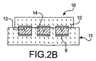
Surface Activated Bonding”)プラズマによる表面活性化のおかげで、ここでは、雰囲気温度でのシールを行うことができる。
埋設された軟質バンプは、例えば、パッシベーション層(あるいは、不動態化層)内に形成されたキャビティの底部のところにおける電解成長によって、形成することができる。パッシベーション層は、SiO2 から形成することができる。また、バンプは、インジウムまたはアルミニウムから形成することができる。
−複数のパッド22が既に形成されている基板21上においてパッシベーション層20(例えば、SiO2 )を成膜するというステップ、および、その後に、化学的エッチングを行うというステップ(図3A)と、
−Tiからなる連続的ベース層23を成膜するというステップ(図3B)と、
−樹脂からなるマスク25を成膜するというステップと、
−例えばインジウム24をあるいは他の任意の軟質導電性材料を電解成長させるというステップ(図3C)と、
−連続的ベース層と樹脂とを選択的に化学的エッチングするというステップ(図3D)と、
を行う。
一連をなす複数のポイントは、様々な手法によって形成することができる。例えば、金属の成膜や、エッチングや、電解成長や、電界成膜(『無電極』)プロセスや、金属のナノプリントや、互いに位置合わせされた複数のカーボンナノチューブの成長、等といったような様々な手法によって形成することができる。
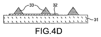
第1の技術においては、樹脂キャビティ上においてスパッタリングを行うことによって、金属の成膜体を形成する。成膜が進行するにつれて、開口が閉塞していき、キャビティの底部上へと成膜される金属の量が減少する。よって、キャビティの底部上において得られる形状は、円錐となる。
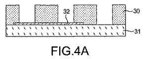
−複数のパッド32が既に形成されている基板31上において『リフトオフ』によって樹脂マスク30を成膜するというステップ(図4A)と、
−金属33を成膜するというステップ(図4Bおよび図4C)と、
−樹脂を除去するというステップ(図4D)と、
を行う。
また、傾斜側面を有した樹脂キャビティの底部において、金属の電解成長を行うことができる。そのような傾斜は、例えば、二重の樹脂コーティングによって、得ることができる。その場合、照射に対して互いに異なる感度を有した2種類の樹脂を、成膜する。照射後には、それら樹脂は、互いに異なる態様で溶解する。
−複数のパッド43が既に形成されている基板42上において2つの樹脂40,41を成膜することによって、二重樹脂コーティングを形成するというステップ(図5A)と、
−マスク45を介して紫外線44を照射するというステップ(図5B)と、
−照射を受けた樹脂部分を希薄するというステップ(図5C)と、
−ポイントを形成する材料46の電解成膜を行うというステップ(図5D)と、
−2つの樹脂40,41を除去するというステップ(図5E)と、
を行う。
また、本発明において独創的な手法として、ナノプリント技術を使用することによって、ポリマーを成型することができる。また、合金を融点付近へと加熱することによって、合金を成型することもできる。低い融点を有した合金を選択する必要がある。
−従来的手法によって合金層52が既に成膜されている基板51上において、モールド50をスタンピング形成するというステップ(図6Aおよび図6B)と、
−モールドを除去するというステップ(図6Cおよび図6D)と、
を行う。
電界の作用下においてナノチューブを成長させることができ、これにより、ナノチューブを配向させることができる。この技術は、上記の非特許文献1に記載されている。この非特許文献1においては、化学気相蒸着を使用することによって、フレキシブルなプラスチック基板上において鉛直方向に向き揃えされた複数のカーボンナノチューブからなるネットワークを直接的に成長させることを想定している。
−複数のパッド64が既に形成されている基板63上において、TiN層60と、Ni層61と、触媒層62と、を成膜するというステップ(図7A)と、
−触媒を液滴の態様とし、450℃においてナノチューブ65を成長させるというステップ(図7B)と、
を行う。
9 第2パッド
10 第1素子
11 第2素子
13 硬質導電性ポイント
14 軟質導電性バンプ
Claims (10)
- 第1素子(10)上に配置された一連をなす複数の第1パッド(8)と、第2素子(11)上に配置された一連をなす複数の第2埋設パッド(9)と、の間において電気的な接続を形成するための方法であって、
−前記第1素子(10)上の前記複数の第1パッド(8)の上に、一連をなす複数の硬質導電性ポイント(13)を形成し、
−前記第2素子(11)上の前記複数の第2埋設パッド(8)のところに、一連をなす複数の軟質導電性埋設バンプ(14)を形成し、
−前記ポイントと前記バンプとを、互いに対向させて配置し、
−前記第1素子を前記第2素子上に直接的に移送し、その際、前記ポイント(13)を前記バンプ(14)内へと侵入させるとともに、前記2つの素子の間における機械的な保持を、前記2つの素子の間において、前記バンプの間にわたっての直接的な接着によって確保することを特徴とする方法。 - 請求項1記載の方法において、
前記接着を、プラズマ活性化を使用して雰囲気温度において実行された分子接着によるシールとすることを特徴とする方法。 - 請求項1記載の方法において、
前記埋設バンプ(24)を、パッシベーション層(20)内に形成されたキャビティの底部のところにおける電解成長によって形成することを特徴とする方法。 - 請求項3記載の方法において、
−複数のパッド(22)が既に形成されている基板(21)上においてパッシベーション層(20)を成膜するというステップ、および、その後に、化学的エッチングを行うというステップと、
−導電性材料からなる連続的ベース層(23)を成膜するというステップと、
−マスク(25)を成膜するというステップと、
−軟質材料(24)を電解成長させて前記埋設バンプを形成するというステップと、
−選択的な化学的エッチングを行って前記マスクおよび前記連続的ベース層を除去するというステップと、
を行うことを特徴とする方法。 - 請求項1記載の方法において、
前記ポイントを、金属の成膜によって、または、エッチングによって、または、電解成長によって、または、金属のナノプリントによって、または、複数のナノチューブの互いに位置合わせされた成長によって、形成することを特徴とする方法。 - 第1素子(10)と、第2素子(11)と、の間において電気的な接続が形成されてなる素子であって、
前記第1素子(10)上には、一連をなす複数の第1パッド(8)が配置され、これら第1パッド(8)の上に、一連をなす複数の硬質導電性ポイント(13)が配置され、
前記第2素子(11)上には、一連をなす複数の第2埋設パッド(9)が配置され、これら第2埋設パッド(8)のところに、一連をなす複数の軟質導電性埋設バンプ(14)が配置され、
前記ポイント(13)が前記バンプ(14)内へと侵入しており、これにより、前記第1素子(10)と前記第2素子(11)との間において、前記第1パッド(8)と前記第2埋設パッド(9)との間の電気的な接続が形成され、
前記第1素子と前記第2素子との間の機械的な保持が、前記2つの素子の間において、前記バンプの間にわたっての直接的な接着によって確保されていることを特徴とする素子。 - 請求項6記載の素子において、
前記複数のポイントの全部が、または、前記複数のポイントの一部が、導電性材料から形成されていることを特徴とする素子。 - 請求項6記載の素子において、
前記ポイントが、ナノチューブまたはナノワイヤから形成されていることを特徴とする素子。 - 請求項6記載の素子において、
前記バンプが、少なくとも1つの導電性材料から形成されていることを特徴とする素子。 - 請求項9記載の素子において、
前記バンプの形成材料が、半田付けペーストまたは導電性接着剤とされていることを特徴とする素子。
Applications Claiming Priority (3)
| Application Number | Priority Date | Filing Date | Title |
|---|---|---|---|
| FR0452249 | 2004-10-04 | ||
| FR0452249A FR2876243B1 (fr) | 2004-10-04 | 2004-10-04 | Composant a protuberances conductrices ductiles enterrees et procede de connexion electrique entre ce composant et un composant muni de pointes conductrices dures |
| PCT/FR2005/050795 WO2006054005A1 (fr) | 2004-10-04 | 2005-09-29 | Composant a protuberances conductrices ductiles enterrees et procede de connexion electrique entre ce composant et un composant muni de pointes conductrices dures |
Publications (2)
| Publication Number | Publication Date |
|---|---|
| JP2008516424A JP2008516424A (ja) | 2008-05-15 |
| JP5583324B2 true JP5583324B2 (ja) | 2014-09-03 |
Family
ID=34982532
Family Applications (1)
| Application Number | Title | Priority Date | Filing Date |
|---|---|---|---|
| JP2007534065A Expired - Fee Related JP5583324B2 (ja) | 2004-10-04 | 2005-09-29 | 埋設された複数の軟質導電性バンプを備えた素子、ならびに、そのような素子と、複数の硬質導電性ポイントを備えた素子と、の電気的接続方法 |
Country Status (5)
| Country | Link |
|---|---|
| US (1) | US8586409B2 (ja) |
| EP (1) | EP1797748B1 (ja) |
| JP (1) | JP5583324B2 (ja) |
| FR (1) | FR2876243B1 (ja) |
| WO (1) | WO2006054005A1 (ja) |
Families Citing this family (19)
| Publication number | Priority date | Publication date | Assignee | Title |
|---|---|---|---|---|
| DE102006054468A1 (de) * | 2006-11-18 | 2008-05-29 | Braun Gmbh | Vorrichtung zur Entfernung von Körperhaar |
| TWI320680B (en) * | 2007-03-07 | 2010-02-11 | Phoenix Prec Technology Corp | Circuit board structure and fabrication method thereof |
| US7749887B2 (en) | 2007-12-18 | 2010-07-06 | Micron Technology, Inc. | Methods of fluxless micro-piercing of solder balls, and resulting devices |
| WO2009101664A1 (ja) * | 2008-02-15 | 2009-08-20 | Fujitsu Limited | 半導体装置の製造方法 |
| FR2928032B1 (fr) * | 2008-02-22 | 2011-06-17 | Commissariat Energie Atomique | Composant de connexion muni d'inserts avec cales compensatrices. |
| FR2928033B1 (fr) | 2008-02-22 | 2010-07-30 | Commissariat Energie Atomique | Composant de connexion muni d'inserts creux. |
| FR2936359B1 (fr) | 2008-09-25 | 2010-10-22 | Commissariat Energie Atomique | Connexion par emboitement de deux inserts soudes. |
| FR2938701A1 (fr) | 2008-11-20 | 2010-05-21 | Commissariat Energie Atomique | Procede d'amincissement d'un bloc reporte sur un substrat |
| KR101022912B1 (ko) * | 2008-11-28 | 2011-03-17 | 삼성전기주식회사 | 금속범프를 갖는 인쇄회로기판 및 그 제조방법 |
| FR2949172B1 (fr) | 2009-08-13 | 2011-08-26 | Commissariat Energie Atomique | Assemblage hermetique de deux composants et procede de realisation d'un tel assemblage |
| FR2949171B1 (fr) * | 2009-08-13 | 2011-08-26 | Commissariat Energie Atomique | Procede d'assemblage de deux composants electroniques |
| FR2964786B1 (fr) * | 2010-09-09 | 2013-03-15 | Commissariat Energie Atomique | Procédé de réalisation d'éléments a puce munis de rainures d'insertion de fils |
| FR2994331B1 (fr) | 2012-07-31 | 2014-09-12 | Commissariat Energie Atomique | Procede d'assemblage de deux composants electroniques entre eux, de type flip-chip |
| FR2996053A1 (fr) | 2012-09-27 | 2014-03-28 | Commissariat Energie Atomique | Procede d'assemblage de deux composants electroniques, de type flip-chip, assemblage obtenu selon le procede. |
| FR3055166B1 (fr) * | 2016-08-18 | 2020-12-25 | Commissariat Energie Atomique | Procede de connection intercomposants a densite optimisee |
| FR3082663B1 (fr) | 2018-06-14 | 2022-01-07 | Aledia | Dispositif optoelectronique |
| FR3082998B1 (fr) | 2018-06-25 | 2021-01-08 | Commissariat Energie Atomique | Dispositif et procedes pour le report de puces d'un substrat source vers un substrat destination |
| FR3091411B1 (fr) | 2018-12-28 | 2021-01-29 | Commissariat Energie Atomique | Procédés de fabrication optimisés d’une structure destinée à être assemblée par hybridation et d’un dispositif comprenant une telle structure |
| US10989735B2 (en) | 2019-08-21 | 2021-04-27 | Facebook Technologies, Llc | Atomic force microscopy tips for interconnection |
Family Cites Families (13)
| Publication number | Priority date | Publication date | Assignee | Title |
|---|---|---|---|---|
| US6414506B2 (en) * | 1993-09-03 | 2002-07-02 | Micron Technology, Inc. | Interconnect for testing semiconductor dice having raised bond pads |
| US6179198B1 (en) * | 1996-09-18 | 2001-01-30 | Matsushita Electric Industrial Co., Ltd. | Method of soldering bumped work by partially penetrating the oxide film covering the solder bumps |
| US5929521A (en) * | 1997-03-26 | 1999-07-27 | Micron Technology, Inc. | Projected contact structure for bumped semiconductor device and resulting articles and assemblies |
| JP2000150701A (ja) * | 1998-11-05 | 2000-05-30 | Shinko Electric Ind Co Ltd | 半導体装置並びにこれに用いる接続用基板及びその製造方法 |
| JP2000208675A (ja) * | 1999-01-11 | 2000-07-28 | Matsushita Electronics Industry Corp | 半導体装置およびその製造方法 |
| JP2001257453A (ja) * | 2000-03-09 | 2001-09-21 | Shinko Electric Ind Co Ltd | 配線基板、半導体装置及びそれらの製造方法 |
| US6362087B1 (en) * | 2000-05-05 | 2002-03-26 | Aptos Corporation | Method for fabricating a microelectronic fabrication having formed therein a redistribution structure |
| US6884313B2 (en) * | 2001-01-08 | 2005-04-26 | Fujitsu Limited | Method and system for joining and an ultra-high density interconnect |
| JP2002313995A (ja) * | 2001-04-19 | 2002-10-25 | Mitsubishi Electric Corp | ランドグリッドアレイ型半導体装置およびその実装方法 |
| US6387747B1 (en) * | 2001-05-31 | 2002-05-14 | Chartered Semiconductor Manufacturing Ltd. | Method to fabricate RF inductors with minimum area |
| JP3829325B2 (ja) * | 2002-02-07 | 2006-10-04 | 日本電気株式会社 | 半導体素子およびその製造方法並びに半導体装置の製造方法 |
| US7078822B2 (en) * | 2002-06-25 | 2006-07-18 | Intel Corporation | Microelectronic device interconnects |
| US20040198082A1 (en) * | 2003-04-07 | 2004-10-07 | Victor Zaderej | Method of making an electrical connector |
-
2004
- 2004-10-04 FR FR0452249A patent/FR2876243B1/fr not_active Expired - Lifetime
-
2005
- 2005-09-29 WO PCT/FR2005/050795 patent/WO2006054005A1/fr not_active Ceased
- 2005-09-29 JP JP2007534065A patent/JP5583324B2/ja not_active Expired - Fee Related
- 2005-09-29 EP EP05802576.8A patent/EP1797748B1/fr not_active Expired - Lifetime
- 2005-09-29 US US11/662,940 patent/US8586409B2/en not_active Expired - Fee Related
Also Published As
| Publication number | Publication date |
|---|---|
| WO2006054005A1 (fr) | 2006-05-26 |
| FR2876243B1 (fr) | 2007-01-26 |
| EP1797748A1 (fr) | 2007-06-20 |
| EP1797748B1 (fr) | 2017-05-17 |
| US8586409B2 (en) | 2013-11-19 |
| JP2008516424A (ja) | 2008-05-15 |
| US20080190655A1 (en) | 2008-08-14 |
| FR2876243A1 (fr) | 2006-04-07 |
Similar Documents
| Publication | Publication Date | Title |
|---|---|---|
| JP2008516424A (ja) | 埋設された複数の軟質導電性バンプを備えた素子、ならびに、そのような素子と、複数の硬質導電性ポイントを備えた素子と、の電気的接続方法 | |
| TWI398508B (zh) | 片狀結構及製造片狀結構之方法 | |
| JP4907539B2 (ja) | 複数の硬質導電性マイクロチップからなるアセンブリを備えた素子、ならびに、そのような素子と、軟質導電性突起を備えた素子と、の電気的接続方法 | |
| JP5585634B2 (ja) | 電子部品とその製造方法 | |
| CN1711210A (zh) | 集成结构及其制造方法 | |
| JP5378585B2 (ja) | 半導体装置 | |
| JP2004228135A (ja) | 微細孔への金属埋め込み方法 | |
| WO2015097878A1 (ja) | シート状構造体、これを用いた電子機器、シート状構造体の製造方法、及び電子機器の製造方法 | |
| US7239027B2 (en) | Bonding structure of device packaging | |
| JP2025068057A (ja) | 基板、積層構造、及び積層構造の製造方法 | |
| JP5319910B2 (ja) | 導電性パターンの埋設形成方法、積層基板の製造方法及び微細流路構造体の製造方法 | |
| CN102820269B (zh) | 半导体装置及其制造方法 | |
| JP5768786B2 (ja) | シート状構造体及び電子機器 | |
| CN115735270A (zh) | 基板键合方法 | |
| JPH10112474A (ja) | 半導体装置、半導体装置の製造方法、接点の形成方法、および電子装置の製造方法 | |
| JP2007516595A (ja) | 基板上に異方的導電性フィルムを形成するための方法 | |
| CN102361013B (zh) | 一种适用于晶圆级倒装芯片的金凸点制作方法 | |
| CN118633173A (zh) | 目标载体,半导体装置和用于转移半导体器件的方法和保持结构 | |
| KR101103275B1 (ko) | 반도체 소자 3차원 패키지용 관통 전극의 제조방법 | |
| Corsat et al. | Imprint technologies on conductive polymers and metals for interconnection and bumping purposes | |
| TW201140780A (en) | Packaging substrate structures and fabrication methods thereof | |
| JP2014197627A (ja) | 半導体パッケージ基板およびその製造方法 |
Legal Events
| Date | Code | Title | Description |
|---|---|---|---|
| A621 | Written request for application examination |
Free format text: JAPANESE INTERMEDIATE CODE: A621 Effective date: 20080922 |
|
| A977 | Report on retrieval |
Free format text: JAPANESE INTERMEDIATE CODE: A971007 Effective date: 20110726 |
|
| A131 | Notification of reasons for refusal |
Free format text: JAPANESE INTERMEDIATE CODE: A131 Effective date: 20110802 |
|
| A601 | Written request for extension of time |
Free format text: JAPANESE INTERMEDIATE CODE: A601 Effective date: 20111102 |
|
| A602 | Written permission of extension of time |
Free format text: JAPANESE INTERMEDIATE CODE: A602 Effective date: 20111110 |
|
| A601 | Written request for extension of time |
Free format text: JAPANESE INTERMEDIATE CODE: A601 Effective date: 20111201 |
|
| A602 | Written permission of extension of time |
Free format text: JAPANESE INTERMEDIATE CODE: A602 Effective date: 20111208 |
|
| A601 | Written request for extension of time |
Free format text: JAPANESE INTERMEDIATE CODE: A601 Effective date: 20111221 |
|
| A602 | Written permission of extension of time |
Free format text: JAPANESE INTERMEDIATE CODE: A602 Effective date: 20120104 |
|
| A521 | Request for written amendment filed |
Free format text: JAPANESE INTERMEDIATE CODE: A523 Effective date: 20120119 |
|
| A131 | Notification of reasons for refusal |
Free format text: JAPANESE INTERMEDIATE CODE: A131 Effective date: 20121016 |
|
| A601 | Written request for extension of time |
Free format text: JAPANESE INTERMEDIATE CODE: A601 Effective date: 20130116 |
|
| A602 | Written permission of extension of time |
Free format text: JAPANESE INTERMEDIATE CODE: A602 Effective date: 20130123 |
|
| A601 | Written request for extension of time |
Free format text: JAPANESE INTERMEDIATE CODE: A601 Effective date: 20130212 |
|
| A602 | Written permission of extension of time |
Free format text: JAPANESE INTERMEDIATE CODE: A602 Effective date: 20130219 |
|
| A601 | Written request for extension of time |
Free format text: JAPANESE INTERMEDIATE CODE: A601 Effective date: 20130306 |
|
| A602 | Written permission of extension of time |
Free format text: JAPANESE INTERMEDIATE CODE: A602 Effective date: 20130313 |
|
| A521 | Request for written amendment filed |
Free format text: JAPANESE INTERMEDIATE CODE: A523 Effective date: 20130416 |
|
| A02 | Decision of refusal |
Free format text: JAPANESE INTERMEDIATE CODE: A02 Effective date: 20140114 |
|
| A521 | Request for written amendment filed |
Free format text: JAPANESE INTERMEDIATE CODE: A523 Effective date: 20140514 |
|
| A911 | Transfer to examiner for re-examination before appeal (zenchi) |
Free format text: JAPANESE INTERMEDIATE CODE: A911 Effective date: 20140521 |
|
| TRDD | Decision of grant or rejection written | ||
| A01 | Written decision to grant a patent or to grant a registration (utility model) |
Free format text: JAPANESE INTERMEDIATE CODE: A01 Effective date: 20140616 |
|
| A61 | First payment of annual fees (during grant procedure) |
Free format text: JAPANESE INTERMEDIATE CODE: A61 Effective date: 20140716 |
|
| R150 | Certificate of patent or registration of utility model |
Ref document number: 5583324 Country of ref document: JP Free format text: JAPANESE INTERMEDIATE CODE: R150 |
|
| R250 | Receipt of annual fees |
Free format text: JAPANESE INTERMEDIATE CODE: R250 |
|
| R250 | Receipt of annual fees |
Free format text: JAPANESE INTERMEDIATE CODE: R250 |
|
| LAPS | Cancellation because of no payment of annual fees |