JP5584616B2 - 光出力デバイス - Google Patents
光出力デバイス Download PDFInfo
- Publication number
- JP5584616B2 JP5584616B2 JP2010510930A JP2010510930A JP5584616B2 JP 5584616 B2 JP5584616 B2 JP 5584616B2 JP 2010510930 A JP2010510930 A JP 2010510930A JP 2010510930 A JP2010510930 A JP 2010510930A JP 5584616 B2 JP5584616 B2 JP 5584616B2
- Authority
- JP
- Japan
- Prior art keywords
- light
- resin layer
- output device
- conductive layer
- layer
- Prior art date
- Legal status (The legal status is an assumption and is not a legal conclusion. Google has not performed a legal analysis and makes no representation as to the accuracy of the status listed.)
- Active
Links
Images




Classifications
-
- B—PERFORMING OPERATIONS; TRANSPORTING
- B32—LAYERED PRODUCTS
- B32B—LAYERED PRODUCTS, i.e. PRODUCTS BUILT-UP OF STRATA OF FLAT OR NON-FLAT, e.g. CELLULAR OR HONEYCOMB, FORM
- B32B17/00—Layered products essentially comprising sheet glass, or glass, slag, or like fibres
- B32B17/06—Layered products essentially comprising sheet glass, or glass, slag, or like fibres comprising glass as the main or only constituent of a layer, next to another layer of a specific material
- B32B17/10—Layered products essentially comprising sheet glass, or glass, slag, or like fibres comprising glass as the main or only constituent of a layer, next to another layer of a specific material of synthetic resin
- B32B17/10005—Layered products essentially comprising sheet glass, or glass, slag, or like fibres comprising glass as the main or only constituent of a layer, next to another layer of a specific material of synthetic resin laminated safety glass or glazing
- B32B17/10009—Layered products essentially comprising sheet glass, or glass, slag, or like fibres comprising glass as the main or only constituent of a layer, next to another layer of a specific material of synthetic resin laminated safety glass or glazing characterized by the number, the constitution or treatment of glass sheets
- B32B17/10036—Layered products essentially comprising sheet glass, or glass, slag, or like fibres comprising glass as the main or only constituent of a layer, next to another layer of a specific material of synthetic resin laminated safety glass or glazing characterized by the number, the constitution or treatment of glass sheets comprising two outer glass sheets
-
- B—PERFORMING OPERATIONS; TRANSPORTING
- B32—LAYERED PRODUCTS
- B32B—LAYERED PRODUCTS, i.e. PRODUCTS BUILT-UP OF STRATA OF FLAT OR NON-FLAT, e.g. CELLULAR OR HONEYCOMB, FORM
- B32B17/00—Layered products essentially comprising sheet glass, or glass, slag, or like fibres
- B32B17/06—Layered products essentially comprising sheet glass, or glass, slag, or like fibres comprising glass as the main or only constituent of a layer, next to another layer of a specific material
- B32B17/10—Layered products essentially comprising sheet glass, or glass, slag, or like fibres comprising glass as the main or only constituent of a layer, next to another layer of a specific material of synthetic resin
- B32B17/10005—Layered products essentially comprising sheet glass, or glass, slag, or like fibres comprising glass as the main or only constituent of a layer, next to another layer of a specific material of synthetic resin laminated safety glass or glazing
- B32B17/10165—Functional features of the laminated safety glass or glazing
- B32B17/10174—Coatings of a metallic or dielectric material on a constituent layer of glass or polymer
-
- B—PERFORMING OPERATIONS; TRANSPORTING
- B32—LAYERED PRODUCTS
- B32B—LAYERED PRODUCTS, i.e. PRODUCTS BUILT-UP OF STRATA OF FLAT OR NON-FLAT, e.g. CELLULAR OR HONEYCOMB, FORM
- B32B17/00—Layered products essentially comprising sheet glass, or glass, slag, or like fibres
- B32B17/06—Layered products essentially comprising sheet glass, or glass, slag, or like fibres comprising glass as the main or only constituent of a layer, next to another layer of a specific material
- B32B17/10—Layered products essentially comprising sheet glass, or glass, slag, or like fibres comprising glass as the main or only constituent of a layer, next to another layer of a specific material of synthetic resin
- B32B17/10005—Layered products essentially comprising sheet glass, or glass, slag, or like fibres comprising glass as the main or only constituent of a layer, next to another layer of a specific material of synthetic resin laminated safety glass or glazing
- B32B17/10165—Functional features of the laminated safety glass or glazing
- B32B17/10541—Functional features of the laminated safety glass or glazing comprising a light source or a light guide
-
- B—PERFORMING OPERATIONS; TRANSPORTING
- B32—LAYERED PRODUCTS
- B32B—LAYERED PRODUCTS, i.e. PRODUCTS BUILT-UP OF STRATA OF FLAT OR NON-FLAT, e.g. CELLULAR OR HONEYCOMB, FORM
- B32B17/00—Layered products essentially comprising sheet glass, or glass, slag, or like fibres
- B32B17/06—Layered products essentially comprising sheet glass, or glass, slag, or like fibres comprising glass as the main or only constituent of a layer, next to another layer of a specific material
- B32B17/10—Layered products essentially comprising sheet glass, or glass, slag, or like fibres comprising glass as the main or only constituent of a layer, next to another layer of a specific material of synthetic resin
- B32B17/10005—Layered products essentially comprising sheet glass, or glass, slag, or like fibres comprising glass as the main or only constituent of a layer, next to another layer of a specific material of synthetic resin laminated safety glass or glazing
- B32B17/1055—Layered products essentially comprising sheet glass, or glass, slag, or like fibres comprising glass as the main or only constituent of a layer, next to another layer of a specific material of synthetic resin laminated safety glass or glazing characterized by the resin layer, i.e. interlayer
- B32B17/10761—Layered products essentially comprising sheet glass, or glass, slag, or like fibres comprising glass as the main or only constituent of a layer, next to another layer of a specific material of synthetic resin laminated safety glass or glazing characterized by the resin layer, i.e. interlayer containing vinyl acetal
-
- B—PERFORMING OPERATIONS; TRANSPORTING
- B32—LAYERED PRODUCTS
- B32B—LAYERED PRODUCTS, i.e. PRODUCTS BUILT-UP OF STRATA OF FLAT OR NON-FLAT, e.g. CELLULAR OR HONEYCOMB, FORM
- B32B2307/00—Properties of the layers or laminate
- B32B2307/30—Properties of the layers or laminate having particular thermal properties
- B32B2307/302—Conductive
-
- F—MECHANICAL ENGINEERING; LIGHTING; HEATING; WEAPONS; BLASTING
- F21—LIGHTING
- F21K—NON-ELECTRIC LIGHT SOURCES USING LUMINESCENCE; LIGHT SOURCES USING ELECTROCHEMILUMINESCENCE; LIGHT SOURCES USING CHARGES OF COMBUSTIBLE MATERIAL; LIGHT SOURCES USING SEMICONDUCTOR DEVICES AS LIGHT-GENERATING ELEMENTS; LIGHT SOURCES NOT OTHERWISE PROVIDED FOR
- F21K9/00—Light sources using semiconductor devices as light-generating elements, e.g. using light-emitting diodes [LED] or lasers
-
- H—ELECTRICITY
- H10—SEMICONDUCTOR DEVICES; ELECTRIC SOLID-STATE DEVICES NOT OTHERWISE PROVIDED FOR
- H10W—GENERIC PACKAGES, INTERCONNECTIONS, CONNECTORS OR OTHER CONSTRUCTIONAL DETAILS OF DEVICES COVERED BY CLASS H10
- H10W90/00—Package configurations
-
- Y—GENERAL TAGGING OF NEW TECHNOLOGICAL DEVELOPMENTS; GENERAL TAGGING OF CROSS-SECTIONAL TECHNOLOGIES SPANNING OVER SEVERAL SECTIONS OF THE IPC; TECHNICAL SUBJECTS COVERED BY FORMER USPC CROSS-REFERENCE ART COLLECTIONS [XRACs] AND DIGESTS
- Y10—TECHNICAL SUBJECTS COVERED BY FORMER USPC
- Y10S—TECHNICAL SUBJECTS COVERED BY FORMER USPC CROSS-REFERENCE ART COLLECTIONS [XRACs] AND DIGESTS
- Y10S362/00—Illumination
- Y10S362/80—Light emitting diode
Landscapes
- Led Device Packages (AREA)
- Electroluminescent Light Sources (AREA)
- Arrangement Of Elements, Cooling, Sealing, Or The Like Of Lighting Devices (AREA)
- Laminated Bodies (AREA)
Description
少なくとも一つの光伝達基板と;
前記少なくとも一つの光源デバイスと熱的に接触する熱絶縁層と;
前記少なくとも一つの光源デバイスを熱的に接触する熱伝導層と;
を有する光出力デバイスが提供される。
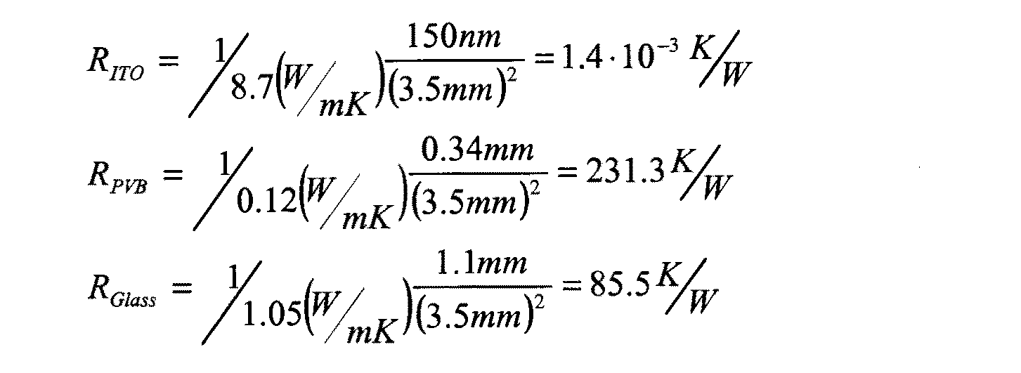
(i) PVBによる横方向の熱伝導。
(ii) PVBから上部のガラス板に流れる熱伝導。
(iii) ITO層、および底部のガラス板による熱伝導。“底部”のガラス板は、LEDがマウントされる板(すなわち、図3のガラス板1)として定義される。
q=単位時間あたりの熱伝導(W)
A=熱伝導の面積(m2)
k=熱伝導率(W/m.K または W/m.℃)
s=対象の厚さ(m)
この式を使用することにより、3つの熱伝導パスは以下のように表現することが可能である。
(i) PVBによる横方向の熱伝導。
Claims (13)
- 少なくとも一つの光源デバイスと;
第1及び第2の光透過性の基板と;
前記少なくとも一つの光源デバイスと熱的に接触する熱可塑性樹脂層又はレジン層であって、前記熱可塑性樹脂層又はレジン層は第1及び第2の光透過性の基板の間に位置する、熱可塑性樹脂層又はレジン層と;
前記少なくとも一つの光源デバイスと熱的に接触する、前記熱可塑性樹脂層又はレジン層並びに前記第1及び第2の光透過性の基板より熱伝導率の高い第1の熱伝導層と;
を有し、
前記第1の熱伝導層は、前記第1及び第2の光透過性の基板の一方の上に設けられ、かつ前記熱可塑性樹脂層又はレジン層並びに第1及び第2の前記光透過性の基板より熱伝導率の高い第2の熱伝導層は、前記第1及び第2の光透過性の基板の他方の上であって、かつ前記熱可塑性樹脂層又はレジン層と前記第1及び第2の光透過性の基板の他方との間に設けられている光出力デバイス。 - 前記熱可塑性樹脂層又はレジン層は、1W/mK未満の熱伝導率を有する、請求項1記載の光出力デバイス。
- 前記熱可塑性樹脂層又はレジン層は、0.2W/mK未満の熱伝導率である、請求項2記載の光出力デバイス。
- 前記第1の熱伝導層及び第2の熱伝導層は、それが設けられる前記第1及び第2の光透過性の基板の熱抵抗の10%未満の熱抵抗を有する、請求項1ないし3のうちいずれか1項に記載の光出力デバイス。
- 前記第1の熱伝導層及び第2の熱伝導層は、8.5K/W未満の熱抵抗を有する、請求項1ないし4のうちいずれか1項に記載の光出力デバイス。
- 前記第1の熱伝導層及び第2の熱伝導層は、W/Kを単位にして、K×d>0.002を満たす厚みd、および熱伝導率Kを有し、×は乗算を意味する、請求項1ないし5のうちいずれか1項に記載の光出力デバイス。
- 前記第1の熱伝導層及び第2の熱伝導層は、透明である、請求項1ないし6のうちいずれか1項に記載の光出力デバイス。
- 前記第1の熱伝導層及び第2の熱伝導層は、ダイヤモンドライクカーボン、MgO、およびSi3N4のうちの一つ以上を有する、請求項1ないし7のうちいずれか1項に記載の光出力デバイス。
- 前記第1および第2の光透過性の基板にはさまれる電極配置を更に有し、
前記少なくとも一つの光源デバイスは、前記電極配置へ接続されている、
請求項1ないし8のうちいずれか1項に記載の光出力デバイス。 - 前記電極配置は、実質的に透明な酸化インジウムスズ、酸化インジウム亜鉛、酸化スズまたはフッ素ドープ酸化スズを有する、請求項9記載の光出力デバイス。
- 1つの前記光源デバイス又は複数の前記光源デバイスは、無機LED、有機LED、高分子LED、またはレーザダイオードを有する、請求項1ないし10のうちいずれか1項に記載の光出力デバイス。
- 前記第1の熱伝導層及び第2の熱伝導層はパターン化され、かつ前記パターンは、1つの前記光源デバイス又は複数の前記光源デバイスの近傍または周辺の、少なくとも1つの領域または複数の領域を有する、請求項1ないし11のうちいずれか1項に記載の光出力デバイス。
- 請求項1ないし12のうちいずれか1項に記載の光出力デバイス、および前記光源デバイスに与えられる信号を制御するためのコントローラを有する、照明システム。
Applications Claiming Priority (3)
| Application Number | Priority Date | Filing Date | Title |
|---|---|---|---|
| EP07109836 | 2007-06-08 | ||
| EP07109836.2 | 2007-06-08 | ||
| PCT/IB2008/052137 WO2008149276A1 (en) | 2007-06-08 | 2008-06-02 | Light output device |
Publications (2)
| Publication Number | Publication Date |
|---|---|
| JP2010529669A JP2010529669A (ja) | 2010-08-26 |
| JP5584616B2 true JP5584616B2 (ja) | 2014-09-03 |
Family
ID=39743050
Family Applications (1)
| Application Number | Title | Priority Date | Filing Date |
|---|---|---|---|
| JP2010510930A Active JP5584616B2 (ja) | 2007-06-08 | 2008-06-02 | 光出力デバイス |
Country Status (6)
| Country | Link |
|---|---|
| US (1) | US8093789B2 (ja) |
| EP (1) | EP2158079B1 (ja) |
| JP (1) | JP5584616B2 (ja) |
| CN (1) | CN101689558B (ja) |
| TW (1) | TW200918804A (ja) |
| WO (1) | WO2008149276A1 (ja) |
Families Citing this family (39)
| Publication number | Priority date | Publication date | Assignee | Title |
|---|---|---|---|---|
| US8748922B2 (en) * | 2007-09-04 | 2014-06-10 | Koninklijke Philips N.V. | Light output device |
| US8372726B2 (en) | 2008-10-07 | 2013-02-12 | Mc10, Inc. | Methods and applications of non-planar imaging arrays |
| US8389862B2 (en) | 2008-10-07 | 2013-03-05 | Mc10, Inc. | Extremely stretchable electronics |
| US9123614B2 (en) | 2008-10-07 | 2015-09-01 | Mc10, Inc. | Methods and applications of non-planar imaging arrays |
| US8097926B2 (en) | 2008-10-07 | 2012-01-17 | Mc10, Inc. | Systems, methods, and devices having stretchable integrated circuitry for sensing and delivering therapy |
| US9289132B2 (en) | 2008-10-07 | 2016-03-22 | Mc10, Inc. | Catheter balloon having stretchable integrated circuitry and sensor array |
| US8886334B2 (en) | 2008-10-07 | 2014-11-11 | Mc10, Inc. | Systems, methods, and devices using stretchable or flexible electronics for medical applications |
| EP2422593A2 (en) * | 2009-04-23 | 2012-02-29 | AGC Glass Europe | Electronic structure |
| TWI592996B (zh) | 2009-05-12 | 2017-07-21 | 美國伊利諾大學理事會 | 用於可變形及半透明顯示器之超薄微刻度無機發光二極體之印刷總成 |
| US9723122B2 (en) | 2009-10-01 | 2017-08-01 | Mc10, Inc. | Protective cases with integrated electronics |
| US8666471B2 (en) | 2010-03-17 | 2014-03-04 | The Board Of Trustees Of The University Of Illinois | Implantable biomedical devices on bioresorbable substrates |
| US9936574B2 (en) | 2009-12-16 | 2018-04-03 | The Board Of Trustees Of The University Of Illinois | Waterproof stretchable optoelectronics |
| CN102884641B (zh) | 2010-03-16 | 2016-07-06 | 皇家飞利浦电子股份有限公司 | 具有可切换的照明/反射的光伏电池装置 |
| CN201829524U (zh) * | 2010-05-28 | 2011-05-11 | 景德镇正宇奈米科技有限公司 | 具有热辐射散热层的发光二极管 |
| US8698161B2 (en) * | 2010-12-17 | 2014-04-15 | Raytheon Company | Semiconductor structures having directly bonded diamond heat sinks and methods for making such structures |
| WO2012158709A1 (en) * | 2011-05-16 | 2012-11-22 | The Board Of Trustees Of The University Of Illinois | Thermally managed led arrays assembled by printing |
| US9159635B2 (en) | 2011-05-27 | 2015-10-13 | Mc10, Inc. | Flexible electronic structure |
| WO2013016652A1 (en) * | 2011-07-27 | 2013-01-31 | Grote Industries, Llc | Lighting device utilizing light active sheet material with integrated light emitting diode, disposed in seam and/or in low profile application |
| US20120175667A1 (en) * | 2011-10-03 | 2012-07-12 | Golle Aaron J | Led light disposed on a flexible substrate and connected with a printed 3d conductor |
| CN108389893A (zh) | 2011-12-01 | 2018-08-10 | 伊利诺伊大学评议会 | 经设计以经历可编程转变的瞬态器件 |
| US9696012B2 (en) * | 2012-10-04 | 2017-07-04 | Guardian Industries Corp. | Embedded LED assembly with optional beam steering optical element, and associated products, and/or methods |
| US9171794B2 (en) | 2012-10-09 | 2015-10-27 | Mc10, Inc. | Embedding thin chips in polymer |
| US10295124B2 (en) * | 2013-02-27 | 2019-05-21 | Cree, Inc. | Light emitter packages and methods |
| CN108922959B (zh) * | 2013-03-28 | 2022-07-29 | 日亚化学工业株式会社 | 发光装置、及使用发光装置的装置 |
| TWI512235B (zh) * | 2013-07-08 | 2015-12-11 | 雷盟光電股份有限公司 | 發光裝置 |
| US9698134B2 (en) * | 2014-11-27 | 2017-07-04 | Sct Technology, Ltd. | Method for manufacturing a light emitted diode display |
| US10925543B2 (en) | 2015-11-11 | 2021-02-23 | The Board Of Trustees Of The University Of Illinois | Bioresorbable silicon electronics for transient implants |
| US9997399B2 (en) * | 2016-08-16 | 2018-06-12 | Mikro Mesa Technology Co., Ltd. | Method for transferring semiconductor structure |
| WO2018043763A1 (en) | 2016-09-02 | 2018-03-08 | Kyushu University, National University Corporation | Continuous-wave organic thin-film distributed feedback laser and electrically driven organic semiconductor laser diode |
| TWI843470B (zh) | 2017-02-07 | 2024-05-21 | 國立大學法人九州大學 | 電流注入有機半導體雷射二極體及製造其之方法與程式 |
| GB2565041B (en) * | 2017-06-19 | 2021-12-29 | Liddle Richard | Transparent structure with electrically conductive elements |
| US20210028399A1 (en) * | 2018-03-30 | 2021-01-28 | Sharp Kabushiki Kaisha | Display device |
| US11917858B2 (en) * | 2018-09-06 | 2024-02-27 | Sharp Kabushiki Kaisha | Display device including molybdenum and polyphenylenew sulfide containing thermal insulation layer |
| DE112020005209T5 (de) | 2019-10-29 | 2022-12-29 | Osram Opto Semiconductors Gmbh | Optoelektronische Vorrichtung |
| US12040317B2 (en) | 2019-12-06 | 2024-07-16 | Osram Opto Semiconductors Gmbh | Optoelectronic device |
| US12328983B2 (en) | 2019-12-06 | 2025-06-10 | Osram Opto Semiconductors Gmbh | Optoelectronic arrangement |
| US12291096B2 (en) | 2019-12-06 | 2025-05-06 | Osram Opto Semiconductors Gmbh | Window or surface of a vehicle comprising at least one optoelectronic component |
| DE112020005977T5 (de) | 2019-12-06 | 2022-09-22 | Osram Opto Semiconductors Gmbh | Vorrichtung umfassend einen träger mit optoelektronischen elementen und verfahren zur herstellung der vorrichtung |
| WO2021110333A1 (en) * | 2019-12-06 | 2021-06-10 | Osram Opto Semiconductors Gmbh | Optoelectronic device |
Family Cites Families (19)
| Publication number | Priority date | Publication date | Assignee | Title |
|---|---|---|---|---|
| US5218351A (en) | 1987-01-12 | 1993-06-08 | Sekisui Kagaku Kogyo Kabushiki Kaisha | Electrically conductive transparent material and display device using the electrically conductive transparent material |
| DE19931689A1 (de) * | 1999-07-08 | 2001-01-11 | Patent Treuhand Ges Fuer Elektrische Gluehlampen Mbh | Optoelektronische Bauteilgruppe |
| US6867542B1 (en) * | 2000-03-29 | 2005-03-15 | General Electric Company | Floating chip photonic device and method of manufacture |
| JP2003131588A (ja) * | 2001-10-23 | 2003-05-09 | Matsushita Electric Ind Co Ltd | エレクトロルミネッセンス表示装置及びその製造方法 |
| US7043881B2 (en) | 2002-06-14 | 2006-05-16 | Tem-Pace, Inc. | Insulated glass assembly with an internal lighting system |
| BE1015302A3 (fr) * | 2003-01-10 | 2005-01-11 | Glaverbel | Vitrage comportant des composants electroniques. |
| US7049745B2 (en) * | 2003-11-25 | 2006-05-23 | Eastman Kodak Company | OLED display having thermally conductive layer |
| US20050225222A1 (en) * | 2004-04-09 | 2005-10-13 | Joseph Mazzochette | Light emitting diode arrays with improved light extraction |
| US7205717B2 (en) * | 2004-06-24 | 2007-04-17 | Eastman Kodak Company | OLED display having thermally conductive material |
| US7583022B2 (en) * | 2004-08-02 | 2009-09-01 | Eastman Kodak Company | OLED display with electrode |
| US7575354B2 (en) | 2004-09-16 | 2009-08-18 | Magna International Inc. | Thermal management system for solid state automotive lighting |
| TWI285969B (en) | 2005-06-22 | 2007-08-21 | Epistar Corp | Light emitting diode and method of the same |
| US7196354B1 (en) | 2005-09-29 | 2007-03-27 | Luminus Devices, Inc. | Wavelength-converting light-emitting devices |
| JP4950999B2 (ja) * | 2005-10-07 | 2012-06-13 | オスラム シルヴェニア インコーポレイテッド | 透光性のヒートシンクを有するled |
| FR2892594B1 (fr) * | 2005-10-21 | 2007-12-07 | Saint Gobain | Structure lumineuse comportant au moins une diode electroluminescente, sa fabrication et ses applications |
| JP2009516926A (ja) * | 2005-11-21 | 2009-04-23 | エージーシー フラット グラス ユーロップ エスエー | ガラス製品 |
| WO2007071724A1 (fr) | 2005-12-20 | 2007-06-28 | Agc Flat Glass Europe Sa | Moyen d'eclairage a diodes electroluminescentes |
| EP1834551B1 (fr) * | 2006-03-13 | 2008-05-14 | AGC Flat Glass Europe SA | Miroir éclairant |
| EP1886804A1 (fr) | 2006-08-02 | 2008-02-13 | AGC Flat Glass Europe SA | Eclairage au moyen de LEDs |
-
2008
- 2008-06-02 WO PCT/IB2008/052137 patent/WO2008149276A1/en not_active Ceased
- 2008-06-02 EP EP08751324.8A patent/EP2158079B1/en active Active
- 2008-06-02 US US12/602,684 patent/US8093789B2/en active Active
- 2008-06-02 CN CN2008800192682A patent/CN101689558B/zh active Active
- 2008-06-02 JP JP2010510930A patent/JP5584616B2/ja active Active
- 2008-06-05 TW TW097120968A patent/TW200918804A/zh unknown
Also Published As
| Publication number | Publication date |
|---|---|
| CN101689558A (zh) | 2010-03-31 |
| TW200918804A (en) | 2009-05-01 |
| JP2010529669A (ja) | 2010-08-26 |
| EP2158079A1 (en) | 2010-03-03 |
| WO2008149276A1 (en) | 2008-12-11 |
| EP2158079B1 (en) | 2018-05-02 |
| CN101689558B (zh) | 2012-07-18 |
| US20100176705A1 (en) | 2010-07-15 |
| US8093789B2 (en) | 2012-01-10 |
Similar Documents
| Publication | Publication Date | Title |
|---|---|---|
| JP5584616B2 (ja) | 光出力デバイス | |
| CN101687393B (zh) | 光输出装置 | |
| KR101759583B1 (ko) | 저항성 상호 접속층을 갖는 세그먼트 전계 발광 소자 | |
| KR20100058472A (ko) | 유기 기능 장치 및 그 제조 방법 | |
| CN101657672A (zh) | 光输出器件 | |
| TW201002140A (en) | Modular OLED device | |
| CN102365770A (zh) | 电致发光装置和分段照明装置 | |
| JP2017058635A (ja) | 融雪機能付led情報表示パネル及びled情報表示装置 | |
| CN100388092C (zh) | 背光模块的散热结构 | |
| US9615417B2 (en) | Dual polarity LED lighting device | |
| EP2095434B1 (en) | Led-based lighting device on a transparent substrate | |
| TWI769090B (zh) | 光源模組 | |
| TWI543039B (zh) | 平面加熱器 | |
| CN217216942U (zh) | 可发热的调光玻璃 | |
| US20250089132A1 (en) | Electric heating film | |
| TW510061B (en) | Layout structure of the electrode pin of organic light emitting diode | |
| CN111312886A (zh) | 发光二极管组件 | |
| TWI461104B (zh) | 有機電致發光元件 | |
| US7436669B2 (en) | 3D multi-layer heat conduction diffusion plate | |
| CN100462814C (zh) | 光源模块 | |
| JP2011187217A (ja) | 有機elモジュール | |
| CN117812968A (zh) | 一种oled基板、显示屏及电子设备 | |
| TWM649078U (zh) | 薄膜電熱片 | |
| JP4838618B2 (ja) | 液晶表示装置用パネルヒータ | |
| WO2010085748A2 (en) | Combined serial/parallel led configuration and single layer pcb containing the same |
Legal Events
| Date | Code | Title | Description |
|---|---|---|---|
| A621 | Written request for application examination |
Free format text: JAPANESE INTERMEDIATE CODE: A621 Effective date: 20110601 |
|
| A977 | Report on retrieval |
Free format text: JAPANESE INTERMEDIATE CODE: A971007 Effective date: 20121026 |
|
| A131 | Notification of reasons for refusal |
Free format text: JAPANESE INTERMEDIATE CODE: A131 Effective date: 20121106 |
|
| A521 | Request for written amendment filed |
Free format text: JAPANESE INTERMEDIATE CODE: A523 Effective date: 20130206 |
|
| A02 | Decision of refusal |
Free format text: JAPANESE INTERMEDIATE CODE: A02 Effective date: 20130319 |
|
| A521 | Request for written amendment filed |
Free format text: JAPANESE INTERMEDIATE CODE: A523 Effective date: 20130719 |
|
| A911 | Transfer to examiner for re-examination before appeal (zenchi) |
Free format text: JAPANESE INTERMEDIATE CODE: A911 Effective date: 20130726 |
|
| A912 | Re-examination (zenchi) completed and case transferred to appeal board |
Free format text: JAPANESE INTERMEDIATE CODE: A912 Effective date: 20130809 |
|
| A521 | Request for written amendment filed |
Free format text: JAPANESE INTERMEDIATE CODE: A523 Effective date: 20140528 |
|
| A61 | First payment of annual fees (during grant procedure) |
Free format text: JAPANESE INTERMEDIATE CODE: A61 Effective date: 20140718 |
|
| R150 | Certificate of patent or registration of utility model |
Ref document number: 5584616 Country of ref document: JP Free format text: JAPANESE INTERMEDIATE CODE: R150 |
|
| S111 | Request for change of ownership or part of ownership |
Free format text: JAPANESE INTERMEDIATE CODE: R313113 |
|
| R350 | Written notification of registration of transfer |
Free format text: JAPANESE INTERMEDIATE CODE: R350 |
|
| R250 | Receipt of annual fees |
Free format text: JAPANESE INTERMEDIATE CODE: R250 |
|
| R250 | Receipt of annual fees |
Free format text: JAPANESE INTERMEDIATE CODE: R250 |
|
| R250 | Receipt of annual fees |
Free format text: JAPANESE INTERMEDIATE CODE: R250 |
|
| S531 | Written request for registration of change of domicile |
Free format text: JAPANESE INTERMEDIATE CODE: R313531 |
|
| S533 | Written request for registration of change of name |
Free format text: JAPANESE INTERMEDIATE CODE: R313533 |
|
| R350 | Written notification of registration of transfer |
Free format text: JAPANESE INTERMEDIATE CODE: R350 |
|
| R250 | Receipt of annual fees |
Free format text: JAPANESE INTERMEDIATE CODE: R250 |
|
| R250 | Receipt of annual fees |
Free format text: JAPANESE INTERMEDIATE CODE: R250 |
|
| R250 | Receipt of annual fees |
Free format text: JAPANESE INTERMEDIATE CODE: R250 |
|
| R250 | Receipt of annual fees |
Free format text: JAPANESE INTERMEDIATE CODE: R250 |
|
| R250 | Receipt of annual fees |
Free format text: JAPANESE INTERMEDIATE CODE: R250 |