JP5584672B2 - 液晶表示装置 - Google Patents
液晶表示装置 Download PDFInfo
- Publication number
- JP5584672B2 JP5584672B2 JP2011255737A JP2011255737A JP5584672B2 JP 5584672 B2 JP5584672 B2 JP 5584672B2 JP 2011255737 A JP2011255737 A JP 2011255737A JP 2011255737 A JP2011255737 A JP 2011255737A JP 5584672 B2 JP5584672 B2 JP 5584672B2
- Authority
- JP
- Japan
- Prior art keywords
- liquid crystal
- polarizing plate
- absorption axis
- polarizer
- display device
- Prior art date
- Legal status (The legal status is an assumption and is not a legal conclusion. Google has not performed a legal analysis and makes no representation as to the accuracy of the status listed.)
- Active
Links
Images


Classifications
-
- G—PHYSICS
- G02—OPTICS
- G02F—OPTICAL DEVICES OR ARRANGEMENTS FOR THE CONTROL OF LIGHT BY MODIFICATION OF THE OPTICAL PROPERTIES OF THE MEDIA OF THE ELEMENTS INVOLVED THEREIN; NON-LINEAR OPTICS; FREQUENCY-CHANGING OF LIGHT; OPTICAL LOGIC ELEMENTS; OPTICAL ANALOGUE/DIGITAL CONVERTERS
- G02F1/00—Devices or arrangements for the control of the intensity, colour, phase, polarisation or direction of light arriving from an independent light source, e.g. switching, gating or modulating; Non-linear optics
- G02F1/01—Devices or arrangements for the control of the intensity, colour, phase, polarisation or direction of light arriving from an independent light source, e.g. switching, gating or modulating; Non-linear optics for the control of the intensity, phase, polarisation or colour
- G02F1/13—Devices or arrangements for the control of the intensity, colour, phase, polarisation or direction of light arriving from an independent light source, e.g. switching, gating or modulating; Non-linear optics for the control of the intensity, phase, polarisation or colour based on liquid crystals, e.g. single liquid crystal display cells
- G02F1/133—Constructional arrangements; Operation of liquid crystal cells; Circuit arrangements
- G02F1/1333—Constructional arrangements; Manufacturing methods
- G02F1/1335—Structural association of cells with optical devices, e.g. polarisers or reflectors
- G02F1/133528—Polarisers
-
- G—PHYSICS
- G02—OPTICS
- G02F—OPTICAL DEVICES OR ARRANGEMENTS FOR THE CONTROL OF LIGHT BY MODIFICATION OF THE OPTICAL PROPERTIES OF THE MEDIA OF THE ELEMENTS INVOLVED THEREIN; NON-LINEAR OPTICS; FREQUENCY-CHANGING OF LIGHT; OPTICAL LOGIC ELEMENTS; OPTICAL ANALOGUE/DIGITAL CONVERTERS
- G02F1/00—Devices or arrangements for the control of the intensity, colour, phase, polarisation or direction of light arriving from an independent light source, e.g. switching, gating or modulating; Non-linear optics
- G02F1/01—Devices or arrangements for the control of the intensity, colour, phase, polarisation or direction of light arriving from an independent light source, e.g. switching, gating or modulating; Non-linear optics for the control of the intensity, phase, polarisation or colour
- G02F1/13—Devices or arrangements for the control of the intensity, colour, phase, polarisation or direction of light arriving from an independent light source, e.g. switching, gating or modulating; Non-linear optics for the control of the intensity, phase, polarisation or colour based on liquid crystals, e.g. single liquid crystal display cells
- G02F1/133—Constructional arrangements; Operation of liquid crystal cells; Circuit arrangements
- G02F1/1333—Constructional arrangements; Manufacturing methods
- G02F1/1335—Structural association of cells with optical devices, e.g. polarisers or reflectors
- G02F1/133528—Polarisers
- G02F1/133531—Polarisers characterised by the arrangement of polariser or analyser axes
-
- G—PHYSICS
- G02—OPTICS
- G02F—OPTICAL DEVICES OR ARRANGEMENTS FOR THE CONTROL OF LIGHT BY MODIFICATION OF THE OPTICAL PROPERTIES OF THE MEDIA OF THE ELEMENTS INVOLVED THEREIN; NON-LINEAR OPTICS; FREQUENCY-CHANGING OF LIGHT; OPTICAL LOGIC ELEMENTS; OPTICAL ANALOGUE/DIGITAL CONVERTERS
- G02F1/00—Devices or arrangements for the control of the intensity, colour, phase, polarisation or direction of light arriving from an independent light source, e.g. switching, gating or modulating; Non-linear optics
- G02F1/01—Devices or arrangements for the control of the intensity, colour, phase, polarisation or direction of light arriving from an independent light source, e.g. switching, gating or modulating; Non-linear optics for the control of the intensity, phase, polarisation or colour
- G02F1/13—Devices or arrangements for the control of the intensity, colour, phase, polarisation or direction of light arriving from an independent light source, e.g. switching, gating or modulating; Non-linear optics for the control of the intensity, phase, polarisation or colour based on liquid crystals, e.g. single liquid crystal display cells
- G02F1/133—Constructional arrangements; Operation of liquid crystal cells; Circuit arrangements
- G02F1/1333—Constructional arrangements; Manufacturing methods
- G02F1/1335—Structural association of cells with optical devices, e.g. polarisers or reflectors
- G02F1/13363—Birefringent elements, e.g. for optical compensation
-
- G—PHYSICS
- G02—OPTICS
- G02F—OPTICAL DEVICES OR ARRANGEMENTS FOR THE CONTROL OF LIGHT BY MODIFICATION OF THE OPTICAL PROPERTIES OF THE MEDIA OF THE ELEMENTS INVOLVED THEREIN; NON-LINEAR OPTICS; FREQUENCY-CHANGING OF LIGHT; OPTICAL LOGIC ELEMENTS; OPTICAL ANALOGUE/DIGITAL CONVERTERS
- G02F2201/00—Constructional arrangements not provided for in groups G02F1/00 - G02F7/00
- G02F2201/54—Arrangements for reducing warping-twist
-
- G—PHYSICS
- G02—OPTICS
- G02F—OPTICAL DEVICES OR ARRANGEMENTS FOR THE CONTROL OF LIGHT BY MODIFICATION OF THE OPTICAL PROPERTIES OF THE MEDIA OF THE ELEMENTS INVOLVED THEREIN; NON-LINEAR OPTICS; FREQUENCY-CHANGING OF LIGHT; OPTICAL LOGIC ELEMENTS; OPTICAL ANALOGUE/DIGITAL CONVERTERS
- G02F2202/00—Materials and properties
- G02F2202/28—Adhesive materials or arrangements
-
- G—PHYSICS
- G02—OPTICS
- G02F—OPTICAL DEVICES OR ARRANGEMENTS FOR THE CONTROL OF LIGHT BY MODIFICATION OF THE OPTICAL PROPERTIES OF THE MEDIA OF THE ELEMENTS INVOLVED THEREIN; NON-LINEAR OPTICS; FREQUENCY-CHANGING OF LIGHT; OPTICAL LOGIC ELEMENTS; OPTICAL ANALOGUE/DIGITAL CONVERTERS
- G02F2413/00—Indexing scheme related to G02F1/13363, i.e. to birefringent elements, e.g. for optical compensation, characterised by the number, position, orientation or value of the compensation plates
- G02F2413/02—Number of plates being 2
-
- G—PHYSICS
- G02—OPTICS
- G02F—OPTICAL DEVICES OR ARRANGEMENTS FOR THE CONTROL OF LIGHT BY MODIFICATION OF THE OPTICAL PROPERTIES OF THE MEDIA OF THE ELEMENTS INVOLVED THEREIN; NON-LINEAR OPTICS; FREQUENCY-CHANGING OF LIGHT; OPTICAL LOGIC ELEMENTS; OPTICAL ANALOGUE/DIGITAL CONVERTERS
- G02F2413/00—Indexing scheme related to G02F1/13363, i.e. to birefringent elements, e.g. for optical compensation, characterised by the number, position, orientation or value of the compensation plates
- G02F2413/08—Indexing scheme related to G02F1/13363, i.e. to birefringent elements, e.g. for optical compensation, characterised by the number, position, orientation or value of the compensation plates with a particular optical axis orientation
Landscapes
- Physics & Mathematics (AREA)
- Nonlinear Science (AREA)
- Mathematical Physics (AREA)
- Chemical & Material Sciences (AREA)
- Crystallography & Structural Chemistry (AREA)
- General Physics & Mathematics (AREA)
- Optics & Photonics (AREA)
- Liquid Crystal (AREA)
- Polarising Elements (AREA)
Description
Claims (6)
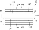
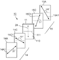
- 第2面側から入射し透過する光を制御して第1面側に出射し液晶層をガラス基板内に封入した四辺形の表示面を有する液晶セルと、吸収軸を有する偏光子を有し前記液晶セルの前記第1面側に粘着層により貼着された第1偏光板と、吸収軸を有する偏光子を有し前記液晶セルの前記第2面側に粘着層により貼着された第2偏光板とを具備する液晶表示装置において、前記第1偏光板と前記第2偏光板のうち、前記表示面において吸収軸方向の最大寸法が大きい偏光子を有する偏光板は、吸収軸方向の最大寸法が小さい偏光子を有する偏光板よりも、ガラス基板密着力の高い粘着層で貼着けられており、
前記第1偏光板の吸収軸方向は、前記表示面の各辺に対して平行ではなく垂直ではなく、
前記第2偏光板の吸収軸方向は、前記表示面の前記各辺に対して平行ではなく垂直ではないことを特徴とする液晶表示装置。 - 前記表示面において吸収軸方向の最大寸法が大きい偏光子を有する偏光板の前記粘着層は、前記吸収軸方向の最大寸法が小さい偏光子を有する偏光板の粘着層よりも、前記偏光子が収縮する温度範囲での密着力が高いことを特徴とする請求項1記載の液晶表示装置。
- 前記両偏光板の粘着層のうち少なくとも一方の粘着層が導電性あるいは帯電防止処理が施されている請求項1記載の液晶表示装置。
- 前記吸収軸方向の最大寸法が小さい偏光子を有する偏光板の前記粘着層が導電性あるいは帯電防止処理が施されている請求項3に記載の液晶表示装置。
- 前記液晶セルは前記液晶層を挟んで一対の電極が形成され、いずれか一方の電極に画素ごとに非導電スリットが形成されている請求項1記載の液晶表示装置。
- 前記第1偏光板の前記偏光子と前記液晶セルとの間および前記第2偏光板の前記偏光子と前記液晶セルとの間に位相差フィルムが配置され、かつ前記第1偏光板の前記偏光子の吸収軸と前記第2偏光板の前記偏光子の吸収軸が90度交差し前記位相差フィルムの各辺に対し平行または垂直でない配置とされていることを特徴とする請求項1記載の液晶表示装置。
Priority Applications (2)
| Application Number | Priority Date | Filing Date | Title |
|---|---|---|---|
| JP2011255737A JP5584672B2 (ja) | 2011-11-24 | 2011-11-24 | 液晶表示装置 |
| US13/684,348 US9019447B2 (en) | 2011-11-24 | 2012-11-23 | Liquid crystal display device with polarizing plates |
Applications Claiming Priority (1)
| Application Number | Priority Date | Filing Date | Title |
|---|---|---|---|
| JP2011255737A JP5584672B2 (ja) | 2011-11-24 | 2011-11-24 | 液晶表示装置 |
Publications (2)
| Publication Number | Publication Date |
|---|---|
| JP2013109250A JP2013109250A (ja) | 2013-06-06 |
| JP5584672B2 true JP5584672B2 (ja) | 2014-09-03 |
Family
ID=48466563
Family Applications (1)
| Application Number | Title | Priority Date | Filing Date |
|---|---|---|---|
| JP2011255737A Active JP5584672B2 (ja) | 2011-11-24 | 2011-11-24 | 液晶表示装置 |
Country Status (2)
| Country | Link |
|---|---|
| US (1) | US9019447B2 (ja) |
| JP (1) | JP5584672B2 (ja) |
Families Citing this family (7)
| Publication number | Priority date | Publication date | Assignee | Title |
|---|---|---|---|---|
| JP6214866B2 (ja) | 2012-10-31 | 2017-10-18 | 株式会社ジャパンディスプレイ | 液晶表示装置 |
| CN104122703B (zh) * | 2013-09-30 | 2017-03-22 | 深超光电(深圳)有限公司 | 液晶显示装置、其制作方法以及电子装置 |
| DE102013017627B4 (de) * | 2013-10-23 | 2020-03-12 | e.solutions GmbH | Polarisierender Mehrschichtenfilm und Verfahren zur Herstellung einer den Film umfassenden Vorrichtung |
| JP2016139027A (ja) * | 2015-01-28 | 2016-08-04 | 日東電工株式会社 | 偏光板および液晶表示装置 |
| JP2017026939A (ja) * | 2015-07-27 | 2017-02-02 | 日東電工株式会社 | 偏光板および液晶表示装置 |
| WO2017026079A1 (ja) * | 2015-08-07 | 2017-02-16 | 住友化学株式会社 | 偏光板及び画像表示装置 |
| JP2017097087A (ja) * | 2015-11-20 | 2017-06-01 | 住友化学株式会社 | 偏光板及び画像表示装置 |
Family Cites Families (10)
| Publication number | Priority date | Publication date | Assignee | Title |
|---|---|---|---|---|
| JPH08160223A (ja) * | 1994-12-08 | 1996-06-21 | Sekisui Chem Co Ltd | 粘着剤層付き偏光板 |
| JP2005115056A (ja) * | 2003-10-08 | 2005-04-28 | Toshiba Matsushita Display Technology Co Ltd | 液晶表示装置及び液晶表示装置の製造方法 |
| WO2006001527A1 (en) * | 2004-06-29 | 2006-01-05 | Fujifilm Corporation | Optical cellulose acylate film, polarizing plate and liquid crystal display |
| KR100692695B1 (ko) * | 2004-11-30 | 2007-03-14 | 비오이 하이디스 테크놀로지 주식회사 | 액정표시장치 |
| US7541074B2 (en) * | 2005-08-17 | 2009-06-02 | Fujifilm Corporation | Optical film and optical compensatory film, polarizing plate and liquid crystal display using same |
| JP2007279323A (ja) | 2006-04-05 | 2007-10-25 | Toshiba Matsushita Display Technology Co Ltd | 液晶表示装置 |
| JP5073427B2 (ja) * | 2007-09-11 | 2012-11-14 | 日東電工株式会社 | 液晶パネル、及び液晶表示装置 |
| KR101161600B1 (ko) * | 2007-10-22 | 2012-07-03 | 가부시키가이샤 닛폰 쇼쿠바이 | 편광판, 그 제조 방법, 광학 필름 및 화상 표시 장치 |
| US8174648B2 (en) * | 2009-07-29 | 2012-05-08 | Fujifilm Corporation | Cellulose acylate film, process for producing the same, and polarizing plate and liquid crystal display device having the same |
| JP5251827B2 (ja) * | 2009-10-26 | 2013-07-31 | 住友化学株式会社 | 液晶表示装置 |
-
2011
- 2011-11-24 JP JP2011255737A patent/JP5584672B2/ja active Active
-
2012
- 2012-11-23 US US13/684,348 patent/US9019447B2/en active Active
Also Published As
| Publication number | Publication date |
|---|---|
| US20130135564A1 (en) | 2013-05-30 |
| US9019447B2 (en) | 2015-04-28 |
| JP2013109250A (ja) | 2013-06-06 |
Similar Documents
| Publication | Publication Date | Title |
|---|---|---|
| JP6820417B2 (ja) | 表示装置 | |
| JP5584672B2 (ja) | 液晶表示装置 | |
| CN103913887B (zh) | 具有宽视角的液晶显示装置 | |
| CN103869401B (zh) | 偏振板及其制备方法和包括它的液晶显示器 | |
| KR102177588B1 (ko) | 나노캡슐 액정층을 포함하는 액정표시장치 | |
| CN103018962B (zh) | 一种液晶显示屏及显示设备 | |
| WO2019103012A1 (ja) | 表示装置 | |
| CN106662776B (zh) | 液晶显示装置 | |
| JP2020529627A (ja) | 液晶表示装置およびその製造方法 | |
| JP6587685B2 (ja) | 液晶表示装置 | |
| CN102112910B (zh) | 垂直取向型液晶显示装置 | |
| US10809563B2 (en) | Liquid crystal display device | |
| CN102768380A (zh) | 一种偏光片、液晶显示屏和液晶显示装置 | |
| JP2019128430A (ja) | 液晶表示装置ならびに該液晶表示装置に用いられる光学部材および光学部材のセット | |
| JP2010015038A (ja) | 液晶表示装置 | |
| CN105988245B (zh) | 液晶面板和液晶显示装置 | |
| CN202677027U (zh) | 一种液晶面板以及显示装置 | |
| KR20180033225A (ko) | 터치 패널 부착 액정 표시 장치 | |
| US9684201B2 (en) | Liquid crystal display device | |
| KR20120120848A (ko) | 광 시야각을 갖는 수평 전계형 액정표시장치 | |
| JP2009003432A (ja) | 液晶表示装置 | |
| JP5475963B2 (ja) | 液晶表示装置 | |
| KR20160080497A (ko) | 빛샘이 방지된 곡면 액정표시장치 | |
| CN105785655A (zh) | 显示面板 | |
| JP2010191240A (ja) | 液晶表示装置 |
Legal Events
| Date | Code | Title | Description |
|---|---|---|---|
| A621 | Written request for application examination |
Free format text: JAPANESE INTERMEDIATE CODE: A621 Effective date: 20130325 |
|
| RD04 | Notification of resignation of power of attorney |
Free format text: JAPANESE INTERMEDIATE CODE: A7424 Effective date: 20130614 |
|
| RD04 | Notification of resignation of power of attorney |
Free format text: JAPANESE INTERMEDIATE CODE: A7424 Effective date: 20130624 |
|
| A711 | Notification of change in applicant |
Free format text: JAPANESE INTERMEDIATE CODE: A712 Effective date: 20130624 |
|
| RD03 | Notification of appointment of power of attorney |
Free format text: JAPANESE INTERMEDIATE CODE: A7423 Effective date: 20130909 |
|
| A977 | Report on retrieval |
Free format text: JAPANESE INTERMEDIATE CODE: A971007 Effective date: 20130911 |
|
| A131 | Notification of reasons for refusal |
Free format text: JAPANESE INTERMEDIATE CODE: A131 Effective date: 20131028 |
|
| A977 | Report on retrieval |
Free format text: JAPANESE INTERMEDIATE CODE: A971007 Effective date: 20131030 |
|
| A521 | Request for written amendment filed |
Free format text: JAPANESE INTERMEDIATE CODE: A523 Effective date: 20131216 |
|
| TRDD | Decision of grant or rejection written | ||
| A01 | Written decision to grant a patent or to grant a registration (utility model) |
Free format text: JAPANESE INTERMEDIATE CODE: A01 Effective date: 20140708 |
|
| A61 | First payment of annual fees (during grant procedure) |
Free format text: JAPANESE INTERMEDIATE CODE: A61 Effective date: 20140718 |
|
| R150 | Certificate of patent or registration of utility model |
Ref document number: 5584672 Country of ref document: JP Free format text: JAPANESE INTERMEDIATE CODE: R150 |
|
| R250 | Receipt of annual fees |
Free format text: JAPANESE INTERMEDIATE CODE: R250 |
|
| R250 | Receipt of annual fees |
Free format text: JAPANESE INTERMEDIATE CODE: R250 |
|
| R250 | Receipt of annual fees |
Free format text: JAPANESE INTERMEDIATE CODE: R250 |
|
| R250 | Receipt of annual fees |
Free format text: JAPANESE INTERMEDIATE CODE: R250 |
|
| R250 | Receipt of annual fees |
Free format text: JAPANESE INTERMEDIATE CODE: R250 |
|
| R250 | Receipt of annual fees |
Free format text: JAPANESE INTERMEDIATE CODE: R250 |
|
| R250 | Receipt of annual fees |
Free format text: JAPANESE INTERMEDIATE CODE: R250 |
|
| R250 | Receipt of annual fees |
Free format text: JAPANESE INTERMEDIATE CODE: R250 |
|
| R250 | Receipt of annual fees |
Free format text: JAPANESE INTERMEDIATE CODE: R250 |
|
| S111 | Request for change of ownership or part of ownership |
Free format text: JAPANESE INTERMEDIATE CODE: R313113 |
|
| R350 | Written notification of registration of transfer |
Free format text: JAPANESE INTERMEDIATE CODE: R350 |