JP5588035B2 - 印刷回路基板のパネル - Google Patents
印刷回路基板のパネル Download PDFInfo
- Publication number
- JP5588035B2 JP5588035B2 JP2013056944A JP2013056944A JP5588035B2 JP 5588035 B2 JP5588035 B2 JP 5588035B2 JP 2013056944 A JP2013056944 A JP 2013056944A JP 2013056944 A JP2013056944 A JP 2013056944A JP 5588035 B2 JP5588035 B2 JP 5588035B2
- Authority
- JP
- Japan
- Prior art keywords
- plating
- circuit board
- printed circuit
- metal layer
- lead
- Prior art date
- Legal status (The legal status is an assumption and is not a legal conclusion. Google has not performed a legal analysis and makes no representation as to the accuracy of the status listed.)
- Expired - Fee Related
Links
Images


Classifications
-
- H—ELECTRICITY
- H05—ELECTRIC TECHNIQUES NOT OTHERWISE PROVIDED FOR
- H05K—PRINTED CIRCUITS; CASINGS OR CONSTRUCTIONAL DETAILS OF ELECTRIC APPARATUS; MANUFACTURE OF ASSEMBLAGES OF ELECTRICAL COMPONENTS
- H05K1/00—Printed circuits
- H05K1/02—Details
-
- H—ELECTRICITY
- H05—ELECTRIC TECHNIQUES NOT OTHERWISE PROVIDED FOR
- H05K—PRINTED CIRCUITS; CASINGS OR CONSTRUCTIONAL DETAILS OF ELECTRIC APPARATUS; MANUFACTURE OF ASSEMBLAGES OF ELECTRICAL COMPONENTS
- H05K3/00—Apparatus or processes for manufacturing printed circuits
- H05K3/22—Secondary treatment of printed circuits
- H05K3/24—Reinforcing of the conductive pattern
- H05K3/241—Reinforcing of the conductive pattern characterised by the electroplating method; means therefor, e.g. baths or apparatus
- H05K3/242—Reinforcing of the conductive pattern characterised by the electroplating method; means therefor, e.g. baths or apparatus characterised by using temporary conductors on the printed circuit for electrically connecting areas which are to be electroplated
-
- H—ELECTRICITY
- H05—ELECTRIC TECHNIQUES NOT OTHERWISE PROVIDED FOR
- H05K—PRINTED CIRCUITS; CASINGS OR CONSTRUCTIONAL DETAILS OF ELECTRIC APPARATUS; MANUFACTURE OF ASSEMBLAGES OF ELECTRICAL COMPONENTS
- H05K3/00—Apparatus or processes for manufacturing printed circuits
- H05K3/10—Apparatus or processes for manufacturing printed circuits in which conductive material is applied to the insulating support in such a manner as to form the desired conductive pattern
- H05K3/18—Apparatus or processes for manufacturing printed circuits in which conductive material is applied to the insulating support in such a manner as to form the desired conductive pattern using precipitation techniques to apply the conductive material
-
- H—ELECTRICITY
- H10—SEMICONDUCTOR DEVICES; ELECTRIC SOLID-STATE DEVICES NOT OTHERWISE PROVIDED FOR
- H10W—GENERIC PACKAGES, INTERCONNECTIONS, CONNECTORS OR OTHER CONSTRUCTIONAL DETAILS OF DEVICES COVERED BY CLASS H10
- H10W70/00—Package substrates; Interposers; Redistribution layers [RDL]
- H10W70/60—Insulating or insulated package substrates; Interposers; Redistribution layers
- H10W70/62—Insulating or insulated package substrates; Interposers; Redistribution layers characterised by their interconnections
- H10W70/65—Shapes or dispositions of interconnections
-
- H—ELECTRICITY
- H05—ELECTRIC TECHNIQUES NOT OTHERWISE PROVIDED FOR
- H05K—PRINTED CIRCUITS; CASINGS OR CONSTRUCTIONAL DETAILS OF ELECTRIC APPARATUS; MANUFACTURE OF ASSEMBLAGES OF ELECTRICAL COMPONENTS
- H05K2201/00—Indexing scheme relating to printed circuits covered by H05K1/00
- H05K2201/09—Shape and layout
- H05K2201/09209—Shape and layout details of conductors
- H05K2201/09218—Conductive traces
- H05K2201/09263—Meander
-
- H—ELECTRICITY
- H05—ELECTRIC TECHNIQUES NOT OTHERWISE PROVIDED FOR
- H05K—PRINTED CIRCUITS; CASINGS OR CONSTRUCTIONAL DETAILS OF ELECTRIC APPARATUS; MANUFACTURE OF ASSEMBLAGES OF ELECTRICAL COMPONENTS
- H05K2203/00—Indexing scheme relating to apparatus or processes for manufacturing printed circuits covered by H05K3/00
- H05K2203/17—Post-manufacturing processes
- H05K2203/175—Configurations of connections suitable for easy deletion, e.g. modifiable circuits or temporary conductors for electroplating; Processes for deleting connections
-
- H—ELECTRICITY
- H05—ELECTRIC TECHNIQUES NOT OTHERWISE PROVIDED FOR
- H05K—PRINTED CIRCUITS; CASINGS OR CONSTRUCTIONAL DETAILS OF ELECTRIC APPARATUS; MANUFACTURE OF ASSEMBLAGES OF ELECTRICAL COMPONENTS
- H05K3/00—Apparatus or processes for manufacturing printed circuits
- H05K3/0011—Working of insulating substrates or insulating layers
- H05K3/0044—Mechanical working of the substrate, e.g. drilling or punching
- H05K3/0052—Depaneling, i.e. dividing a panel into circuit boards; Working of the edges of circuit boards
-
- H—ELECTRICITY
- H05—ELECTRIC TECHNIQUES NOT OTHERWISE PROVIDED FOR
- H05K—PRINTED CIRCUITS; CASINGS OR CONSTRUCTIONAL DETAILS OF ELECTRIC APPARATUS; MANUFACTURE OF ASSEMBLAGES OF ELECTRICAL COMPONENTS
- H05K3/00—Apparatus or processes for manufacturing printed circuits
- H05K3/22—Secondary treatment of printed circuits
- H05K3/28—Applying non-metallic protective coatings
- H05K3/284—Applying non-metallic protective coatings for encapsulating mounted components
Landscapes
- Engineering & Computer Science (AREA)
- Microelectronics & Electronic Packaging (AREA)
- Manufacturing & Machinery (AREA)
- Structure Of Printed Boards (AREA)
- Manufacturing Of Printed Wiring (AREA)
Description
上記リードラインは複数であってもよい。
なお、上記の発明の概要は、本発明の必要な特徴の全てを列挙したものではない。また、これらの特徴群のサブコンビネーションもまた、発明となりうる。
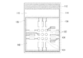
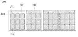
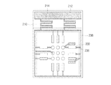
214 リードライン
236,238 メッキリード線
232 パッド
Claims (2)
- パッドが形成された複数の単位基板が設けられる基板ストリップ領域と、前記基板ストリップ領域にメッキを施すための電流が印加されるメッキリード線と、前記基板ストリップ領域の外郭に設けられるダミー領域とを含む薄型印刷回路基板のパネルであって、
前記ダミー領域に剛性を確保するための補強金属層が設けられ、
前記補強金属層の少なくとも一部が、移動時にクランピングのために露出され、
前記メッキリード線と前記補強金属層の露出された一部とが、複数個所折曲した形状のリードラインにより電気的に接続され、
前記メッキリード線は、前記パッドと接続され、前記メッキリード線に印加された電流の一部を前記パッドに伝達し、
前記リードラインは、前記メッキリード線に印加された電流の残りを前記補強金属層に伝達することを特徴とする印刷回路基板のパネル。 - 前記リードラインが複数であることを特徴とする請求項1に記載の印刷回路基板のパネ
ル。
Applications Claiming Priority (2)
| Application Number | Priority Date | Filing Date | Title |
|---|---|---|---|
| KR1020090081211A KR101066642B1 (ko) | 2009-08-31 | 2009-08-31 | 인쇄회로기판 제조방법 |
| KR10-2009-0081211 | 2009-08-31 |
Related Parent Applications (1)
| Application Number | Title | Priority Date | Filing Date |
|---|---|---|---|
| JP2010108483A Division JP5323763B2 (ja) | 2009-08-31 | 2010-05-10 | 印刷回路基板のストリップ及びパネル |
Publications (2)
| Publication Number | Publication Date |
|---|---|
| JP2013118418A JP2013118418A (ja) | 2013-06-13 |
| JP5588035B2 true JP5588035B2 (ja) | 2014-09-10 |
Family
ID=43623161
Family Applications (2)
| Application Number | Title | Priority Date | Filing Date |
|---|---|---|---|
| JP2010108483A Expired - Fee Related JP5323763B2 (ja) | 2009-08-31 | 2010-05-10 | 印刷回路基板のストリップ及びパネル |
| JP2013056944A Expired - Fee Related JP5588035B2 (ja) | 2009-08-31 | 2013-03-19 | 印刷回路基板のパネル |
Family Applications Before (1)
| Application Number | Title | Priority Date | Filing Date |
|---|---|---|---|
| JP2010108483A Expired - Fee Related JP5323763B2 (ja) | 2009-08-31 | 2010-05-10 | 印刷回路基板のストリップ及びパネル |
Country Status (5)
| Country | Link |
|---|---|
| US (1) | US8253032B2 (ja) |
| JP (2) | JP5323763B2 (ja) |
| KR (1) | KR101066642B1 (ja) |
| CN (1) | CN102005427B (ja) |
| TW (1) | TWI395526B (ja) |
Families Citing this family (6)
| Publication number | Priority date | Publication date | Assignee | Title |
|---|---|---|---|---|
| CN102376673A (zh) * | 2010-08-06 | 2012-03-14 | 南亚电路板股份有限公司 | 封装基板及其形成方法 |
| CN103046031B (zh) * | 2012-12-11 | 2014-08-13 | 胜宏科技(惠州)股份有限公司 | 一种线路板电镀金方法 |
| KR20140108865A (ko) | 2013-03-04 | 2014-09-15 | 삼성전자주식회사 | 패키지 기판, 패키지 기판의 제조 방법 및 패키지 기판을 포함하는 반도체 패키지 |
| KR102211089B1 (ko) * | 2014-05-23 | 2021-02-02 | 해성디에스 주식회사 | 반도체칩 실장용 인쇄회로기판 |
| JP7003012B2 (ja) * | 2018-08-10 | 2022-02-04 | 日東電工株式会社 | 配線回路基板集合体シートおよびその製造方法 |
| CN111668111B (zh) * | 2019-03-08 | 2021-09-21 | 矽磐微电子(重庆)有限公司 | 半导体封装方法 |
Family Cites Families (44)
| Publication number | Priority date | Publication date | Assignee | Title |
|---|---|---|---|---|
| JPS575394A (en) * | 1980-06-11 | 1982-01-12 | Fujitsu Ltd | Method of electrolytically plaing printed board contact plug terminal |
| US5956237A (en) * | 1993-12-24 | 1999-09-21 | Ibiden Co., Ltd. | Primary printed wiring board |
| JP3066251B2 (ja) * | 1994-08-05 | 2000-07-17 | シャープ株式会社 | プリント配線基板 |
| JP3680398B2 (ja) * | 1995-12-26 | 2005-08-10 | イビデン株式会社 | プリント配線板 |
| JPH11177191A (ja) * | 1997-12-12 | 1999-07-02 | Mitsubishi Electric Corp | プリント配線板および多層プリント配線板 |
| JP2997746B2 (ja) * | 1998-05-27 | 2000-01-11 | 亜南半導体株式会社 | 印刷回路基板 |
| US6278618B1 (en) * | 1999-07-23 | 2001-08-21 | National Semiconductor Corporation | Substrate strips for use in integrated circuit packaging |
| JP3427352B2 (ja) * | 1999-08-24 | 2003-07-14 | アムコー テクノロジー コリア インコーポレーティド | 半導体パッケージ用回路基板 |
| US6206694B1 (en) * | 1999-11-24 | 2001-03-27 | Crystalmark Dental Systems, Inc. | Handpiece assembly for air abrasion |
| US20010026537A1 (en) * | 2000-02-24 | 2001-10-04 | Michael Massey | Satellite internet backbone network system using virtual onboard switching |
| JP4246876B2 (ja) * | 2000-03-23 | 2009-04-02 | 日本特殊陶業株式会社 | 配線基板 |
| JP2002261426A (ja) * | 2001-02-28 | 2002-09-13 | Optrex Corp | フレキシブル配線基板 |
| WO2002080268A1 (en) | 2001-03-30 | 2002-10-10 | Infineon Technologies Ag | A substrate for mounting a semiconductor chip |
| US7443010B2 (en) * | 2001-04-05 | 2008-10-28 | Taiwan Semiconductor Manufacturing Co., Ltd. | Matrix form semiconductor package substrate having an electrode of serpentine shape |
| US7017042B1 (en) * | 2001-06-14 | 2006-03-21 | Syrus Ziai | Method and circuit to accelerate IPSec processing |
| KR100944695B1 (ko) * | 2001-06-27 | 2010-02-26 | 신꼬오덴기 고교 가부시키가이샤 | 위치 정보를 갖는 배선 기판 |
| JP2003086735A (ja) * | 2001-06-27 | 2003-03-20 | Shinko Electric Ind Co Ltd | 位置情報付配線基板及びその製造方法並びに半導体装置の製造方法 |
| JP4051273B2 (ja) * | 2002-08-30 | 2008-02-20 | 日本特殊陶業株式会社 | 配線基板及び配線基板の製造方法 |
| JP4451298B2 (ja) * | 2004-12-20 | 2010-04-14 | 大日本印刷株式会社 | Icカードモジュール体 |
| SG145564A1 (en) * | 2003-09-09 | 2008-09-29 | Micron Technology Inc | Systems for degating packaged semiconductor devices with tape substrates |
| JP2005209761A (ja) | 2004-01-21 | 2005-08-04 | Sumitomo Metal Electronics Devices Inc | 多数個取り配線基板 |
| US7181837B2 (en) * | 2004-06-04 | 2007-02-27 | Micron Technology, Inc. | Plating buss and a method of use thereof |
| US7643409B2 (en) * | 2004-08-25 | 2010-01-05 | Cisco Technology, Inc. | Computer network with point-to-point pseudowire redundancy |
| KR100845534B1 (ko) * | 2004-12-31 | 2008-07-10 | 엘지전자 주식회사 | 전도성 금속 도금 폴리이미드 기판 및 그 제조 방법 |
| US20060171369A1 (en) * | 2005-02-03 | 2006-08-03 | Telefonaktiebolaget L M Ericsson (Publ) | Resource utilization for multimedia broadcast multicast services (MBMS) |
| US8675486B2 (en) * | 2005-05-17 | 2014-03-18 | Hughes Network Systems, Llc | Method and system for efficient flow control in a spot beam satellite system |
| GB2428103B (en) * | 2005-07-07 | 2009-06-17 | Agilent Technologies Inc | An optical device |
| KR100693755B1 (ko) * | 2005-07-27 | 2007-03-12 | 앰코 테크놀로지 코리아 주식회사 | 반도체 패키지 제조용 리드프레임 구조 |
| US7684640B2 (en) * | 2005-10-20 | 2010-03-23 | Sharp Laboratories Of America, Inc. | Methods and systems for automatic digital image enhancement with local adjustment |
| JP4312758B2 (ja) * | 2005-12-27 | 2009-08-12 | 日本特殊陶業株式会社 | 配線基板の製造方法、配線基板の中間製品 |
| JP2007180211A (ja) * | 2005-12-27 | 2007-07-12 | Ngk Spark Plug Co Ltd | 配線基板製造用コア基板、配線基板の製造方法 |
| KR100797670B1 (ko) * | 2006-06-12 | 2008-01-23 | 삼성전기주식회사 | 인쇄회로기판의 도금선 형성 방법 |
| JP5037071B2 (ja) * | 2006-08-29 | 2012-09-26 | 新光電気工業株式会社 | 樹脂封止型半導体装置の製造方法 |
| US7701073B2 (en) * | 2006-09-19 | 2010-04-20 | Texas Instruments Incorporated | Locking feature and method for manufacturing transfer molded IC packages |
| US20090001573A1 (en) * | 2007-01-08 | 2009-01-01 | Phontara Jirawongsapiwat | Structure and method for wire bond integrity check on BGA substrates using indirect electrical interconnectivity pathway between wire bonds and ground |
| JP2009027009A (ja) * | 2007-07-20 | 2009-02-05 | Fujikura Ltd | フレキシブルプリント基板のメッキリード構造 |
| WO2009045299A1 (en) * | 2007-10-03 | 2009-04-09 | Virtela Communications, Inc. | Virtualized application acceleration infrastructure |
| KR100901512B1 (ko) * | 2007-10-30 | 2009-06-08 | 삼성전기주식회사 | 기판 스트립 |
| KR20090054817A (ko) * | 2007-11-27 | 2009-06-01 | 삼성전기주식회사 | 인쇄회로기판 |
| US8457035B2 (en) * | 2009-04-17 | 2013-06-04 | Viasat, Inc. | Mobility across satellite beams using L2 connectivity |
| US8427999B2 (en) * | 2009-04-17 | 2013-04-23 | Viasat, Inc. | Multi-satellite architecture |
| WO2010121220A1 (en) * | 2009-04-17 | 2010-10-21 | Viasat, Inc. | Packet acceleration through a network tunnel |
| US8804730B2 (en) * | 2009-04-17 | 2014-08-12 | Viasat, Inc. | Layer-2 extension services |
| US20100265927A1 (en) * | 2009-04-21 | 2010-10-21 | Crestcom, Inc. | Efficient Allocation of Power to Bandwidth In a Multi-Carrier Cellular Communication System |
-
2009
- 2009-08-31 KR KR1020090081211A patent/KR101066642B1/ko not_active Expired - Fee Related
-
2010
- 2010-04-16 US US12/761,828 patent/US8253032B2/en not_active Expired - Fee Related
- 2010-04-27 CN CN2010101595641A patent/CN102005427B/zh not_active Expired - Fee Related
- 2010-04-28 TW TW099113532A patent/TWI395526B/zh not_active IP Right Cessation
- 2010-05-10 JP JP2010108483A patent/JP5323763B2/ja not_active Expired - Fee Related
-
2013
- 2013-03-19 JP JP2013056944A patent/JP5588035B2/ja not_active Expired - Fee Related
Also Published As
| Publication number | Publication date |
|---|---|
| TWI395526B (zh) | 2013-05-01 |
| KR20110023373A (ko) | 2011-03-08 |
| JP5323763B2 (ja) | 2013-10-23 |
| TW201108896A (en) | 2011-03-01 |
| CN102005427A (zh) | 2011-04-06 |
| CN102005427B (zh) | 2012-09-19 |
| US20110048784A1 (en) | 2011-03-03 |
| KR101066642B1 (ko) | 2011-09-22 |
| JP2011054930A (ja) | 2011-03-17 |
| US8253032B2 (en) | 2012-08-28 |
| JP2013118418A (ja) | 2013-06-13 |
Similar Documents
| Publication | Publication Date | Title |
|---|---|---|
| KR100551641B1 (ko) | 반도체 장치의 제조 방법 및 반도체 장치 | |
| JP5588035B2 (ja) | 印刷回路基板のパネル | |
| JP2008263125A5 (ja) | ||
| KR20090054817A (ko) | 인쇄회로기판 | |
| CN101488463A (zh) | 半导体封装用基板的制造方法及利用它来制造的金属镀层 | |
| CN106358379A (zh) | 印刷电路板及其制造方法 | |
| US8952514B2 (en) | Semiconductor package | |
| CN104517929B (zh) | 封装载板 | |
| JP6109078B2 (ja) | リードクラックが強化された電子素子用テープ | |
| KR101167453B1 (ko) | 전자부품 내장형 인쇄회로기판 및 그 제조방법 | |
| US9318354B2 (en) | Semiconductor package and fabrication method thereof | |
| CN103715164B (zh) | 柔性电路板及芯片封装结构 | |
| US20070267759A1 (en) | Semiconductor device with a distributed plating pattern | |
| US20070269929A1 (en) | Method of reducing stress on a semiconductor die with a distributed plating pattern | |
| WO2015129185A1 (ja) | 樹脂封止型半導体装置、およびその製造方法、ならびにその実装体 | |
| JP5587464B2 (ja) | 半導体装置の製造方法 | |
| CN206282839U (zh) | 一种薄型阵列塑料封装件 | |
| CN205944063U (zh) | 封装基板 | |
| TW201203411A (en) | Manufacturing method of chip package and chip package manufactured using the same | |
| US20150342047A1 (en) | Circuit board, electronic component and method of manufacturing circuit board | |
| KR101008422B1 (ko) | 인쇄회로기판 제조방법 | |
| KR20110090023A (ko) | 무기판 반도체 칩 패키지 제조 방법 및 이를 이용하여 제조된 무기판 반도체 칩 패키지 | |
| KR20220001005A (ko) | 인쇄회로기관의 도금층 형성 방법 및 이에 의해 형성된 패키지용 인쇄회로기판 | |
| KR20090131776A (ko) | 다열형 리드리스 리드프레임 및 그의 반도체 패키지 및그의 제조방법 | |
| JP2014207471A (ja) | 半導体装置の製造方法 |
Legal Events
| Date | Code | Title | Description |
|---|---|---|---|
| A131 | Notification of reasons for refusal |
Free format text: JAPANESE INTERMEDIATE CODE: A131 Effective date: 20131112 |
|
| A521 | Request for written amendment filed |
Free format text: JAPANESE INTERMEDIATE CODE: A523 Effective date: 20140115 |
|
| TRDD | Decision of grant or rejection written | ||
| A01 | Written decision to grant a patent or to grant a registration (utility model) |
Free format text: JAPANESE INTERMEDIATE CODE: A01 Effective date: 20140624 |
|
| A61 | First payment of annual fees (during grant procedure) |
Free format text: JAPANESE INTERMEDIATE CODE: A61 Effective date: 20140724 |
|
| R150 | Certificate of patent or registration of utility model |
Ref document number: 5588035 Country of ref document: JP Free format text: JAPANESE INTERMEDIATE CODE: R150 |
|
| R250 | Receipt of annual fees |
Free format text: JAPANESE INTERMEDIATE CODE: R250 |
|
| R250 | Receipt of annual fees |
Free format text: JAPANESE INTERMEDIATE CODE: R250 |
|
| R250 | Receipt of annual fees |
Free format text: JAPANESE INTERMEDIATE CODE: R250 |
|
| R250 | Receipt of annual fees |
Free format text: JAPANESE INTERMEDIATE CODE: R250 |
|
| R250 | Receipt of annual fees |
Free format text: JAPANESE INTERMEDIATE CODE: R250 |
|
| R250 | Receipt of annual fees |
Free format text: JAPANESE INTERMEDIATE CODE: R250 |
|
| LAPS | Cancellation because of no payment of annual fees |