JP5634793B2 - 導波路、マイクロプリズムおよび微小機械光変調器を含むディスプレイ - Google Patents
導波路、マイクロプリズムおよび微小機械光変調器を含むディスプレイ Download PDFInfo
- Publication number
- JP5634793B2 JP5634793B2 JP2010180901A JP2010180901A JP5634793B2 JP 5634793 B2 JP5634793 B2 JP 5634793B2 JP 2010180901 A JP2010180901 A JP 2010180901A JP 2010180901 A JP2010180901 A JP 2010180901A JP 5634793 B2 JP5634793 B2 JP 5634793B2
- Authority
- JP
- Japan
- Prior art keywords
- light
- layer
- refractive index
- display
- optical waveguide
- Prior art date
- Legal status (The legal status is an assumption and is not a legal conclusion. Google has not performed a legal analysis and makes no representation as to the accuracy of the status listed.)
- Expired - Fee Related
Links
Images

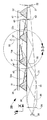
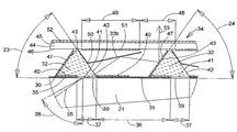


Classifications
-
- G—PHYSICS
- G02—OPTICS
- G02B—OPTICAL ELEMENTS, SYSTEMS OR APPARATUS
- G02B5/00—Optical elements other than lenses
- G02B5/04—Prisms
- G02B5/045—Prism arrays
-
- G—PHYSICS
- G02—OPTICS
- G02B—OPTICAL ELEMENTS, SYSTEMS OR APPARATUS
- G02B26/00—Optical devices or arrangements for the control of light using movable or deformable optical elements
- G02B26/08—Optical devices or arrangements for the control of light using movable or deformable optical elements for controlling the direction of light
- G02B26/0816—Optical devices or arrangements for the control of light using movable or deformable optical elements for controlling the direction of light by means of one or more reflecting elements
- G02B26/0833—Optical devices or arrangements for the control of light using movable or deformable optical elements for controlling the direction of light by means of one or more reflecting elements the reflecting element being a micromechanical device, e.g. a MEMS mirror, DMD
- G02B26/0841—Optical devices or arrangements for the control of light using movable or deformable optical elements for controlling the direction of light by means of one or more reflecting elements the reflecting element being a micromechanical device, e.g. a MEMS mirror, DMD the reflecting element being moved or deformed by electrostatic means
-
- G—PHYSICS
- G02—OPTICS
- G02B—OPTICAL ELEMENTS, SYSTEMS OR APPARATUS
- G02B6/00—Light guides; Structural details of arrangements comprising light guides and other optical elements, e.g. couplings
- G02B6/0001—Light guides; Structural details of arrangements comprising light guides and other optical elements, e.g. couplings specially adapted for lighting devices or systems
- G02B6/0011—Light guides; Structural details of arrangements comprising light guides and other optical elements, e.g. couplings specially adapted for lighting devices or systems the light guides being planar or of plate-like form
- G02B6/0033—Means for improving the coupling-out of light from the light guide
- G02B6/0035—Means for improving the coupling-out of light from the light guide provided on the surface of the light guide or in the bulk of it
- G02B6/0036—2-D arrangement of prisms, protrusions, indentations or roughened surfaces
-
- G—PHYSICS
- G02—OPTICS
- G02B—OPTICAL ELEMENTS, SYSTEMS OR APPARATUS
- G02B6/00—Light guides; Structural details of arrangements comprising light guides and other optical elements, e.g. couplings
- G02B6/0001—Light guides; Structural details of arrangements comprising light guides and other optical elements, e.g. couplings specially adapted for lighting devices or systems
- G02B6/0011—Light guides; Structural details of arrangements comprising light guides and other optical elements, e.g. couplings specially adapted for lighting devices or systems the light guides being planar or of plate-like form
- G02B6/0033—Means for improving the coupling-out of light from the light guide
- G02B6/0035—Means for improving the coupling-out of light from the light guide provided on the surface of the light guide or in the bulk of it
- G02B6/0038—Linear indentations or grooves, e.g. arc-shaped grooves or meandering grooves, extending over the full length or width of the light guide
-
- G—PHYSICS
- G02—OPTICS
- G02B—OPTICAL ELEMENTS, SYSTEMS OR APPARATUS
- G02B6/00—Light guides; Structural details of arrangements comprising light guides and other optical elements, e.g. couplings
- G02B6/0001—Light guides; Structural details of arrangements comprising light guides and other optical elements, e.g. couplings specially adapted for lighting devices or systems
- G02B6/0011—Light guides; Structural details of arrangements comprising light guides and other optical elements, e.g. couplings specially adapted for lighting devices or systems the light guides being planar or of plate-like form
- G02B6/0033—Means for improving the coupling-out of light from the light guide
- G02B6/0035—Means for improving the coupling-out of light from the light guide provided on the surface of the light guide or in the bulk of it
- G02B6/0045—Means for improving the coupling-out of light from the light guide provided on the surface of the light guide or in the bulk of it by shaping at least a portion of the light guide
- G02B6/0046—Tapered light guide, e.g. wedge-shaped light guide
-
- G—PHYSICS
- G09—EDUCATION; CRYPTOGRAPHY; DISPLAY; ADVERTISING; SEALS
- G09G—ARRANGEMENTS OR CIRCUITS FOR CONTROL OF INDICATING DEVICES USING STATIC MEANS TO PRESENT VARIABLE INFORMATION
- G09G3/00—Control arrangements or circuits, of interest only in connection with visual indicators other than cathode-ray tubes
- G09G3/20—Control arrangements or circuits, of interest only in connection with visual indicators other than cathode-ray tubes for presentation of an assembly of a number of characters, e.g. a page, by composing the assembly by combination of individual elements arranged in a matrix no fixed position being assigned to or needed to be assigned to the individual characters or partial characters
- G09G3/34—Control arrangements or circuits, of interest only in connection with visual indicators other than cathode-ray tubes for presentation of an assembly of a number of characters, e.g. a page, by composing the assembly by combination of individual elements arranged in a matrix no fixed position being assigned to or needed to be assigned to the individual characters or partial characters by control of light from an independent source
- G09G3/3433—Control arrangements or circuits, of interest only in connection with visual indicators other than cathode-ray tubes for presentation of an assembly of a number of characters, e.g. a page, by composing the assembly by combination of individual elements arranged in a matrix no fixed position being assigned to or needed to be assigned to the individual characters or partial characters by control of light from an independent source using light modulating elements actuated by an electric field and being other than liquid crystal devices and electrochromic devices
- G09G3/3473—Control arrangements or circuits, of interest only in connection with visual indicators other than cathode-ray tubes for presentation of an assembly of a number of characters, e.g. a page, by composing the assembly by combination of individual elements arranged in a matrix no fixed position being assigned to or needed to be assigned to the individual characters or partial characters by control of light from an independent source using light modulating elements actuated by an electric field and being other than liquid crystal devices and electrochromic devices based on light coupled out of a light guide, e.g. due to scattering, by contracting the light guide with external means
Landscapes
- Physics & Mathematics (AREA)
- General Physics & Mathematics (AREA)
- Optics & Photonics (AREA)
- Engineering & Computer Science (AREA)
- Nonlinear Science (AREA)
- Computer Hardware Design (AREA)
- Theoretical Computer Science (AREA)
- Mechanical Light Control Or Optical Switches (AREA)
- Mathematical Physics (AREA)
- Chemical & Material Sciences (AREA)
- Crystallography & Structural Chemistry (AREA)
- Micromachines (AREA)
Applications Claiming Priority (4)
| Application Number | Priority Date | Filing Date | Title |
|---|---|---|---|
| US12/583,156 US8177406B2 (en) | 2007-12-19 | 2009-08-13 | Display including waveguide, micro-prisms and micro-mirrors |
| US12/583,156 | 2009-08-13 | ||
| US12/802,037 US8313226B2 (en) | 2010-05-28 | 2010-05-28 | Display including waveguide, micro-prisms and micro-shutters |
| US12/802,037 | 2010-05-28 |
Publications (2)
| Publication Number | Publication Date |
|---|---|
| JP2011059679A JP2011059679A (ja) | 2011-03-24 |
| JP5634793B2 true JP5634793B2 (ja) | 2014-12-03 |
Family
ID=43302415
Family Applications (1)
| Application Number | Title | Priority Date | Filing Date |
|---|---|---|---|
| JP2010180901A Expired - Fee Related JP5634793B2 (ja) | 2009-08-13 | 2010-08-12 | 導波路、マイクロプリズムおよび微小機械光変調器を含むディスプレイ |
Country Status (4)
| Country | Link |
|---|---|
| EP (1) | EP2284594B1 (fr) |
| JP (1) | JP5634793B2 (fr) |
| KR (1) | KR101699291B1 (fr) |
| CN (1) | CN101995656B (fr) |
Families Citing this family (10)
| Publication number | Priority date | Publication date | Assignee | Title |
|---|---|---|---|---|
| CN103454847B (zh) * | 2012-05-29 | 2016-05-18 | 杨文君 | 平面波导显示器和系统 |
| CN107577040B (zh) * | 2016-07-04 | 2022-03-01 | 爱德华·帕克奇亚恩 | 用于mems显示器的光调制器 |
| CN107577042A (zh) * | 2016-07-04 | 2018-01-12 | 爱德华·帕克奇亚恩 | Mems显示器 |
| CN107577043B (zh) * | 2016-07-04 | 2021-10-08 | 爱德华·帕克奇亚恩 | 用于显示器的mems光调制器 |
| KR102590788B1 (ko) * | 2016-07-04 | 2023-10-17 | 에드워드 파크얀 | Mems 디스플레이 |
| CN107577041B (zh) * | 2016-07-04 | 2022-05-31 | 爱德华·帕克奇亚恩 | Mems显示器 |
| KR102712568B1 (ko) * | 2016-07-04 | 2024-09-30 | 에드워드 파크얀 | 디스플레이용 mems 광 변조기 |
| EP3622342A4 (fr) * | 2017-05-08 | 2021-02-17 | RealD Spark, LLC | Empilement optique pour affichage directionnel |
| CN110208896B (zh) * | 2019-05-21 | 2024-03-12 | 安徽省东超科技有限公司 | 一种新型光波导及应用新型光波导的屏幕 |
| CN116931336A (zh) * | 2022-04-12 | 2023-10-24 | 深圳市中光工业技术研究院 | 集成光学耦合开关 |
Family Cites Families (14)
| Publication number | Priority date | Publication date | Assignee | Title |
|---|---|---|---|---|
| US5428468A (en) * | 1993-11-05 | 1995-06-27 | Alliedsignal Inc. | Illumination system employing an array of microprisms |
| US5914760A (en) * | 1996-06-21 | 1999-06-22 | Casio Computer Co., Ltd. | Surface light source device and liquid crystal display device using the same |
| JP3787983B2 (ja) * | 1997-06-18 | 2006-06-21 | セイコーエプソン株式会社 | 光スイッチング素子、画像表示装置及び投射装置 |
| CN100343717C (zh) * | 1998-09-24 | 2007-10-17 | 反射公司 | 带有自限制微型机械元件的双层介质反射空间光调制器 |
| JP3890777B2 (ja) * | 1998-10-13 | 2007-03-07 | セイコーエプソン株式会社 | マイクロマシン及びマイクロマシンの製造方法及び空間光変調装置 |
| JP3411014B2 (ja) * | 2000-11-02 | 2003-05-26 | 株式会社東芝 | 誘導電荷ミラー |
| JP2004212673A (ja) * | 2002-12-27 | 2004-07-29 | Fuji Photo Film Co Ltd | 平面表示素子及びその駆動方法 |
| US7274347B2 (en) * | 2003-06-27 | 2007-09-25 | Texas Instruments Incorporated | Prevention of charge accumulation in micromirror devices through bias inversion |
| US7417782B2 (en) * | 2005-02-23 | 2008-08-26 | Pixtronix, Incorporated | Methods and apparatus for spatial light modulation |
| JP2006108033A (ja) * | 2004-10-08 | 2006-04-20 | Mitsubishi Rayon Co Ltd | タンデム型面光源装置 |
| JP4329703B2 (ja) * | 2005-02-16 | 2009-09-09 | セイコーエプソン株式会社 | 照明装置、電気光学装置、電子機器 |
| GB2428303A (en) * | 2005-07-08 | 2007-01-24 | Sharp Kk | An illumination system for switching a display between a public and private viewing mode |
| US7876489B2 (en) * | 2006-06-05 | 2011-01-25 | Pixtronix, Inc. | Display apparatus with optical cavities |
| US8087811B2 (en) * | 2007-12-19 | 2012-01-03 | Edward Pakhchyan | Display |
-
2010
- 2010-08-04 EP EP10008145.4A patent/EP2284594B1/fr not_active Not-in-force
- 2010-08-12 JP JP2010180901A patent/JP5634793B2/ja not_active Expired - Fee Related
- 2010-08-12 CN CN201010255430.XA patent/CN101995656B/zh not_active Expired - Fee Related
- 2010-08-13 KR KR1020100078123A patent/KR101699291B1/ko not_active Expired - Fee Related
Also Published As
| Publication number | Publication date |
|---|---|
| EP2284594A3 (fr) | 2011-10-26 |
| EP2284594A2 (fr) | 2011-02-16 |
| CN101995656A (zh) | 2011-03-30 |
| CN101995656B (zh) | 2015-01-14 |
| JP2011059679A (ja) | 2011-03-24 |
| KR20110017349A (ko) | 2011-02-21 |
| EP2284594B1 (fr) | 2013-11-27 |
| KR101699291B1 (ko) | 2017-01-24 |
Similar Documents
| Publication | Publication Date | Title |
|---|---|---|
| JP5634793B2 (ja) | 導波路、マイクロプリズムおよび微小機械光変調器を含むディスプレイ | |
| US8313226B2 (en) | Display including waveguide, micro-prisms and micro-shutters | |
| US7995261B2 (en) | Electromechanical display and backlight | |
| US8087811B2 (en) | Display | |
| TWI831941B (zh) | 可切換模式的背光件、防窺顯示器和採用發射器陣列的方法 | |
| US11531152B2 (en) | Time-multiplexed backlight and multiview display using same | |
| CN108562965B (zh) | 背光模组及显示装置 | |
| CN106597658B (zh) | 显示面板和显示装置 | |
| CN113439228B (zh) | 具有光控膜的水平视差多视图显示器和方法 | |
| JP2012215906A (ja) | プロジェクタ | |
| CA3064551C (fr) | Retroeclairage multivue et dispositif d'affichage multivue, et procede faisant appel a des elements multifaisceaux decales | |
| US8177406B2 (en) | Display including waveguide, micro-prisms and micro-mirrors | |
| CN106652960B (zh) | 显示面板、显示装置及其控制方法 | |
| US20170160458A1 (en) | Display device | |
| WO2008125926A1 (fr) | Guide de lumière réglable et dispositif d'affichage | |
| CN101331423A (zh) | 具有改进的亮度和对比度的反射显示器 | |
| JP2022500708A (ja) | 3次元ディスプレイ装置 | |
| CN108663858A (zh) | 背光模组、显示装置及其驱动方法 | |
| WO2020203313A1 (fr) | Dispositif d'affichage et réseau de lentilles | |
| EP4022217A1 (fr) | Rétroéclairage à vues multiples, afficheur et procédé utilisant un diffuseur optique | |
| CN111427114A (zh) | 图像转移模块、显示装置及控制方法 | |
| CN115097669B (zh) | 一种显示装置及其工作方法 | |
| HK40041152A (en) | Three-dimensional display apparatuses | |
| HK40041152B (en) | Three-dimensional display apparatuses | |
| HK40063540A (en) | Mode-switchable backlight, privacy display, and method employing emitter arrays |
Legal Events
| Date | Code | Title | Description |
|---|---|---|---|
| A621 | Written request for application examination |
Free format text: JAPANESE INTERMEDIATE CODE: A621 Effective date: 20130805 |
|
| A131 | Notification of reasons for refusal |
Free format text: JAPANESE INTERMEDIATE CODE: A131 Effective date: 20131224 |
|
| A977 | Report on retrieval |
Free format text: JAPANESE INTERMEDIATE CODE: A971007 Effective date: 20131225 |
|
| A977 | Report on retrieval |
Free format text: JAPANESE INTERMEDIATE CODE: A971007 Effective date: 20140115 |
|
| A521 | Request for written amendment filed |
Free format text: JAPANESE INTERMEDIATE CODE: A523 Effective date: 20140318 |
|
| TRDD | Decision of grant or rejection written | ||
| A01 | Written decision to grant a patent or to grant a registration (utility model) |
Free format text: JAPANESE INTERMEDIATE CODE: A01 Effective date: 20140916 |
|
| A61 | First payment of annual fees (during grant procedure) |
Free format text: JAPANESE INTERMEDIATE CODE: A61 Effective date: 20141015 |
|
| R150 | Certificate of patent or registration of utility model |
Ref document number: 5634793 Country of ref document: JP Free format text: JAPANESE INTERMEDIATE CODE: R150 |
|
| R250 | Receipt of annual fees |
Free format text: JAPANESE INTERMEDIATE CODE: R250 |
|
| R250 | Receipt of annual fees |
Free format text: JAPANESE INTERMEDIATE CODE: R250 |
|
| R250 | Receipt of annual fees |
Free format text: JAPANESE INTERMEDIATE CODE: R250 |
|
| R250 | Receipt of annual fees |
Free format text: JAPANESE INTERMEDIATE CODE: R250 |
|
| R250 | Receipt of annual fees |
Free format text: JAPANESE INTERMEDIATE CODE: R250 |
|
| R250 | Receipt of annual fees |
Free format text: JAPANESE INTERMEDIATE CODE: R250 |
|
| R250 | Receipt of annual fees |
Free format text: JAPANESE INTERMEDIATE CODE: R250 |
|
| LAPS | Cancellation because of no payment of annual fees |