JP5646433B2 - 導電シート及びその製造方法 - Google Patents
導電シート及びその製造方法 Download PDFInfo
- Publication number
- JP5646433B2 JP5646433B2 JP2011238121A JP2011238121A JP5646433B2 JP 5646433 B2 JP5646433 B2 JP 5646433B2 JP 2011238121 A JP2011238121 A JP 2011238121A JP 2011238121 A JP2011238121 A JP 2011238121A JP 5646433 B2 JP5646433 B2 JP 5646433B2
- Authority
- JP
- Japan
- Prior art keywords
- layer
- conductive sheet
- pattern
- nanofiber
- conductive
- Prior art date
- Legal status (The legal status is an assumption and is not a legal conclusion. Google has not performed a legal analysis and makes no representation as to the accuracy of the status listed.)
- Expired - Fee Related
Links
Images


Classifications
-
- H—ELECTRICITY
- H01—ELECTRIC ELEMENTS
- H01B—CABLES; CONDUCTORS; INSULATORS; SELECTION OF MATERIALS FOR THEIR CONDUCTIVE, INSULATING OR DIELECTRIC PROPERTIES
- H01B5/00—Non-insulated conductors or conductive bodies characterised by their form
- H01B5/14—Non-insulated conductors or conductive bodies characterised by their form comprising conductive layers or films on insulating-supports
-
- G—PHYSICS
- G06—COMPUTING OR CALCULATING; COUNTING
- G06F—ELECTRIC DIGITAL DATA PROCESSING
- G06F3/00—Input arrangements for transferring data to be processed into a form capable of being handled by the computer; Output arrangements for transferring data from processing unit to output unit, e.g. interface arrangements
- G06F3/01—Input arrangements or combined input and output arrangements for interaction between user and computer
- G06F3/03—Arrangements for converting the position or the displacement of a member into a coded form
- G06F3/041—Digitisers, e.g. for touch screens or touch pads, characterised by the transducing means
- G06F3/044—Digitisers, e.g. for touch screens or touch pads, characterised by the transducing means by capacitive means
- G06F3/0445—Digitisers, e.g. for touch screens or touch pads, characterised by the transducing means by capacitive means using two or more layers of sensing electrodes, e.g. using two layers of electrodes separated by a dielectric layer
-
- G—PHYSICS
- G06—COMPUTING OR CALCULATING; COUNTING
- G06F—ELECTRIC DIGITAL DATA PROCESSING
- G06F3/00—Input arrangements for transferring data to be processed into a form capable of being handled by the computer; Output arrangements for transferring data from processing unit to output unit, e.g. interface arrangements
- G06F3/01—Input arrangements or combined input and output arrangements for interaction between user and computer
- G06F3/03—Arrangements for converting the position or the displacement of a member into a coded form
- G06F3/041—Digitisers, e.g. for touch screens or touch pads, characterised by the transducing means
- G06F3/044—Digitisers, e.g. for touch screens or touch pads, characterised by the transducing means by capacitive means
- G06F3/0446—Digitisers, e.g. for touch screens or touch pads, characterised by the transducing means by capacitive means using a grid-like structure of electrodes in at least two directions, e.g. using row and column electrodes
-
- G—PHYSICS
- G06—COMPUTING OR CALCULATING; COUNTING
- G06F—ELECTRIC DIGITAL DATA PROCESSING
- G06F3/00—Input arrangements for transferring data to be processed into a form capable of being handled by the computer; Output arrangements for transferring data from processing unit to output unit, e.g. interface arrangements
- G06F3/01—Input arrangements or combined input and output arrangements for interaction between user and computer
- G06F3/03—Arrangements for converting the position or the displacement of a member into a coded form
- G06F3/041—Digitisers, e.g. for touch screens or touch pads, characterised by the transducing means
- G06F3/044—Digitisers, e.g. for touch screens or touch pads, characterised by the transducing means by capacitive means
- G06F3/0448—Details of the electrode shape, e.g. for enhancing the detection of touches, for generating specific electric field shapes, for enhancing display quality
-
- H—ELECTRICITY
- H01—ELECTRIC ELEMENTS
- H01H—ELECTRIC SWITCHES; RELAYS; SELECTORS; EMERGENCY PROTECTIVE DEVICES
- H01H1/00—Contacts
- H01H1/02—Contacts characterised by the material thereof
- H01H1/021—Composite material
- H01H1/029—Composite material comprising conducting material dispersed in an elastic support or binding material
-
- H—ELECTRICITY
- H01—ELECTRIC ELEMENTS
- H01H—ELECTRIC SWITCHES; RELAYS; SELECTORS; EMERGENCY PROTECTIVE DEVICES
- H01H1/00—Contacts
- H01H1/06—Contacts characterised by the shape or structure of the contact-making surface, e.g. grooved
-
- H—ELECTRICITY
- H01—ELECTRIC ELEMENTS
- H01H—ELECTRIC SWITCHES; RELAYS; SELECTORS; EMERGENCY PROTECTIVE DEVICES
- H01H11/00—Apparatus or processes specially adapted for the manufacture of electric switches
- H01H11/04—Apparatus or processes specially adapted for the manufacture of electric switches of switch contacts
-
- H—ELECTRICITY
- H05—ELECTRIC TECHNIQUES NOT OTHERWISE PROVIDED FOR
- H05K—PRINTED CIRCUITS; CASINGS OR CONSTRUCTIONAL DETAILS OF ELECTRIC APPARATUS; MANUFACTURE OF ASSEMBLAGES OF ELECTRICAL COMPONENTS
- H05K1/00—Printed circuits
- H05K1/02—Details
- H05K1/09—Use of materials for the conductive, e.g. metallic pattern
-
- H—ELECTRICITY
- H05—ELECTRIC TECHNIQUES NOT OTHERWISE PROVIDED FOR
- H05K—PRINTED CIRCUITS; CASINGS OR CONSTRUCTIONAL DETAILS OF ELECTRIC APPARATUS; MANUFACTURE OF ASSEMBLAGES OF ELECTRICAL COMPONENTS
- H05K3/00—Apparatus or processes for manufacturing printed circuits
- H05K3/02—Apparatus or processes for manufacturing printed circuits in which the conductive material is applied to the surface of the insulating support and is thereafter removed from such areas of the surface which are not intended for current conducting or shielding
- H05K3/027—Apparatus or processes for manufacturing printed circuits in which the conductive material is applied to the surface of the insulating support and is thereafter removed from such areas of the surface which are not intended for current conducting or shielding the conductive material being removed by irradiation, e.g. by photons, alpha or beta particles
-
- H—ELECTRICITY
- H10—SEMICONDUCTOR DEVICES; ELECTRIC SOLID-STATE DEVICES NOT OTHERWISE PROVIDED FOR
- H10F—INORGANIC SEMICONDUCTOR DEVICES SENSITIVE TO INFRARED RADIATION, LIGHT, ELECTROMAGNETIC RADIATION OF SHORTER WAVELENGTH OR CORPUSCULAR RADIATION
- H10F77/00—Constructional details of devices covered by this subclass
- H10F77/20—Electrodes
- H10F77/244—Electrodes made of transparent conductive layers, e.g. transparent conductive oxide [TCO] layers
-
- G—PHYSICS
- G06—COMPUTING OR CALCULATING; COUNTING
- G06F—ELECTRIC DIGITAL DATA PROCESSING
- G06F2203/00—Indexing scheme relating to G06F3/00 - G06F3/048
- G06F2203/041—Indexing scheme relating to G06F3/041 - G06F3/045
- G06F2203/04103—Manufacturing, i.e. details related to manufacturing processes specially suited for touch sensitive devices
-
- H—ELECTRICITY
- H01—ELECTRIC ELEMENTS
- H01H—ELECTRIC SWITCHES; RELAYS; SELECTORS; EMERGENCY PROTECTIVE DEVICES
- H01H2201/00—Contacts
- H01H2201/022—Material
- H01H2201/03—Composite
-
- H—ELECTRICITY
- H01—ELECTRIC ELEMENTS
- H01H—ELECTRIC SWITCHES; RELAYS; SELECTORS; EMERGENCY PROTECTIVE DEVICES
- H01H2209/00—Layers
- H01H2209/024—Properties of the substrate
- H01H2209/038—Properties of the substrate transparent
-
- H—ELECTRICITY
- H05—ELECTRIC TECHNIQUES NOT OTHERWISE PROVIDED FOR
- H05K—PRINTED CIRCUITS; CASINGS OR CONSTRUCTIONAL DETAILS OF ELECTRIC APPARATUS; MANUFACTURE OF ASSEMBLAGES OF ELECTRICAL COMPONENTS
- H05K1/00—Printed circuits
- H05K1/02—Details
- H05K1/0274—Optical details, e.g. printed circuits comprising integral optical means
-
- H—ELECTRICITY
- H05—ELECTRIC TECHNIQUES NOT OTHERWISE PROVIDED FOR
- H05K—PRINTED CIRCUITS; CASINGS OR CONSTRUCTIONAL DETAILS OF ELECTRIC APPARATUS; MANUFACTURE OF ASSEMBLAGES OF ELECTRICAL COMPONENTS
- H05K2203/00—Indexing scheme relating to apparatus or processes for manufacturing printed circuits covered by H05K3/00
- H05K2203/10—Using electric, magnetic and electromagnetic fields; Using laser light
- H05K2203/107—Using laser light
-
- H—ELECTRICITY
- H05—ELECTRIC TECHNIQUES NOT OTHERWISE PROVIDED FOR
- H05K—PRINTED CIRCUITS; CASINGS OR CONSTRUCTIONAL DETAILS OF ELECTRIC APPARATUS; MANUFACTURE OF ASSEMBLAGES OF ELECTRICAL COMPONENTS
- H05K3/00—Apparatus or processes for manufacturing printed circuits
- H05K3/02—Apparatus or processes for manufacturing printed circuits in which the conductive material is applied to the surface of the insulating support and is thereafter removed from such areas of the surface which are not intended for current conducting or shielding
- H05K3/022—Processes for manufacturing precursors of printed circuits, i.e. copper-clad substrates
-
- Y—GENERAL TAGGING OF NEW TECHNOLOGICAL DEVELOPMENTS; GENERAL TAGGING OF CROSS-SECTIONAL TECHNOLOGIES SPANNING OVER SEVERAL SECTIONS OF THE IPC; TECHNICAL SUBJECTS COVERED BY FORMER USPC CROSS-REFERENCE ART COLLECTIONS [XRACs] AND DIGESTS
- Y10—TECHNICAL SUBJECTS COVERED BY FORMER USPC
- Y10T—TECHNICAL SUBJECTS COVERED BY FORMER US CLASSIFICATION
- Y10T29/00—Metal working
- Y10T29/49—Method of mechanical manufacture
- Y10T29/49002—Electrical device making
- Y10T29/49117—Conductor or circuit manufacturing
- Y10T29/49124—On flat or curved insulated base, e.g., printed circuit, etc.
- Y10T29/49155—Manufacturing circuit on or in base
Landscapes
- Engineering & Computer Science (AREA)
- Theoretical Computer Science (AREA)
- General Engineering & Computer Science (AREA)
- Human Computer Interaction (AREA)
- General Physics & Mathematics (AREA)
- Physics & Mathematics (AREA)
- Microelectronics & Electronic Packaging (AREA)
- Manufacturing & Machinery (AREA)
- Chemical & Material Sciences (AREA)
- Composite Materials (AREA)
- Quality & Reliability (AREA)
- Materials Engineering (AREA)
- Dispersion Chemistry (AREA)
- Laminated Bodies (AREA)
- Push-Button Switches (AREA)
- Position Input By Displaying (AREA)
- Manufacture Of Switches (AREA)
- Contacts (AREA)
- Non-Insulated Conductors (AREA)
- Manufacturing Of Electric Cables (AREA)
Description
基板上に透明導電パターンと可視導電パターンを形成した導電シートであって、前記透明導電パターンは金属ナノファイバーを含む層である第一ナノファイバー層と第一ナノファイバー層に隣接した第一加熱絶縁層からなり、前記可視導電パターンは金属ナノファイバーを含む第二ナノファイバー層と第二ナノファイバー層に隣接した第二加熱絶縁層により下層パターンを形成し、前記下層パターンに積層して金属ペーストを含むペースト層からなる上層パターンを形成して構成されていて、第二加熱絶縁層は極小サイズに切断された金属ナノファイバーを含む層である導電シートにおいて、
前記可視導電パターンは、前記下層パターンの上に、前記下層パターンを覆う遮水層を形成し、前記遮水層の上に前記上層パターンを形成した。
本発明にかかる導電シートであって、前記導電シートにおけるシート端子部が前記可視導電パターンから構成されていて、前記シート端子部にフレキシブルプリント配線板の接続端子部を電気的に接続した。
イ 基板上に金属ナノファイバーを含む層である第二ナノファイバー層を形成する工程
ロ イの工程で形成した第二ナノファイバー層の上に遮水層を形成する工程
ハ ロの工程で形成した遮水層の上に金属ペーストを含む層であるペースト層を形成する工程
ニ ハの工程で形成された第二ナノファイバー層、遮水層とペースト層が形成された基板に、前記ペースト層の上方からエネルギー線を照射して、第二ナノファイバー層中の金属ナノファイバーを切断し、ペースト層中の金属ペーストを焼き切って、前記下層パターンと前記上層パターンを形成する工程。
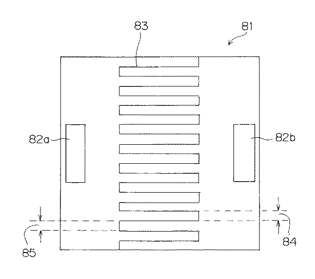
実験1にかかる導電シートモデル81である実施例1を以下のように作成した。
遮水層の厚み、遮水層を構成する樹脂を変更したこと以外は、実施例1と同様の方法で導電シートモデルを作成した。また比較例1は遮水層を形成していない。
実施例1、2、3及び比較例1、2は、以下の評価基準に基づいて評価した。導電シートの両電極を電源と接続し、20Vの電圧を両電極にかけて導電シートが短絡するまでの時間を測定した。なお、測定は室温60℃、湿度95%RHの下で行った。その結果を表1に示す。
実験2にかかる導電シートモデル98である実施例4を以下のように作成した。
遮水層の厚み、遮水層を構成する樹脂を変更したこと以外は、実施例4と同様の方法で導電シートモデルを作成した。
実施例4、5及び比較例3、4、5は、以下の評価基準に基づいて評価した。
R/R0=実験後抵抗値(R)/初期抵抗値(R0)
上記R/R0の値に基づき、電極に発生したクラックを以下の分類に従い評価した。結果を表2に示す。
○: 1≦ R/R0 < 1.1
△: 1.1≦ R/R0 < 1.2
×: 1.2≦ R/R0
10 導電シート
10a 第一検出導電シート
10b 第二検出導電シート
11 透明導電パターン
12 第一ナノファイバー層
16 可視導電パターン
17 第二ナノファイバー層
18 ペースト層
21 遮水層
26 基板
27 第二加熱絶縁層
28 空隙絶縁層
29 第一加熱絶縁層
31、31a、31b シート端子部
32a、32b、32c 個別シート端子
33、33a、33b 引き回し導線部
41a、41b フレキシブルプリント配線板
42 配線板端子部
51 レーザー照射器
61 保護フィルム
62 切り欠き部
63 表示板
81 導電シートモデル
82a、82b 電極形成領域
83 加熱絶縁線
86、87 遮水層
88、89、90 電極形成領域
98 導電シートモデル
110 従来の導電シート
116 従来の可視導電パターン
Claims (6)
- 基板上に透明導電パターンと可視導電パターンを形成した導電シートであって、前記透明導電パターンは金属ナノファイバーを含む層である第一ナノファイバー層と第一ナノファイバー層に隣接した第一加熱絶縁層からなり、前記可視導電パターンは金属ナノファイバーを含む第二ナノファイバー層と第二ナノファイバー層に隣接した第二加熱絶縁層により下層パターンを形成し、前記下層パターンに積層して金属ペーストを含むペースト層からなる上層パターンを形成して構成されていて、第二加熱絶縁層は極小サイズに切断された金属ナノファイバーを含む層である導電シートにおいて、
前記可視導電パターンは、前記下層パターンの上に、前記下層パターンを覆う遮水層を形成し、前記遮水層の上に前記上層パターンを形成した導電シート。 - 請求項1に記載した導電シートにおいて、
前記金属ナノファイバーが銀ナノファイバーであり、
前記金属ペーストが銀ペーストであることを特徴とする請求項1に記載した導電シート。 - 請求項1又は2いずれかに記載した導電シートにおいて、
導電シートにおける引き回し導線部が前記可視導電パターンから構成されている導電シート。 - 導電シートとフレキシブルプリント配線板からなる配線付導電シートにおいて、
請求項1又は2いずれかに記載した導電シートであって、前記導電シートにおけるシート端子部が前記可視導電パターンから構成されていて、前記シート端子部にフレキシブルプリント配線板の接続端子部を電気的に接続した配線付導電シート。 - 請求項4に記載した配線付導電シートをタッチパネル入力装置の電極に使用するタッチパネル入力装置。
- 請求項1にかかる導電シートの製造方法において、
前記可視導電パターンは、以下の工程により製造される導電シートの製造方法。
イ 基板上に金属ナノファイバーを含む層である第二ナノファイバー層を形成する工程
ロ イの工程で形成した第二ナノファイバー層の上に遮水層を形成する工程
ハ ロの工程で形成した遮水層の上に金属ペーストを含む層であるペースト層を形成する工程
ニ ハの工程で形成された第二ナノファイバー層、遮水層とペースト層が形成された基板に、前記ペースト層の上方からエネルギー線を照射して、第二ナノファイバー層中の金属ナノファイバーを切断し、ペースト層中の金属ペーストを焼き切って、前記下層パターンと前記上層パターンを形成する工程。
Priority Applications (6)
| Application Number | Priority Date | Filing Date | Title |
|---|---|---|---|
| JP2011238121A JP5646433B2 (ja) | 2011-10-31 | 2011-10-31 | 導電シート及びその製造方法 |
| KR1020147005806A KR101657951B1 (ko) | 2011-10-31 | 2012-09-27 | 도전시트 및 그 제조방법 |
| US14/354,339 US9591751B2 (en) | 2011-10-31 | 2012-09-27 | Conductive sheet and method for fabricating the same |
| PCT/JP2012/074956 WO2013065430A1 (ja) | 2011-10-31 | 2012-09-27 | 導電シート及びその製造方法 |
| CN201280053595.6A CN104025227B (zh) | 2011-10-31 | 2012-09-27 | 导电片、触摸面板输入装置以及导电片的制造方法 |
| TW101140156A TWI525490B (zh) | 2011-10-31 | 2012-10-30 | Conductive sheet and manufacturing method thereof |
Applications Claiming Priority (1)
| Application Number | Priority Date | Filing Date | Title |
|---|---|---|---|
| JP2011238121A JP5646433B2 (ja) | 2011-10-31 | 2011-10-31 | 導電シート及びその製造方法 |
Publications (2)
| Publication Number | Publication Date |
|---|---|
| JP2013097932A JP2013097932A (ja) | 2013-05-20 |
| JP5646433B2 true JP5646433B2 (ja) | 2014-12-24 |
Family
ID=48191788
Family Applications (1)
| Application Number | Title | Priority Date | Filing Date |
|---|---|---|---|
| JP2011238121A Expired - Fee Related JP5646433B2 (ja) | 2011-10-31 | 2011-10-31 | 導電シート及びその製造方法 |
Country Status (6)
| Country | Link |
|---|---|
| US (1) | US9591751B2 (ja) |
| JP (1) | JP5646433B2 (ja) |
| KR (1) | KR101657951B1 (ja) |
| CN (1) | CN104025227B (ja) |
| TW (1) | TWI525490B (ja) |
| WO (1) | WO2013065430A1 (ja) |
Families Citing this family (25)
| Publication number | Priority date | Publication date | Assignee | Title |
|---|---|---|---|---|
| JP6119518B2 (ja) | 2013-02-12 | 2017-04-26 | ソニー株式会社 | センサ装置、入力装置及び電子機器 |
| US20140262443A1 (en) * | 2013-03-14 | 2014-09-18 | Cambrios Technologies Corporation | Hybrid patterned nanostructure transparent conductors |
| CN105190492B (zh) | 2013-03-18 | 2019-09-27 | 索尼公司 | 传感器装置、输入装置和电子设备 |
| JP6142745B2 (ja) * | 2013-09-10 | 2017-06-07 | ソニー株式会社 | センサ装置、入力装置及び電子機器 |
| CN104516567B (zh) * | 2013-09-29 | 2018-11-02 | 宝宸(厦门)光学科技有限公司 | 触控面板及其制造方法 |
| CN103730296B (zh) * | 2013-11-28 | 2015-11-18 | 江苏省如高高压电器有限公司 | 一种断路器镀银触指电镀挂具 |
| WO2015102415A1 (ko) * | 2013-12-31 | 2015-07-09 | 주식회사 아모그린텍 | 복합 시트 및 그를 구비한 휴대용 단말 |
| US20150209897A1 (en) * | 2014-01-27 | 2015-07-30 | Carestream Health, Inc. | Polarized laser for patterning of silver nanowire transparent conductive films |
| CN106104444B (zh) * | 2014-03-25 | 2019-03-08 | 凸版印刷株式会社 | 透明导电性层叠体及具备透明导电性层叠体的触摸面板 |
| JP2015190859A (ja) | 2014-03-28 | 2015-11-02 | ソニー株式会社 | センサ装置、入力装置及び電子機器 |
| CN104951156A (zh) * | 2014-03-31 | 2015-09-30 | 宸盛光电有限公司 | 电容式触控装置 |
| KR102248460B1 (ko) * | 2014-08-08 | 2021-05-07 | 삼성디스플레이 주식회사 | 터치 스크린 패널 및 그 제조 방법 |
| KR102337828B1 (ko) * | 2014-11-06 | 2021-12-09 | 엘지디스플레이 주식회사 | 터치 패널 및 그를 가지는 터치형 표시 장치 |
| WO2016089159A1 (ko) * | 2014-12-05 | 2016-06-09 | 동우화인켐 주식회사 | 유연 기판 및 이의 제조 방법 |
| KR20160068672A (ko) * | 2014-12-05 | 2016-06-15 | 동우 화인켐 주식회사 | 유연 기판 및 이의 제조 방법 |
| CN104536613B (zh) * | 2015-01-08 | 2017-11-24 | 厦门大学 | 聚偏氟乙烯压电纳米纤维触摸屏敏感元件的制备方法 |
| KR20160100143A (ko) * | 2015-02-13 | 2016-08-23 | 동우 화인켐 주식회사 | 필름 터치 센서 |
| CN106155370B (zh) * | 2015-03-23 | 2019-06-21 | 群创光电股份有限公司 | 触控装置 |
| WO2017179310A1 (ja) * | 2016-04-13 | 2017-10-19 | アルプス電気株式会社 | センサーユニットとそのセンサーユニットを備えた入力装置 |
| US20180338544A1 (en) * | 2017-05-26 | 2018-11-29 | Taiwan Textile Research Institute | Fabric module and smart fabric using the same |
| CN111831156A (zh) * | 2018-01-24 | 2020-10-27 | 祥达光学(厦门)有限公司 | 触控面板与触控传感器卷带 |
| KR102152101B1 (ko) * | 2018-11-02 | 2020-09-07 | 진영글로벌 주식회사 | 차량 전장용 디바이스 |
| KR20210130287A (ko) * | 2020-04-21 | 2021-11-01 | 삼성디스플레이 주식회사 | 윈도우 및 윈도우를 포함하는 표시장치 |
| JP7222437B2 (ja) * | 2020-05-21 | 2023-02-15 | 株式会社村田製作所 | 伸縮性配線基板 |
| KR102870030B1 (ko) * | 2022-02-03 | 2025-11-13 | 주식회사 아모그린텍 | 플렉서블 터치 센서 |
Family Cites Families (10)
| Publication number | Priority date | Publication date | Assignee | Title |
|---|---|---|---|---|
| JPS5724456Y2 (ja) * | 1977-09-09 | 1982-05-27 | ||
| KR100938684B1 (ko) * | 2007-10-16 | 2010-01-25 | 코오롱글로텍주식회사 | 전자 원단 및 이의 제조방법 |
| JP2009099498A (ja) * | 2007-10-19 | 2009-05-07 | Fujitsu Component Ltd | タッチパネル及びタッチパネルの製造方法 |
| JP5259368B2 (ja) * | 2008-12-15 | 2013-08-07 | 日本写真印刷株式会社 | 導電性ナノファイバーシート及びその製造方法 |
| JP5561714B2 (ja) * | 2009-10-13 | 2014-07-30 | 日本写真印刷株式会社 | ディスプレイ電極用透明導電膜 |
| JP5567313B2 (ja) * | 2009-10-29 | 2014-08-06 | 日本写真印刷株式会社 | 立体形状導電性成形品及びその製造方法 |
| JP4780254B2 (ja) * | 2009-12-10 | 2011-09-28 | 凸版印刷株式会社 | 導電性基板およびその製造方法ならびにタッチパネル |
| US9631291B2 (en) * | 2013-01-29 | 2017-04-25 | Hewlett-Packard Development Company, L.P. | Controlling dimensions of nanowires |
| KR102026165B1 (ko) * | 2013-04-26 | 2019-09-27 | 쇼와 덴코 가부시키가이샤 | 도전 패턴의 제조방법 및 도전 패턴 형성 기판 |
| JP2015018624A (ja) * | 2013-07-09 | 2015-01-29 | 日東電工株式会社 | 透明導電性フィルムおよび透明導電性フィルムの製造方法 |
-
2011
- 2011-10-31 JP JP2011238121A patent/JP5646433B2/ja not_active Expired - Fee Related
-
2012
- 2012-09-27 US US14/354,339 patent/US9591751B2/en not_active Expired - Fee Related
- 2012-09-27 KR KR1020147005806A patent/KR101657951B1/ko not_active Expired - Fee Related
- 2012-09-27 CN CN201280053595.6A patent/CN104025227B/zh not_active Expired - Fee Related
- 2012-09-27 WO PCT/JP2012/074956 patent/WO2013065430A1/ja not_active Ceased
- 2012-10-30 TW TW101140156A patent/TWI525490B/zh not_active IP Right Cessation
Also Published As
| Publication number | Publication date |
|---|---|
| KR101657951B1 (ko) | 2016-09-20 |
| TWI525490B (zh) | 2016-03-11 |
| WO2013065430A1 (ja) | 2013-05-10 |
| KR20140106494A (ko) | 2014-09-03 |
| TW201329816A (zh) | 2013-07-16 |
| CN104025227B (zh) | 2016-06-15 |
| US20140299360A1 (en) | 2014-10-09 |
| JP2013097932A (ja) | 2013-05-20 |
| US9591751B2 (en) | 2017-03-07 |
| CN104025227A (zh) | 2014-09-03 |
Similar Documents
| Publication | Publication Date | Title |
|---|---|---|
| JP5646433B2 (ja) | 導電シート及びその製造方法 | |
| TWI444862B (zh) | Face and touch switch | |
| US9448678B2 (en) | Capacitive transparent touch sheet having excellent visibility and durability | |
| JP5361579B2 (ja) | 大型ディスプレイ用のセンサパネル及びその製造方法 | |
| CN102227703B (zh) | 电容触摸屏及用于制作触摸屏的策略性几何形状隔离图案化方法 | |
| JP5590627B2 (ja) | 入力装置 | |
| EP2824546A1 (en) | Flexible touch panel | |
| JP5686405B2 (ja) | 入力装置 | |
| JP2015018317A (ja) | タッチセンサ及びタッチセンサの製造方法 | |
| JP2015064756A (ja) | タッチパネルの製造方法 | |
| KR20150030595A (ko) | 입력 장치 | |
| WO2014046160A1 (ja) | タッチパネル、及びタッチパネルの製造方法 | |
| CN109690457A (zh) | 触摸面板用构件 | |
| JP5542752B2 (ja) | 絶縁部形成方法及び導電パターン形成基板の製造方法 | |
| JP2014013820A (ja) | 導電パターン形成基板 | |
| JP2014026584A (ja) | 透明配線シートおよびその製造方法ならびにタッチパネル用入力部材 | |
| JP2010218137A (ja) | タッチパネル及びその製造方法 | |
| JP6676450B2 (ja) | タッチセンサ及びタッチセンサの製造方法 | |
| US20140118637A1 (en) | Touch panel | |
| JP5800304B2 (ja) | 入力装置 | |
| JP2012227097A (ja) | 静電センサシートの製造方法及び静電センサシート | |
| JP2013247063A (ja) | 導電パターン形成基板およびその製造方法 | |
| JP2013008131A (ja) | 絶縁部形成方法及び導電パターン形成基板の製造方法 | |
| JP5538263B2 (ja) | 導電パターン形成基板およびその製造方法 | |
| KR20140083460A (ko) | 터치패널센서를 위한 적층 구조체의 제조방법 및 적층 구조체 |
Legal Events
| Date | Code | Title | Description |
|---|---|---|---|
| A621 | Written request for application examination |
Free format text: JAPANESE INTERMEDIATE CODE: A621 Effective date: 20140131 |
|
| TRDD | Decision of grant or rejection written | ||
| A01 | Written decision to grant a patent or to grant a registration (utility model) |
Free format text: JAPANESE INTERMEDIATE CODE: A01 Effective date: 20141029 |
|
| A61 | First payment of annual fees (during grant procedure) |
Free format text: JAPANESE INTERMEDIATE CODE: A61 Effective date: 20141105 |
|
| R150 | Certificate of patent or registration of utility model |
Ref document number: 5646433 Country of ref document: JP Free format text: JAPANESE INTERMEDIATE CODE: R150 |
|
| R250 | Receipt of annual fees |
Free format text: JAPANESE INTERMEDIATE CODE: R250 |
|
| S533 | Written request for registration of change of name |
Free format text: JAPANESE INTERMEDIATE CODE: R313533 |
|
| R350 | Written notification of registration of transfer |
Free format text: JAPANESE INTERMEDIATE CODE: R350 |
|
| R250 | Receipt of annual fees |
Free format text: JAPANESE INTERMEDIATE CODE: R250 |
|
| R250 | Receipt of annual fees |
Free format text: JAPANESE INTERMEDIATE CODE: R250 |
|
| R250 | Receipt of annual fees |
Free format text: JAPANESE INTERMEDIATE CODE: R250 |
|
| R250 | Receipt of annual fees |
Free format text: JAPANESE INTERMEDIATE CODE: R250 |
|
| R250 | Receipt of annual fees |
Free format text: JAPANESE INTERMEDIATE CODE: R250 |
|
| LAPS | Cancellation because of no payment of annual fees |