JP5656608B2 - 半導体装置 - Google Patents
半導体装置 Download PDFInfo
- Publication number
- JP5656608B2 JP5656608B2 JP2010281547A JP2010281547A JP5656608B2 JP 5656608 B2 JP5656608 B2 JP 5656608B2 JP 2010281547 A JP2010281547 A JP 2010281547A JP 2010281547 A JP2010281547 A JP 2010281547A JP 5656608 B2 JP5656608 B2 JP 5656608B2
- Authority
- JP
- Japan
- Prior art keywords
- trench
- region
- semiconductor device
- base layer
- layer
- Prior art date
- Legal status (The legal status is an assumption and is not a legal conclusion. Google has not performed a legal analysis and makes no representation as to the accuracy of the status listed.)
- Active
Links
Images




Classifications
-
- H—ELECTRICITY
- H10—SEMICONDUCTOR DEVICES; ELECTRIC SOLID-STATE DEVICES NOT OTHERWISE PROVIDED FOR
- H10D—INORGANIC ELECTRIC SEMICONDUCTOR DEVICES
- H10D64/00—Electrodes of devices having potential barriers
- H10D64/20—Electrodes characterised by their shapes, relative sizes or dispositions
- H10D64/27—Electrodes not carrying the current to be rectified, amplified, oscillated or switched, e.g. gates
- H10D64/311—Gate electrodes for field-effect devices
- H10D64/411—Gate electrodes for field-effect devices for FETs
- H10D64/511—Gate electrodes for field-effect devices for FETs for IGFETs
- H10D64/512—Disposition of the gate electrodes, e.g. buried gates
- H10D64/513—Disposition of the gate electrodes, e.g. buried gates within recesses in the substrate, e.g. trench gates, groove gates or buried gates
-
- H—ELECTRICITY
- H10—SEMICONDUCTOR DEVICES; ELECTRIC SOLID-STATE DEVICES NOT OTHERWISE PROVIDED FOR
- H10D—INORGANIC ELECTRIC SEMICONDUCTOR DEVICES
- H10D12/00—Bipolar devices controlled by the field effect, e.g. insulated-gate bipolar transistors [IGBT]
- H10D12/01—Manufacture or treatment
- H10D12/021—Manufacture or treatment of gated diodes, e.g. field-controlled diodes [FCD]
-
- H—ELECTRICITY
- H10—SEMICONDUCTOR DEVICES; ELECTRIC SOLID-STATE DEVICES NOT OTHERWISE PROVIDED FOR
- H10D—INORGANIC ELECTRIC SEMICONDUCTOR DEVICES
- H10D30/00—Field-effect transistors [FET]
- H10D30/60—Insulated-gate field-effect transistors [IGFET]
- H10D30/64—Double-diffused metal-oxide semiconductor [DMOS] FETs
- H10D30/66—Vertical DMOS [VDMOS] FETs
- H10D30/665—Vertical DMOS [VDMOS] FETs having edge termination structures
-
- H—ELECTRICITY
- H10—SEMICONDUCTOR DEVICES; ELECTRIC SOLID-STATE DEVICES NOT OTHERWISE PROVIDED FOR
- H10D—INORGANIC ELECTRIC SEMICONDUCTOR DEVICES
- H10D30/00—Field-effect transistors [FET]
- H10D30/60—Insulated-gate field-effect transistors [IGFET]
- H10D30/64—Double-diffused metal-oxide semiconductor [DMOS] FETs
- H10D30/66—Vertical DMOS [VDMOS] FETs
- H10D30/668—Vertical DMOS [VDMOS] FETs having trench gate electrodes, e.g. UMOS transistors
-
- H—ELECTRICITY
- H10—SEMICONDUCTOR DEVICES; ELECTRIC SOLID-STATE DEVICES NOT OTHERWISE PROVIDED FOR
- H10D—INORGANIC ELECTRIC SEMICONDUCTOR DEVICES
- H10D64/00—Electrodes of devices having potential barriers
- H10D64/20—Electrodes characterised by their shapes, relative sizes or dispositions
- H10D64/27—Electrodes not carrying the current to be rectified, amplified, oscillated or switched, e.g. gates
- H10D64/311—Gate electrodes for field-effect devices
- H10D64/411—Gate electrodes for field-effect devices for FETs
- H10D64/511—Gate electrodes for field-effect devices for FETs for IGFETs
- H10D64/517—Gate electrodes for field-effect devices for FETs for IGFETs characterised by the conducting layers
- H10D64/519—Gate electrodes for field-effect devices for FETs for IGFETs characterised by the conducting layers characterised by their top-view geometrical layouts
Landscapes
- Electrodes Of Semiconductors (AREA)
- Insulated Gate Type Field-Effect Transistor (AREA)
Description
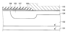
図9は、本発明の前提技術としての、トレンチゲート構造をもつパワーMOSFETのトレンチ終端領域の上面図である。便宜上、ゲート電極107、ソース電極110は一部分を示し、またN+ソース領域は図示を省略している。
図1は、本発明にかかる半導体装置である、トレンチゲート構造をもつパワーMOSFETのトレンチ終端領域の上面図である。便宜上、ゲート電極7とソース電極11は一部分を示し、またN+ソース領域は図示を省略している。
ここで、ゲート絶縁耐量を測定する場合には、ソースとドレインを短絡した状態で、ゲート−ソース間に電圧(Vg)を印加し、電流(Ig)を計測する。また、ドレイン−ソース間の耐圧を測定する場合には、ゲートとソースを短絡した状態で、ドレインに電圧(Vd)を印加し、ドレイン電流(Id)を計測する。このときのドレイン電流をもれ電流とも呼ぶ。
本発明にかかる実施の形態1によれば、半導体装置において、Pベース層4表面からPウェル層3表面へ跨って延在して形成され、Pウェル層3表面に延在方向のトレンチ端部8を有するトレンチ5を備え、トレンチ5は、トレンチ端部8からPベース層4・Pウェル層3境界近傍のPベース層4表面内に跨って延在する第1領域と、Pベース層4表面内において第1領域端部から延在する第2領域とを備え、第1領域は、第2領域よりもそのトレンチ幅が広いことで、トレンチ端部8に尖端形状が形成されることを抑制し、ゲート酸化膜耐量低下や耐圧発振を防止することが可能となる。
Claims (4)
- 第1導電型の半導体基板上に形成された、第1導電型のドリフト層と、
前記ドリフト層表面に選択的に形成された、第2導電型のベース層と、
前記ベース層と隣接して前記ドリフト層表面に形成された、第2導電型のウェル層と、
前記ベース層表面から前記ウェル層表面へ跨って延在して形成され、前記ウェル層表面に延在方向のトレンチ端部を有するトレンチと、
前記トレンチを含む前記ドリフト層上に、選択的に形成されたゲート電極とを備え、
前記トレンチは、前記トレンチ端部から前記ベース層・前記ウェル層境界近傍の前記ベース層表面内に跨って延在する第1領域と、前記ベース層表面内において前記第1領域端部から延在する第2領域とを備え、
前記第1領域は、前記第2領域よりもそのトレンチ幅が広い、
半導体装置。 - 前記第2領域のトレンチ幅は、0.25μm以下である、
請求項1に記載の半導体装置。 - 前記第1領域のトレンチ幅は、0.35μm以上である、
請求項1または2に記載の半導体装置。 - 前記半導体基板は、ワイドバンドギャップ半導体からなる、
請求項1〜3のいずれかに記載の半導体装置。
Priority Applications (5)
| Application Number | Priority Date | Filing Date | Title |
|---|---|---|---|
| JP2010281547A JP5656608B2 (ja) | 2010-12-17 | 2010-12-17 | 半導体装置 |
| US13/205,085 US8530966B2 (en) | 2010-12-17 | 2011-08-08 | Semiconductor device |
| CN201110276618.7A CN102544071B (zh) | 2010-12-17 | 2011-09-05 | 半导体装置 |
| DE102011086733.3A DE102011086733B4 (de) | 2010-12-17 | 2011-11-21 | Halbleitervorrichtung |
| KR1020110130027A KR101319470B1 (ko) | 2010-12-17 | 2011-12-07 | 반도체 장치 |
Applications Claiming Priority (1)
| Application Number | Priority Date | Filing Date | Title |
|---|---|---|---|
| JP2010281547A JP5656608B2 (ja) | 2010-12-17 | 2010-12-17 | 半導体装置 |
Publications (2)
| Publication Number | Publication Date |
|---|---|
| JP2012129446A JP2012129446A (ja) | 2012-07-05 |
| JP5656608B2 true JP5656608B2 (ja) | 2015-01-21 |
Family
ID=46233261
Family Applications (1)
| Application Number | Title | Priority Date | Filing Date |
|---|---|---|---|
| JP2010281547A Active JP5656608B2 (ja) | 2010-12-17 | 2010-12-17 | 半導体装置 |
Country Status (5)
| Country | Link |
|---|---|
| US (1) | US8530966B2 (ja) |
| JP (1) | JP5656608B2 (ja) |
| KR (1) | KR101319470B1 (ja) |
| CN (1) | CN102544071B (ja) |
| DE (1) | DE102011086733B4 (ja) |
Families Citing this family (9)
| Publication number | Priority date | Publication date | Assignee | Title |
|---|---|---|---|---|
| KR101422953B1 (ko) | 2012-12-14 | 2014-08-13 | 삼성전기주식회사 | 전력 반도체 소자 및 그 제조 방법 |
| KR101452091B1 (ko) | 2013-02-26 | 2014-10-16 | 삼성전기주식회사 | 전력 반도체 소자 및 그 제조 방법 |
| JP6020317B2 (ja) * | 2013-04-05 | 2016-11-02 | 三菱電機株式会社 | 半導体素子 |
| JP6360191B2 (ja) * | 2014-10-29 | 2018-07-18 | 株式会社日立製作所 | 電力変換装置 |
| JP6600475B2 (ja) | 2015-03-27 | 2019-10-30 | ローム株式会社 | 半導体装置 |
| JP2018074126A (ja) * | 2016-11-04 | 2018-05-10 | トヨタ自動車株式会社 | 半導体装置 |
| JP6632513B2 (ja) * | 2016-12-07 | 2020-01-22 | 株式会社東芝 | 半導体装置及びその製造方法 |
| JP6967907B2 (ja) | 2017-08-07 | 2021-11-17 | ルネサスエレクトロニクス株式会社 | 半導体装置及び半導体装置の製造方法 |
| JP6876767B2 (ja) * | 2019-10-07 | 2021-05-26 | ローム株式会社 | 半導体装置 |
Family Cites Families (13)
| Publication number | Priority date | Publication date | Assignee | Title |
|---|---|---|---|---|
| JP3904648B2 (ja) | 1997-01-31 | 2007-04-11 | 株式会社ルネサステクノロジ | 半導体装置 |
| US6303410B1 (en) * | 1998-06-01 | 2001-10-16 | North Carolina State University | Methods of forming power semiconductor devices having T-shaped gate electrodes |
| GB0012138D0 (en) * | 2000-05-20 | 2000-07-12 | Koninkl Philips Electronics Nv | A semiconductor device |
| US7576388B1 (en) * | 2002-10-03 | 2009-08-18 | Fairchild Semiconductor Corporation | Trench-gate LDMOS structures |
| JP3931138B2 (ja) * | 2002-12-25 | 2007-06-13 | 三菱電機株式会社 | 電力用半導体装置及び電力用半導体装置の製造方法 |
| US7560359B2 (en) * | 2004-11-26 | 2009-07-14 | Samsung Electronics Co., Ltd. | Methods of forming asymmetric recesses and gate structures that fill such recesses and related methods of forming semiconductor devices that include such recesses and gate structures |
| JP2006229135A (ja) * | 2005-02-21 | 2006-08-31 | Denso Corp | 半導体装置の製造方法 |
| US7276766B2 (en) * | 2005-08-01 | 2007-10-02 | Semiconductor Components Industries, L.L.C. | Semiconductor structure with improved on resistance and breakdown voltage performance |
| JP2007048769A (ja) * | 2005-08-05 | 2007-02-22 | Matsushita Electric Ind Co Ltd | 半導体装置およびその製造方法 |
| JP2005322949A (ja) | 2005-08-05 | 2005-11-17 | Renesas Technology Corp | 半導体装置 |
| US7667265B2 (en) * | 2006-01-30 | 2010-02-23 | Fairchild Semiconductor Corporation | Varying mesa dimensions in high cell density trench MOSFET |
| KR100809332B1 (ko) | 2006-09-04 | 2008-03-05 | 삼성전자주식회사 | 반도체 집적 회로 장치 및 그 제조 방법 |
| JP2009188294A (ja) * | 2008-02-08 | 2009-08-20 | Nec Electronics Corp | パワーmosfet |
-
2010
- 2010-12-17 JP JP2010281547A patent/JP5656608B2/ja active Active
-
2011
- 2011-08-08 US US13/205,085 patent/US8530966B2/en active Active
- 2011-09-05 CN CN201110276618.7A patent/CN102544071B/zh active Active
- 2011-11-21 DE DE102011086733.3A patent/DE102011086733B4/de active Active
- 2011-12-07 KR KR1020110130027A patent/KR101319470B1/ko active Active
Also Published As
| Publication number | Publication date |
|---|---|
| DE102011086733A1 (de) | 2012-06-21 |
| CN102544071B (zh) | 2014-11-05 |
| JP2012129446A (ja) | 2012-07-05 |
| KR101319470B1 (ko) | 2013-10-17 |
| US20120153382A1 (en) | 2012-06-21 |
| KR20120068701A (ko) | 2012-06-27 |
| DE102011086733B4 (de) | 2020-03-26 |
| CN102544071A (zh) | 2012-07-04 |
| US8530966B2 (en) | 2013-09-10 |
Similar Documents
| Publication | Publication Date | Title |
|---|---|---|
| JP5656608B2 (ja) | 半導体装置 | |
| CN105280711B (zh) | 电荷补偿结构及用于其的制造 | |
| US10672878B2 (en) | Silicon carbide semiconductor device | |
| CN107527943B (zh) | 功率半导体装置 | |
| CN103426910B (zh) | 功率半导体元件及其边缘终端结构 | |
| JP7345354B2 (ja) | 半導体装置 | |
| JP2009038318A (ja) | 半導体装置 | |
| JP2012064849A (ja) | 半導体装置 | |
| CN114725219B (zh) | 碳化硅沟槽栅晶体管及其制造方法 | |
| JP6183550B2 (ja) | 半導体装置 | |
| JP2013065749A (ja) | 半導体装置 | |
| KR20120005712U (ko) | 쇼트키 다이오드의 종단 영역 트렌치 구조 | |
| JP2020025050A (ja) | 半導体装置 | |
| JP5957171B2 (ja) | 半導体装置及びその製造方法 | |
| JP7330396B2 (ja) | 半導体装置及び電力変換装置 | |
| CN105097936A (zh) | 一种绝缘层上硅ldmos功率器件 | |
| JP7321820B2 (ja) | 半導体装置、インバータ回路、駆動装置、車両、及び、昇降機 | |
| CN120021379A (zh) | 晶体管构件和用于制造晶体管构件的方法 | |
| KR101616157B1 (ko) | 전력 반도체 소자 및 그 제조 방법 | |
| TW201724503A (zh) | 具有超晶格結構的表面優化電晶體 | |
| US12166082B2 (en) | Silicon carbide semiconductor power transistor and method of manufacturing the same | |
| CN115799309A (zh) | 一种具有背侧超结层的SiC MOSFET结构 | |
| JP2023074678A (ja) | 半導体装置 | |
| CN113410281A (zh) | 一种具有表面耐压结构的p沟道LDMOS器件及其制备方法 | |
| CN113410298B (zh) | 一种具有表面耐压结构的n沟道LDMOS器件及其制备方法 |
Legal Events
| Date | Code | Title | Description |
|---|---|---|---|
| A621 | Written request for application examination |
Free format text: JAPANESE INTERMEDIATE CODE: A621 Effective date: 20130325 |
|
| A977 | Report on retrieval |
Free format text: JAPANESE INTERMEDIATE CODE: A971007 Effective date: 20140313 |
|
| A131 | Notification of reasons for refusal |
Free format text: JAPANESE INTERMEDIATE CODE: A131 Effective date: 20140401 |
|
| TRDD | Decision of grant or rejection written | ||
| A01 | Written decision to grant a patent or to grant a registration (utility model) |
Free format text: JAPANESE INTERMEDIATE CODE: A01 Effective date: 20141028 |
|
| A61 | First payment of annual fees (during grant procedure) |
Free format text: JAPANESE INTERMEDIATE CODE: A61 Effective date: 20141125 |
|
| R150 | Certificate of patent or registration of utility model |
Ref document number: 5656608 Country of ref document: JP Free format text: JAPANESE INTERMEDIATE CODE: R150 |
|
| R250 | Receipt of annual fees |
Free format text: JAPANESE INTERMEDIATE CODE: R250 |
|
| R250 | Receipt of annual fees |
Free format text: JAPANESE INTERMEDIATE CODE: R250 |
|
| R250 | Receipt of annual fees |
Free format text: JAPANESE INTERMEDIATE CODE: R250 |
|
| R250 | Receipt of annual fees |
Free format text: JAPANESE INTERMEDIATE CODE: R250 |
|
| R250 | Receipt of annual fees |
Free format text: JAPANESE INTERMEDIATE CODE: R250 |
|
| R250 | Receipt of annual fees |
Free format text: JAPANESE INTERMEDIATE CODE: R250 |
|
| R250 | Receipt of annual fees |
Free format text: JAPANESE INTERMEDIATE CODE: R250 |
|
| R250 | Receipt of annual fees |
Free format text: JAPANESE INTERMEDIATE CODE: R250 |
|
| R250 | Receipt of annual fees |
Free format text: JAPANESE INTERMEDIATE CODE: R250 |