JP5657352B2 - 露光量評価方法および反射型基板 - Google Patents
露光量評価方法および反射型基板 Download PDFInfo
- Publication number
- JP5657352B2 JP5657352B2 JP2010252134A JP2010252134A JP5657352B2 JP 5657352 B2 JP5657352 B2 JP 5657352B2 JP 2010252134 A JP2010252134 A JP 2010252134A JP 2010252134 A JP2010252134 A JP 2010252134A JP 5657352 B2 JP5657352 B2 JP 5657352B2
- Authority
- JP
- Japan
- Prior art keywords
- light
- euv
- exposure
- substrate
- long
- Prior art date
- Legal status (The legal status is an assumption and is not a legal conclusion. Google has not performed a legal analysis and makes no representation as to the accuracy of the status listed.)
- Expired - Fee Related
Links
Images





Classifications
-
- G—PHYSICS
- G03—PHOTOGRAPHY; CINEMATOGRAPHY; ANALOGOUS TECHNIQUES USING WAVES OTHER THAN OPTICAL WAVES; ELECTROGRAPHY; HOLOGRAPHY
- G03F—PHOTOMECHANICAL PRODUCTION OF TEXTURED OR PATTERNED SURFACES, e.g. FOR PRINTING, FOR PROCESSING OF SEMICONDUCTOR DEVICES; MATERIALS THEREFOR; ORIGINALS THEREFOR; APPARATUS SPECIALLY ADAPTED THEREFOR
- G03F1/00—Originals for photomechanical production of textured or patterned surfaces, e.g., masks, photo-masks, reticles; Mask blanks or pellicles therefor; Containers specially adapted therefor; Preparation thereof
- G03F1/22—Masks or mask blanks for imaging by radiation of 100nm or shorter wavelength, e.g. X-ray masks, extreme ultraviolet [EUV] masks; Preparation thereof
- G03F1/24—Reflection masks; Preparation thereof
-
- G—PHYSICS
- G01—MEASURING; TESTING
- G01J—MEASUREMENT OF INTENSITY, VELOCITY, SPECTRAL CONTENT, POLARISATION, PHASE OR PULSE CHARACTERISTICS OF INFRARED, VISIBLE OR ULTRAVIOLET LIGHT; COLORIMETRY; RADIATION PYROMETRY
- G01J1/00—Photometry, e.g. photographic exposure meter
- G01J1/42—Photometry, e.g. photographic exposure meter using electric radiation detectors
- G01J1/429—Photometry, e.g. photographic exposure meter using electric radiation detectors applied to measurement of ultraviolet light
-
- G—PHYSICS
- G03—PHOTOGRAPHY; CINEMATOGRAPHY; ANALOGOUS TECHNIQUES USING WAVES OTHER THAN OPTICAL WAVES; ELECTROGRAPHY; HOLOGRAPHY
- G03F—PHOTOMECHANICAL PRODUCTION OF TEXTURED OR PATTERNED SURFACES, e.g. FOR PRINTING, FOR PROCESSING OF SEMICONDUCTOR DEVICES; MATERIALS THEREFOR; ORIGINALS THEREFOR; APPARATUS SPECIALLY ADAPTED THEREFOR
- G03F1/00—Originals for photomechanical production of textured or patterned surfaces, e.g., masks, photo-masks, reticles; Mask blanks or pellicles therefor; Containers specially adapted therefor; Preparation thereof
- G03F1/68—Preparation processes not covered by groups G03F1/20 - G03F1/50
- G03F1/82—Auxiliary processes, e.g. cleaning or inspecting
- G03F1/84—Inspecting
-
- G—PHYSICS
- G03—PHOTOGRAPHY; CINEMATOGRAPHY; ANALOGOUS TECHNIQUES USING WAVES OTHER THAN OPTICAL WAVES; ELECTROGRAPHY; HOLOGRAPHY
- G03F—PHOTOMECHANICAL PRODUCTION OF TEXTURED OR PATTERNED SURFACES, e.g. FOR PRINTING, FOR PROCESSING OF SEMICONDUCTOR DEVICES; MATERIALS THEREFOR; ORIGINALS THEREFOR; APPARATUS SPECIALLY ADAPTED THEREFOR
- G03F7/00—Photomechanical, e.g. photolithographic, production of textured or patterned surfaces, e.g. printing surfaces; Materials therefor, e.g. comprising photoresists; Apparatus specially adapted therefor
- G03F7/70—Microphotolithographic exposure; Apparatus therefor
- G03F7/70483—Information management; Active and passive control; Testing; Wafer monitoring, e.g. pattern monitoring
- G03F7/70605—Workpiece metrology
- G03F7/70616—Monitoring the printed patterns
- G03F7/70625—Dimensions, e.g. line width, critical dimension [CD], profile, sidewall angle or edge roughness
-
- G—PHYSICS
- G03—PHOTOGRAPHY; CINEMATOGRAPHY; ANALOGOUS TECHNIQUES USING WAVES OTHER THAN OPTICAL WAVES; ELECTROGRAPHY; HOLOGRAPHY
- G03F—PHOTOMECHANICAL PRODUCTION OF TEXTURED OR PATTERNED SURFACES, e.g. FOR PRINTING, FOR PROCESSING OF SEMICONDUCTOR DEVICES; MATERIALS THEREFOR; ORIGINALS THEREFOR; APPARATUS SPECIALLY ADAPTED THEREFOR
- G03F7/00—Photomechanical, e.g. photolithographic, production of textured or patterned surfaces, e.g. printing surfaces; Materials therefor, e.g. comprising photoresists; Apparatus specially adapted therefor
- G03F7/70—Microphotolithographic exposure; Apparatus therefor
- G03F7/708—Construction of apparatus, e.g. environment aspects, hygiene aspects or materials
- G03F7/7085—Detection arrangement, e.g. detectors of apparatus alignment possibly mounted on wafers, exposure dose, photo-cleaning flux, stray light, thermal load
-
- G—PHYSICS
- G03—PHOTOGRAPHY; CINEMATOGRAPHY; ANALOGOUS TECHNIQUES USING WAVES OTHER THAN OPTICAL WAVES; ELECTROGRAPHY; HOLOGRAPHY
- G03F—PHOTOMECHANICAL PRODUCTION OF TEXTURED OR PATTERNED SURFACES, e.g. FOR PRINTING, FOR PROCESSING OF SEMICONDUCTOR DEVICES; MATERIALS THEREFOR; ORIGINALS THEREFOR; APPARATUS SPECIALLY ADAPTED THEREFOR
- G03F7/00—Photomechanical, e.g. photolithographic, production of textured or patterned surfaces, e.g. printing surfaces; Materials therefor, e.g. comprising photoresists; Apparatus specially adapted therefor
- G03F7/70—Microphotolithographic exposure; Apparatus therefor
- G03F7/708—Construction of apparatus, e.g. environment aspects, hygiene aspects or materials
- G03F7/70908—Hygiene, e.g. preventing apparatus pollution, mitigating effect of pollution or removing pollutants from apparatus
- G03F7/70941—Stray fields and charges, e.g. stray light, scattered light, flare, transmission loss
Landscapes
- General Physics & Mathematics (AREA)
- Physics & Mathematics (AREA)
- Epidemiology (AREA)
- Health & Medical Sciences (AREA)
- Public Health (AREA)
- Engineering & Computer Science (AREA)
- Environmental & Geological Engineering (AREA)
- Life Sciences & Earth Sciences (AREA)
- Atmospheric Sciences (AREA)
- Spectroscopy & Molecular Physics (AREA)
- Preparing Plates And Mask In Photomechanical Process (AREA)
- Exposure And Positioning Against Photoresist Photosensitive Materials (AREA)
- Exposure Of Semiconductors, Excluding Electron Or Ion Beam Exposure (AREA)
- Photometry And Measurement Of Optical Pulse Characteristics (AREA)
Description
図1は、EUV露光装置の構成を示す図である。EUV露光装置1は、ウエハ20などの基板にEUV光を照射して、EUV露光を行う装置である。EUV露光装置1は、製品ウエハ(図示せず)への露光を行う際には、回路パターン(マスクパターン)が形成されたマスク(図示せず)を用いて、製品ウエハへの露光を行う。また、EUV露光装置1は、DUV光などのEUV光以外の長波長を有したOutband(DUV光など)を評価する際には、露光量評価用のマスク(フォトマスク)2Xを用いて、ウエハ20への露光を行う。
P<λ/{(1+σ)NA}・・・(1)
Claims (9)
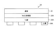
- 露光光のうちEUV光よりも長い波長を有した長波長光を反射し且つ前記EUV光を吸収する長波長光反射膜と、前記長波長光反射膜の上層側に配置されるとともに前記EUV光および前記長波長光を吸収する吸収膜を用いて形成されたマスクパターンとを有したフォトマスクと、レジストが塗布された露光対象の基板と、をEUV露光装置内にセットするセットステップと、
前記フォトマスクに対し前記マスクパターン側から前記露光光を照射するとともに、前記フォトマスクで反射された露光光を前記基板に照射する照射ステップと、
前記基板に照射された露光光の露光量に基づいて、前記基板に照射された長波長光の光量分布を測定する光量測定ステップと、
を含むことを特徴とする露光量評価方法。 - 露光光のうちEUV光よりも長い波長を有した長波長光および前記EUV光を吸収する吸収膜と、前記吸収膜の上層側に配置されるとともに前記EUV光を吸収し且つ前記長波長光を反射する長波長光反射膜を用いて形成されたマスクパターンとを有したフォトマスクと、レジストが塗布された露光対象の基板と、をEUV露光装置内にセットするセットステップと、
前記フォトマスクに対し前記マスクパターン側から前記露光光を照射するとともに、前記フォトマスクで反射された露光光を前記基板に照射する照射ステップと、
前記基板に照射された露光光の露光量に基づいて、前記基板に照射された長波長光の光量分布を測定する光量測定ステップと、
を含むことを特徴とする露光量評価方法。 - 前記フォトマスクで反射された露光光が照射された基板を現像することによって、前記基板上に前記マスクパターンに応じた転写パターンを形成する転写パターン形成ステップをさらに含み、
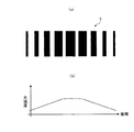
前記光量測定ステップは、前記転写パターンのパターン形状に基づいて、前記基板に照射された長波長光の光量分布を測定することを特徴とする請求項1または2に記載の露光量評価方法。 - 前記マスクパターンは、所定の周期でラインパターンとスペース領域とが交互に配置されたパターン形状を有していることを特徴とする請求項1〜3のいずれか1つに記載の露光量評価方法。
- 前記周期は、前記長波長光の波長領域の中心波長をλとし、前記EUV露光装置の投影光学系開口数をNAとし、前記露光光の有効光源の大きさをσとし、前記周期をPとした場合に、P<λ/{(1+σ)NA}の関係を有していることを特徴とする請求項4に記載の露光量評価方法。
- 前記吸収膜は、Cr、C、Cr/CrO、SiO、SiNまたはCr/Fを含んで構成されていることを特徴とする請求項1に記載の露光量評価方法。
- 前記長波長光反射膜は、Taを含んで構成されていることを特徴とする請求項2に記載の露光量評価方法。
- EUV露光装置の反射マスク位置に装着可能な反射型基板であって、
露光光のうちEUV光よりも長い波長を有した長波長光の露光量の評価に用いられるとともに、
前記EUV光に対して反射性を有するマスク基板の上層に、
前記長波長光を反射し且つ前記EUV光を吸収する長波長光反射膜と、
前記長波長光反射膜の上層側に配置されるとともに前記EUV光および前記長波長光を吸収する吸収膜を用いて形成されたマスクパターンと、
が形成されていることを特徴とする反射型基板。 - EUV露光装置の反射マスク位置に装着可能な反射型基板であって、
露光光のうちEUV光よりも長い波長を有した長波長光の露光量の評価に用いられるとともに、
前記長波長光および前記EUV光を吸収する基板の上層に、
前記EUV光に対して反射性を有する膜で形成されたマスクパターンと、
前記反射膜で形成されたマスクパターンの上層側に配置されるとともに前記EUV光を吸収し且つ前記長波長光を反射する長波長光反射膜と、
が形成されていることを特徴とする反射型基板。
Priority Applications (3)
| Application Number | Priority Date | Filing Date | Title |
|---|---|---|---|
| JP2010252134A JP5657352B2 (ja) | 2010-11-10 | 2010-11-10 | 露光量評価方法および反射型基板 |
| US13/237,736 US9110374B2 (en) | 2010-11-10 | 2011-09-20 | Exposure amount evaluation method and photomask |
| US14/795,923 US9250512B2 (en) | 2010-11-10 | 2015-07-10 | Exposure amount evaluation method and photomask |
Applications Claiming Priority (1)
| Application Number | Priority Date | Filing Date | Title |
|---|---|---|---|
| JP2010252134A JP5657352B2 (ja) | 2010-11-10 | 2010-11-10 | 露光量評価方法および反射型基板 |
Publications (2)
| Publication Number | Publication Date |
|---|---|
| JP2012104670A JP2012104670A (ja) | 2012-05-31 |
| JP5657352B2 true JP5657352B2 (ja) | 2015-01-21 |
Family
ID=46018715
Family Applications (1)
| Application Number | Title | Priority Date | Filing Date |
|---|---|---|---|
| JP2010252134A Expired - Fee Related JP5657352B2 (ja) | 2010-11-10 | 2010-11-10 | 露光量評価方法および反射型基板 |
Country Status (2)
| Country | Link |
|---|---|
| US (2) | US9110374B2 (ja) |
| JP (1) | JP5657352B2 (ja) |
Families Citing this family (3)
| Publication number | Priority date | Publication date | Assignee | Title |
|---|---|---|---|---|
| DE102014216121A1 (de) * | 2014-08-13 | 2016-02-18 | Carl Zeiss Smt Gmbh | Maske für die EUV-Lithographie, EUV-Lithographieanlage und Verfahren zum Bestimmen eines durch DUV-Strahlung hervorgerufenen Kontrastanteils |
| WO2018091189A2 (en) * | 2016-11-15 | 2018-05-24 | Asml Netherlands B.V. | Radiation analysis system |
| JP7506114B2 (ja) | 2022-07-01 | 2024-06-25 | アルバック成膜株式会社 | マスクブランクスの製造方法及びマスクブランクス、フォトマスク |
Family Cites Families (18)
| Publication number | Priority date | Publication date | Assignee | Title |
|---|---|---|---|---|
| JPH04151818A (ja) * | 1990-10-16 | 1992-05-25 | Canon Inc | リソグラフィー用マスク構造体の製造方法 |
| JP3250415B2 (ja) * | 1995-04-28 | 2002-01-28 | 凸版印刷株式会社 | ハーフトーン型位相シフトマスクの製造方法 |
| JP3302926B2 (ja) | 1998-07-02 | 2002-07-15 | 株式会社東芝 | 露光装置の検査方法 |
| JP3674591B2 (ja) | 2002-02-25 | 2005-07-20 | ソニー株式会社 | 露光用マスクの製造方法および露光用マスク |
| EP1426824A1 (en) * | 2002-12-04 | 2004-06-09 | ASML Netherlands B.V. | Lithographic apparatus, device manufacturing method, and device manufactured thereby |
| WO2005008754A1 (ja) * | 2003-07-18 | 2005-01-27 | Nikon Corporation | フレア計測方法、露光方法、及びフレア計測用のマスク |
| US7034923B2 (en) | 2004-01-21 | 2006-04-25 | Asml Netherlands B.V. | Optical element, lithographic apparatus comprising such optical element and device manufacturing method |
| JP4635610B2 (ja) * | 2005-01-07 | 2011-02-23 | 凸版印刷株式会社 | 反射型フォトマスクブランク、反射型フォトマスク、及び反射型フォトマスクの製造方法 |
| JP2006237184A (ja) * | 2005-02-24 | 2006-09-07 | Sony Corp | マスク補正方法および露光用マスク |
| JP2007206333A (ja) * | 2006-02-01 | 2007-08-16 | Elpida Memory Inc | フレア測定用マスク及びフレア測定方法 |
| JP2008041740A (ja) | 2006-08-02 | 2008-02-21 | Toppan Printing Co Ltd | 反射型フォトマスクブランク、反射型フォトマスク及び極端紫外線の露光方法 |
| JP2008198788A (ja) * | 2007-02-13 | 2008-08-28 | Toshiba Corp | レジストパターン形成方法 |
| US8018578B2 (en) * | 2007-04-19 | 2011-09-13 | Asml Netherlands B.V. | Pellicle, lithographic apparatus and device manufacturing method |
| JP5018212B2 (ja) * | 2007-04-26 | 2012-09-05 | 凸版印刷株式会社 | 反射型フォトマスクブランク及び反射型フォトマスク並びに半導体装置の製造方法 |
| NL1036695A1 (nl) | 2008-05-15 | 2009-11-17 | Asml Netherlands Bv | Lithographic apparatus. |
| CN102187275B (zh) * | 2008-11-26 | 2013-09-04 | Hoya株式会社 | 掩模板用基板、掩模板用基板组及半导体器件的制造方法 |
| JP5330019B2 (ja) * | 2009-02-18 | 2013-10-30 | ルネサスエレクトロニクス株式会社 | マスクパターンの検査方法およびマスクパターン検査装置 |
| JP5397596B2 (ja) * | 2009-03-03 | 2014-01-22 | 株式会社ニコン | フレア計測方法及び露光方法 |
-
2010
- 2010-11-10 JP JP2010252134A patent/JP5657352B2/ja not_active Expired - Fee Related
-
2011
- 2011-09-20 US US13/237,736 patent/US9110374B2/en active Active
-
2015
- 2015-07-10 US US14/795,923 patent/US9250512B2/en active Active
Also Published As
| Publication number | Publication date |
|---|---|
| US9250512B2 (en) | 2016-02-02 |
| US9110374B2 (en) | 2015-08-18 |
| US20150331308A1 (en) | 2015-11-19 |
| US20120112085A1 (en) | 2012-05-10 |
| JP2012104670A (ja) | 2012-05-31 |
Similar Documents
| Publication | Publication Date | Title |
|---|---|---|
| US11487198B2 (en) | Patterning device, a method of making the same, and a patterning device design method | |
| US7376512B2 (en) | Method for determining an optimal absorber stack geometry of a lithographic reflection mask | |
| US7327436B2 (en) | Method for evaluating a local flare, correction method for a mask pattern, manufacturing method for a semiconductor device and a computer program product | |
| KR100541487B1 (ko) | 광학계의 조정방법 및 장치, 노광장치 | |
| JP5485262B2 (ja) | アライメントフィーチャ、プリ・アライメント方法、及びリソグラフィ装置 | |
| JP7535577B2 (ja) | 構造化物体の表面にわたる測定光波長の測定光の光学的位相差を決定するための方法 | |
| CN113494966A (zh) | 测量euv掩模的相位的装置和方法及制造掩模的方法 | |
| KR101713382B1 (ko) | 극자외선 리소그래피 공정 및 마스크 | |
| JP2009272347A (ja) | 光反射型マスク、露光装置、測定方法、及び半導体装置の製造方法 | |
| US6627356B2 (en) | Photomask used in manufacturing of semiconductor device, photomask blank, and method of applying light exposure to semiconductor wafer by using said photomask | |
| JP4339841B2 (ja) | リソグラフィ装置及びデバイス製造方法 | |
| US9250512B2 (en) | Exposure amount evaluation method and photomask | |
| JP6609307B2 (ja) | Euvリソグラフィ用マスク、euvリソグラフィ装置、及びduv放射線に起因するコントラスト比を求める方法 | |
| KR20150113809A (ko) | 노출 강도를 조정함으로써 극성 불균형을 감소시키는 방법 및 시스템 | |
| TW202422214A (zh) | 抑制遮罩吸收劑之鏡面反射及解析度上場拼接 | |
| CN113557477B (zh) | 光刻设备、量测设备、光学系统和方法 | |
| KR20250118680A (ko) | 오버레이 보정 방법 및 그 보정 방법을 포함한 노광 방법 | |
| US10802395B2 (en) | Lithographic mask, a pellicle therein and method of forming the same | |
| Lee et al. | Multistack structure for an extreme-ultraviolet pellicle with out-of-band radiation reduction | |
| Tirapu-Azpiroz et al. | Understanding the trade-offs of thinner binary mask absorbers | |
| JP2010205886A (ja) | 露光装置のフレア評価方法 | |
| JP2004134444A (ja) | 極短紫外線光学系の光学特性測定方法及び装置、並びに極短紫外線光学系の製造方法 | |
| KR20100076688A (ko) | 극자외선 리소그래피를 위한 마스크의 패턴 임계치수 보정방법 | |
| KR20100073093A (ko) | 플레어 계측 레티클, 플레어 센싱 모듈 및 극자외선 리소그래피를 위한 노광 장치 | |
| KR20090068009A (ko) | 반사형 포토마스크의 선폭 균일도 보정방법 |
Legal Events
| Date | Code | Title | Description |
|---|---|---|---|
| A621 | Written request for application examination |
Free format text: JAPANESE INTERMEDIATE CODE: A621 Effective date: 20130220 |
|
| A977 | Report on retrieval |
Free format text: JAPANESE INTERMEDIATE CODE: A971007 Effective date: 20131113 |
|
| A131 | Notification of reasons for refusal |
Free format text: JAPANESE INTERMEDIATE CODE: A131 Effective date: 20131126 |
|
| A521 | Request for written amendment filed |
Free format text: JAPANESE INTERMEDIATE CODE: A523 Effective date: 20131226 |
|
| A131 | Notification of reasons for refusal |
Free format text: JAPANESE INTERMEDIATE CODE: A131 Effective date: 20140729 |
|
| A521 | Request for written amendment filed |
Free format text: JAPANESE INTERMEDIATE CODE: A523 Effective date: 20140924 |
|
| TRDD | Decision of grant or rejection written | ||
| A01 | Written decision to grant a patent or to grant a registration (utility model) |
Free format text: JAPANESE INTERMEDIATE CODE: A01 Effective date: 20141028 |
|
| A61 | First payment of annual fees (during grant procedure) |
Free format text: JAPANESE INTERMEDIATE CODE: A61 Effective date: 20141126 |
|
| R151 | Written notification of patent or utility model registration |
Ref document number: 5657352 Country of ref document: JP Free format text: JAPANESE INTERMEDIATE CODE: R151 |
|
| S111 | Request for change of ownership or part of ownership |
Free format text: JAPANESE INTERMEDIATE CODE: R313111 |
|
| R350 | Written notification of registration of transfer |
Free format text: JAPANESE INTERMEDIATE CODE: R350 |
|
| S111 | Request for change of ownership or part of ownership |
Free format text: JAPANESE INTERMEDIATE CODE: R313111 |
|
| R350 | Written notification of registration of transfer |
Free format text: JAPANESE INTERMEDIATE CODE: R350 |
|
| LAPS | Cancellation because of no payment of annual fees |