JP5666192B2 - 電流センサ - Google Patents
電流センサ Download PDFInfo
- Publication number
- JP5666192B2 JP5666192B2 JP2010174878A JP2010174878A JP5666192B2 JP 5666192 B2 JP5666192 B2 JP 5666192B2 JP 2010174878 A JP2010174878 A JP 2010174878A JP 2010174878 A JP2010174878 A JP 2010174878A JP 5666192 B2 JP5666192 B2 JP 5666192B2
- Authority
- JP
- Japan
- Prior art keywords
- core
- core piece
- current sensor
- gap
- piece
- Prior art date
- Legal status (The legal status is an assumption and is not a legal conclusion. Google has not performed a legal analysis and makes no representation as to the accuracy of the status listed.)
- Expired - Fee Related
Links
- 230000004907 flux Effects 0.000 claims description 55
- 238000001514 detection method Methods 0.000 claims description 34
- 239000000463 material Substances 0.000 description 6
- 238000010586 diagram Methods 0.000 description 5
- 230000009467 reduction Effects 0.000 description 5
- XEEYBQQBJWHFJM-UHFFFAOYSA-N Iron Chemical compound [Fe] XEEYBQQBJWHFJM-UHFFFAOYSA-N 0.000 description 4
- 230000000694 effects Effects 0.000 description 4
- 238000003780 insertion Methods 0.000 description 4
- 230000037431 insertion Effects 0.000 description 4
- 238000004088 simulation Methods 0.000 description 4
- 229910000831 Steel Inorganic materials 0.000 description 3
- 239000010959 steel Substances 0.000 description 3
- 229910052742 iron Inorganic materials 0.000 description 2
- 230000002093 peripheral effect Effects 0.000 description 2
- 230000035699 permeability Effects 0.000 description 2
- 239000011347 resin Substances 0.000 description 2
- 229920005989 resin Polymers 0.000 description 2
- 239000003566 sealing material Substances 0.000 description 2
- 230000005355 Hall effect Effects 0.000 description 1
- 229910045601 alloy Inorganic materials 0.000 description 1
- 239000000956 alloy Substances 0.000 description 1
- 238000004141 dimensional analysis Methods 0.000 description 1
- 238000007599 discharging Methods 0.000 description 1
- 238000007429 general method Methods 0.000 description 1
- 238000010030 laminating Methods 0.000 description 1
- 239000000696 magnetic material Substances 0.000 description 1
- 238000012986 modification Methods 0.000 description 1
- 230000004048 modification Effects 0.000 description 1
- 238000000465 moulding Methods 0.000 description 1
- 229910000889 permalloy Inorganic materials 0.000 description 1
- 238000005549 size reduction Methods 0.000 description 1
- 239000013585 weight reducing agent Substances 0.000 description 1
- 229910000859 α-Fe Inorganic materials 0.000 description 1
Images




Landscapes
- Measuring Instrument Details And Bridges, And Automatic Balancing Devices (AREA)
Description
また、磁気センサがコア片に固定されているため、コア片を位置決めすると磁気センサも位置決めされる。このため、従来のように磁気センサ自体で位置決めする場合に比べ、磁気センサの位置決め精度が向上する。これにより、電流センサの検出精度が向上する。なお、コア片の位置決めは、コアと一体で樹脂モールドなどの一般的な方法で行えばよい。
まず、第1の実施の形態について説明する。そこで、第1の実施の形態に係る電流センサについて、図1を参照しながら説明する。図1は、第1の実施の形態に係る電流センサの全体構成を示す図である。
図1に示すように、本実施の形態に係る電流センサ1は、コア10、コア片11、ホール素子12a,12b、筺体14、電子部品16、配線材18などを有している。
なお、コア10とコア片11とをそれぞれ異なる材質(透磁率が異なる)で形成することもできる。このような場合でも、磁束密度への影響はほとんどない。但し、材料の飽和磁束密度については性能に影響があるため、大電流を検知する場合には、コア10及びコア片11の材質として、高飽和磁束密度の材料を用いることが好ましい。
まず、導電部材(例えば、バスバー)などの検出対象物22を収容部24の挿通孔28内に貫通させるようにして挿入する。
次に、電流センサ1の検出信号を入力する外部装置(不図示)のコネクタ(不図示)をコネクタ装着部26に挿入し、外部装置とコネクタ装着部26内のコネクタ端子27とを接続する。
このようにして電流センサ1は、環状のコア10に挿通された検出対象物22に流れる電流の電流値を、コア10のギャップ20内に設けられたホール素子12a,12bによって検出する。そして、各ホール素子12a,12bを通過する磁束密度が均一であるため、検出対象物22に流れる電流の電流値を精度良く検出することができる。
次に、第2の実施の形態について説明する。第2の実施の形態は、第1の実施の形態と基本的な構成はほぼ同じであるが、ホール素子を1つとした点が異なっている。そのため、以下では、第1の実施の形態と同じ構成については図面に同じ符号を付してその説明を適宜省略し、第1の実施の形態との相違点について説明する。そこで、第2の実施の形態に係る電流センサについて、図8を参照しながら説明する。図8は、第2の実施の形態に係る電流センサの主要部を示す図である。
最後に、第3の実施の形態について説明する。第3の実施の形態は、第2の実施の形態と基本的な構成はほぼ同じであるが、ホール素子をコア片に密着させていない点が異なっている。そのため、以下では、第2の実施の形態と同じ構成については図面に同じ符号を付してその説明を適宜省略し、第2の実施の形態との相違点について説明する。そこで、第3の実施の形態に係る電流センサについて、図9を参照しながら説明する。図9は、第3の実施の形態に係る電流センサの主要部を示す図である。
また、第3の実施の形態でも第2の実施の形態と同様に、第1の実施の形態に比べて検出精度は若干低下するが、更なる低コスト化を図ることができる。
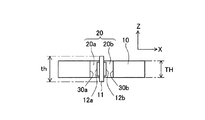
10 コア
11 コア片
12,12a,12b ホール素子
20,20a,20b ギャップ
30a,30b コア端面
TH コアの厚さ(コア端面のZ方向の大きさ)
th コア片の厚さ(Z方向の大きさ)
W コアの幅(コア端面のY方向の大きさ)
w コア片の幅(Y方向の大きさ)
Claims (6)
- ギャップを備え環状に形成され、その環状内側に挿入される検出対象物に流れる電流により発生する磁束の磁路となるコアと、前記ギャップ内に設けられ、前記ギャップ内の磁界の強さに応じた電気信号を発生する磁気センサとを有する電流センサにおいて、
前記ギャップにて対向するコア端面間に、前記各コア端面に対向するように配置される1つのコア片を備え、
前記コア片の厚さ及び幅が、前記コア端面の厚さ及び幅より小さくなく、かつ前記コア端面に対向する前記コア片の断面積が、前記コア端面の断面積よりも大きく、
前記コア片は、前記コアの両端面から前記コア片の両側にギャップを介して配置され、少なくとも一方のギャップに前記磁気センサが配置されており、
前記磁気センサの断面積は、前記コア端面の断面積よりも小さい
ことを特徴とする電流センサ。 - 請求項1に記載する電流センサにおいて、
前記コア片の厚さと前記コア端面の厚さとの比、あるいは前記コア片の幅と前記コア端面の幅との比の少なくとも一方が、1.15以上である
ことを特徴とする電流センサ。 - 請求項1又は請求項2に記載する電流センサにおいて、
前記コア片の厚さと前記コア端面の厚さとの比、及び前記コア片の幅と前記コア端面の幅との比が、1.3以下である
ことを特徴とする電流センサ。 - 請求項1から請求項3に記載するいずれか1つの電流センサにおいて、
前記コア片は、前記コア端面間の中間位置に配置され、
前記磁気センサは、前記コア端面の一方と前記コア片との間、及び前記コア端面の他方と前記コア片との間にて、前記コア片を基準に対称となる位置にそれぞれ配置されている
ことを特徴とする電流センサ。 - 請求項1から請求項4に記載するいずれか1つの電流センサにおいて、
前記磁気センサは、前記コア端面と前記コア片との中間位置よりも前記コア片側に配置されている
ことを特徴とする電流センサ。 - 請求項1から請求項5に記載するいずれか1つの電流センサにおいて、
前記磁気センサは、前記コア片に密着して固定されている
ことを特徴とする電流センサ。
Priority Applications (1)
| Application Number | Priority Date | Filing Date | Title |
|---|---|---|---|
| JP2010174878A JP5666192B2 (ja) | 2010-08-03 | 2010-08-03 | 電流センサ |
Applications Claiming Priority (1)
| Application Number | Priority Date | Filing Date | Title |
|---|---|---|---|
| JP2010174878A JP5666192B2 (ja) | 2010-08-03 | 2010-08-03 | 電流センサ |
Publications (2)
| Publication Number | Publication Date |
|---|---|
| JP2012037248A JP2012037248A (ja) | 2012-02-23 |
| JP5666192B2 true JP5666192B2 (ja) | 2015-02-12 |
Family
ID=45849417
Family Applications (1)
| Application Number | Title | Priority Date | Filing Date |
|---|---|---|---|
| JP2010174878A Expired - Fee Related JP5666192B2 (ja) | 2010-08-03 | 2010-08-03 | 電流センサ |
Country Status (1)
| Country | Link |
|---|---|
| JP (1) | JP5666192B2 (ja) |
Families Citing this family (1)
| Publication number | Priority date | Publication date | Assignee | Title |
|---|---|---|---|---|
| EP3690450A1 (en) * | 2019-01-30 | 2020-08-05 | LEM International SA | Current transducer with magnetic field detector module |
Family Cites Families (5)
| Publication number | Priority date | Publication date | Assignee | Title |
|---|---|---|---|---|
| US3845445A (en) * | 1973-11-12 | 1974-10-29 | Ibm | Modular hall effect device |
| JPS62151765A (ja) * | 1985-12-26 | 1987-07-06 | Toyoda Autom Loom Works Ltd | 電流検出器 |
| JP2521741Y2 (ja) * | 1990-06-14 | 1997-01-08 | 株式会社トーキン | 電流センサ |
| JP2609383B2 (ja) * | 1991-10-04 | 1997-05-14 | 三菱電機株式会社 | 電流検出器 |
| JP2000275279A (ja) * | 1999-03-24 | 2000-10-06 | Koshin Denki Kk | 電流検出器 |
-
2010
- 2010-08-03 JP JP2010174878A patent/JP5666192B2/ja not_active Expired - Fee Related
Also Published As
| Publication number | Publication date |
|---|---|
| JP2012037248A (ja) | 2012-02-23 |
Similar Documents
| Publication | Publication Date | Title |
|---|---|---|
| CN101900754B (zh) | 电流传感器 | |
| US6922052B2 (en) | Measuring device for contactless detecting a ferromagnetic object | |
| JP6350785B2 (ja) | インバータ装置 | |
| CN105938154B (zh) | 电流传感器装置 | |
| JP5535139B2 (ja) | 近接センサ | |
| US8415948B2 (en) | Current sensor | |
| US9964602B2 (en) | Magnetic sensor | |
| JP6131588B2 (ja) | 電流センサ | |
| JP5516947B2 (ja) | 電流センサ | |
| JP2013238580A (ja) | 電流センサ | |
| WO2013080557A1 (ja) | 電流センサ | |
| JP2017003575A (ja) | 電流センサ | |
| JP2008275321A (ja) | 電流センサ | |
| JPWO2013176271A1 (ja) | 電流センサ | |
| JP2014160035A (ja) | 電流センサ | |
| JP2007183221A (ja) | 電流センサ | |
| JP6384677B2 (ja) | 電流センサ | |
| KR101715792B1 (ko) | 적층 자기코어를 이용한 전류센서 | |
| JP2012037377A (ja) | 電流センサ | |
| JP6251967B2 (ja) | 電流センサ | |
| JP5666192B2 (ja) | 電流センサ | |
| JP2011112559A (ja) | 電流センサ | |
| JP5849914B2 (ja) | 電流センサ | |
| JP2008145352A (ja) | 電流センサ及び電流検出方法 | |
| JP4459011B2 (ja) | 電流センサ |
Legal Events
| Date | Code | Title | Description |
|---|---|---|---|
| A621 | Written request for application examination |
Free format text: JAPANESE INTERMEDIATE CODE: A621 Effective date: 20120807 |
|
| A977 | Report on retrieval |
Free format text: JAPANESE INTERMEDIATE CODE: A971007 Effective date: 20131107 |
|
| A131 | Notification of reasons for refusal |
Free format text: JAPANESE INTERMEDIATE CODE: A131 Effective date: 20140204 |
|
| A521 | Written amendment |
Free format text: JAPANESE INTERMEDIATE CODE: A523 Effective date: 20140403 |
|
| TRDD | Decision of grant or rejection written | ||
| A01 | Written decision to grant a patent or to grant a registration (utility model) |
Free format text: JAPANESE INTERMEDIATE CODE: A01 Effective date: 20141209 |
|
| A61 | First payment of annual fees (during grant procedure) |
Free format text: JAPANESE INTERMEDIATE CODE: A61 Effective date: 20141210 |
|
| R150 | Certificate of patent or registration of utility model |
Ref document number: 5666192 Country of ref document: JP Free format text: JAPANESE INTERMEDIATE CODE: R150 |
|
| LAPS | Cancellation because of no payment of annual fees |