JP5703590B2 - 半導体装置の製造方法 - Google Patents
半導体装置の製造方法 Download PDFInfo
- Publication number
- JP5703590B2 JP5703590B2 JP2010108111A JP2010108111A JP5703590B2 JP 5703590 B2 JP5703590 B2 JP 5703590B2 JP 2010108111 A JP2010108111 A JP 2010108111A JP 2010108111 A JP2010108111 A JP 2010108111A JP 5703590 B2 JP5703590 B2 JP 5703590B2
- Authority
- JP
- Japan
- Prior art keywords
- silicon nitride
- nitride film
- semiconductor device
- film
- manufacturing
- Prior art date
- Legal status (The legal status is an assumption and is not a legal conclusion. Google has not performed a legal analysis and makes no representation as to the accuracy of the status listed.)
- Expired - Fee Related
Links
Images


Classifications
-
- H—ELECTRICITY
- H10—SEMICONDUCTOR DEVICES; ELECTRIC SOLID-STATE DEVICES NOT OTHERWISE PROVIDED FOR
- H10P—GENERIC PROCESSES OR APPARATUS FOR THE MANUFACTURE OR TREATMENT OF DEVICES COVERED BY CLASS H10
- H10P50/00—Etching of wafers, substrates or parts of devices
- H10P50/20—Dry etching; Plasma etching; Reactive-ion etching
- H10P50/28—Dry etching; Plasma etching; Reactive-ion etching of insulating materials
- H10P50/282—Dry etching; Plasma etching; Reactive-ion etching of insulating materials of inorganic materials
- H10P50/283—Dry etching; Plasma etching; Reactive-ion etching of insulating materials of inorganic materials by chemical means
-
- H—ELECTRICITY
- H10—SEMICONDUCTOR DEVICES; ELECTRIC SOLID-STATE DEVICES NOT OTHERWISE PROVIDED FOR
- H10D—INORGANIC ELECTRIC SEMICONDUCTOR DEVICES
- H10D30/00—Field-effect transistors [FET]
- H10D30/60—Insulated-gate field-effect transistors [IGFET]
- H10D30/791—Arrangements for exerting mechanical stress on the crystal lattice of the channel regions
- H10D30/792—Arrangements for exerting mechanical stress on the crystal lattice of the channel regions comprising applied insulating layers, e.g. stress liners
-
- H—ELECTRICITY
- H10—SEMICONDUCTOR DEVICES; ELECTRIC SOLID-STATE DEVICES NOT OTHERWISE PROVIDED FOR
- H10D—INORGANIC ELECTRIC SEMICONDUCTOR DEVICES
- H10D84/00—Integrated devices formed in or on semiconductor substrates that comprise only semiconducting layers, e.g. on Si wafers or on GaAs-on-Si wafers
- H10D84/01—Manufacture or treatment
- H10D84/0123—Integrating together multiple components covered by H10D12/00 or H10D30/00, e.g. integrating multiple IGBTs
- H10D84/0126—Integrating together multiple components covered by H10D12/00 or H10D30/00, e.g. integrating multiple IGBTs the components including insulated gates, e.g. IGFETs
- H10D84/0128—Manufacturing their channels
-
- H—ELECTRICITY
- H10—SEMICONDUCTOR DEVICES; ELECTRIC SOLID-STATE DEVICES NOT OTHERWISE PROVIDED FOR
- H10D—INORGANIC ELECTRIC SEMICONDUCTOR DEVICES
- H10D84/00—Integrated devices formed in or on semiconductor substrates that comprise only semiconducting layers, e.g. on Si wafers or on GaAs-on-Si wafers
- H10D84/01—Manufacture or treatment
- H10D84/0123—Integrating together multiple components covered by H10D12/00 or H10D30/00, e.g. integrating multiple IGBTs
- H10D84/0126—Integrating together multiple components covered by H10D12/00 or H10D30/00, e.g. integrating multiple IGBTs the components including insulated gates, e.g. IGFETs
- H10D84/013—Manufacturing their source or drain regions, e.g. silicided source or drain regions
- H10D84/0133—Manufacturing common source or drain regions between multiple IGFETs
-
- H—ELECTRICITY
- H10—SEMICONDUCTOR DEVICES; ELECTRIC SOLID-STATE DEVICES NOT OTHERWISE PROVIDED FOR
- H10D—INORGANIC ELECTRIC SEMICONDUCTOR DEVICES
- H10D84/00—Integrated devices formed in or on semiconductor substrates that comprise only semiconducting layers, e.g. on Si wafers or on GaAs-on-Si wafers
- H10D84/01—Manufacture or treatment
- H10D84/0123—Integrating together multiple components covered by H10D12/00 or H10D30/00, e.g. integrating multiple IGBTs
- H10D84/0126—Integrating together multiple components covered by H10D12/00 or H10D30/00, e.g. integrating multiple IGBTs the components including insulated gates, e.g. IGFETs
- H10D84/0165—Integrating together multiple components covered by H10D12/00 or H10D30/00, e.g. integrating multiple IGBTs the components including insulated gates, e.g. IGFETs the components including complementary IGFETs, e.g. CMOS devices
- H10D84/0167—Manufacturing their channels
-
- H—ELECTRICITY
- H10—SEMICONDUCTOR DEVICES; ELECTRIC SOLID-STATE DEVICES NOT OTHERWISE PROVIDED FOR
- H10D—INORGANIC ELECTRIC SEMICONDUCTOR DEVICES
- H10D84/00—Integrated devices formed in or on semiconductor substrates that comprise only semiconducting layers, e.g. on Si wafers or on GaAs-on-Si wafers
- H10D84/01—Manufacture or treatment
- H10D84/02—Manufacture or treatment characterised by using material-based technologies
- H10D84/03—Manufacture or treatment characterised by using material-based technologies using Group IV technology, e.g. silicon technology or silicon-carbide [SiC] technology
- H10D84/038—Manufacture or treatment characterised by using material-based technologies using Group IV technology, e.g. silicon technology or silicon-carbide [SiC] technology using silicon technology, e.g. SiGe
-
- H—ELECTRICITY
- H10—SEMICONDUCTOR DEVICES; ELECTRIC SOLID-STATE DEVICES NOT OTHERWISE PROVIDED FOR
- H10P—GENERIC PROCESSES OR APPARATUS FOR THE MANUFACTURE OR TREATMENT OF DEVICES COVERED BY CLASS H10
- H10P14/00—Formation of materials, e.g. in the shape of layers or pillars
- H10P14/60—Formation of materials, e.g. in the shape of layers or pillars of insulating materials
- H10P14/63—Formation of materials, e.g. in the shape of layers or pillars of insulating materials characterised by the formation processes
- H10P14/6326—Deposition processes
- H10P14/6328—Deposition from the gas or vapour phase
- H10P14/6334—Deposition from the gas or vapour phase using decomposition or reaction of gaseous or vapour phase compounds, i.e. chemical vapour deposition
- H10P14/6336—Deposition from the gas or vapour phase using decomposition or reaction of gaseous or vapour phase compounds, i.e. chemical vapour deposition in the presence of a plasma [PECVD]
-
- H—ELECTRICITY
- H10—SEMICONDUCTOR DEVICES; ELECTRIC SOLID-STATE DEVICES NOT OTHERWISE PROVIDED FOR
- H10P—GENERIC PROCESSES OR APPARATUS FOR THE MANUFACTURE OR TREATMENT OF DEVICES COVERED BY CLASS H10
- H10P14/00—Formation of materials, e.g. in the shape of layers or pillars
- H10P14/60—Formation of materials, e.g. in the shape of layers or pillars of insulating materials
- H10P14/69—Inorganic materials
- H10P14/694—Inorganic materials composed of nitrides
- H10P14/6943—Inorganic materials composed of nitrides containing silicon
- H10P14/69433—Inorganic materials composed of nitrides containing silicon the material being a silicon nitride not containing oxygen, e.g. SixNy or SixByNz
-
- H—ELECTRICITY
- H10—SEMICONDUCTOR DEVICES; ELECTRIC SOLID-STATE DEVICES NOT OTHERWISE PROVIDED FOR
- H10P—GENERIC PROCESSES OR APPARATUS FOR THE MANUFACTURE OR TREATMENT OF DEVICES COVERED BY CLASS H10
- H10P95/00—Generic processes or apparatus for manufacture or treatments not covered by the other groups of this subclass
Landscapes
- Insulated Gate Type Field-Effect Transistor (AREA)
- Drying Of Semiconductors (AREA)
- Internal Circuitry In Semiconductor Integrated Circuit Devices (AREA)
- Metal-Oxide And Bipolar Metal-Oxide Semiconductor Integrated Circuits (AREA)
- Formation Of Insulating Films (AREA)
Description
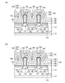
第1実施形態による半導体装置の製造方法を図1乃至図5を用いて説明する。図1乃至図4は、本実施形態による半導体装置の製造方法を示す工程断面図である。
次に、本実施形態による半導体装置の製造方法の評価結果について図6乃至図9を用いて説明する。
次に、本実施形態の変形例による半導体装置の製造方法を図10乃至図12を用いて説明する。図10乃至図12は、本実施形態による半導体装置の製造方法を示す工程断面図である。
第2実施形態による半導体装置の製造方法を図13乃至図15を用いて説明する。図13乃至図15は、本実施形態による半導体装置の製造方法を示す工程断面図である。図1乃至図12に示す第1実施形態による半導体装置の製造方法と同一の構成要素には、同一の符号を付して説明を省略または簡潔にする。
第3実施形態による半導体装置の製造方法を図16乃至図19を用いて説明する。図16乃至図19は、本実施形態による半導体装置の製造方法を示す工程断面図である。図1乃至図15に示す第1又は第2実施形態による半導体装置の製造方法と同一の構成要素には、同一の符号を付して説明を省略または簡潔にする。
第4実施形態による半導体装置の製造方法を図20乃至図25を用いて説明する。図20乃至図25は、本実施形態による半導体装置の製造方法を示す工程断面図である。図1乃至図19に示す第1乃至第3実施形態による半導体装置の製造方法と同一の構成要素には、同一の符号を付して説明を省略または簡潔にする。
次に、本実施形態の変形例による半導体装置の製造方法を図26乃至図29を用いて説明する。図26乃至図29は、本実施形態による半導体装置の製造方法を示す工程断面図である。
第5実施形態による半導体装置の製造方法を図30乃至図33を用いて説明する。図30乃至図33は、本実施形態による半導体装置の製造方法を示す工程断面図である。図1乃至図29に示す第1乃至第4実施形態による半導体装置の製造方法と同一の構成要素には、同一の符号を付して説明を省略または簡潔にする。
第6実施形態による半導体装置の製造方法を図34乃至図38を用いて説明する。図34乃至図38は、本実施形態による半導体装置の製造方法を示す工程断面図である。図1乃至図33に示す第1乃至第5実施形態による半導体装置の製造方法と同一の構成要素には、同一の符号を付して説明を省略または簡潔にする。
上記実施形態に限らず種々の変形が可能である。
半導体基板にトランジスタを形成する工程と、
前記半導体基板上に、前記トランジスタを覆う第1のシリコン窒化膜を形成する工程と、
前記第1のシリコン窒化膜にNH4Fラジカルを供給する工程と、
前記NH4Fラジカルを供給する工程の後、前記第1のシリコン窒化膜に対して熱処理を行う工程と、
前記熱処理を行う工程の後、前記第1のシリコン窒化膜上に第2のシリコン窒化膜を形成する工程と
を有することを特徴とする半導体装置の製造方法。
付記1記載の半導体装置の製造方法において、
前記第1のシリコン窒化膜を形成する工程の後、前記第1のシリコン窒化膜にNH4Fラジカルを供給する工程の前に、前記第1のシリコン窒化膜に対してプラズマ処理を行う工程を更に有する
ことを特徴とする半導体装置の製造方法。
付記2記載の半導体装置の製造方法において、
前記プラズマ処理を行う工程では、酸素プラズマ処理を行う
ことを特徴とする半導体装置の製造方法。
付記1記載の半導体装置の製造方法において、
前記第1のシリコン窒化膜に対して熱処理を行う工程の後、前記第2のシリコン窒化膜を形成する工程の前に、前記第1のシリコン窒化膜に対して紫外線キュアを行う工程を更に有する
ことを特徴とする半導体装置の製造方法。
付記1乃至4のいずれかに記載の半導体装置の製造方法において、
前記第1のシリコン窒化膜を熱処理する工程の後、前記第2のシリコン窒化膜を形成する工程の前に、前記第1のシリコン窒化膜にNH4Fラジカルを更に供給する工程と、前記第1のシリコン窒化膜に対して更に熱処理を行う工程とを更に有する
ことを特徴とする半導体装置の製造方法。
付記1乃至4のいずれかに記載の半導体装置の製造方法において、
前記第2のシリコン窒化膜を形成する工程の後、前記第2のシリコン窒化膜にNH4Fラジカルを供給する工程と、前記第2のシリコン窒化膜に対して熱処理を行う工程とを更に有する
ことを特徴とする半導体装置の製造方法。
付記1乃至6のいずれかに記載の半導体装置の製造方法において、
前記第1のシリコン窒化膜にNH4Fラジカルを供給する工程では、前記半導体基板から離間した箇所に配されたプラズマ室においてNH4Fラジカルを生成する
ことを特徴とする半導体装置の製造方法。
付記7記載の半導体装置の製造方法において、
前記第1のシリコン窒化膜にNH4Fラジカルを供給する工程では、NF3ガスとNH3ガスとを前記プラズマ室に導入する
ことを特徴とする半導体装置の製造方法。
付記1乃至8のいずれかに記載の半導体装置の製造方法において、
前記第1のシリコン窒化膜に対して熱処理を行う工程では、前記第1のシリコン窒化膜を100℃以上に加熱する
ことを特徴とする半導体装置の製造方法。
付記1乃至9のいずれかに記載の半導体装置の製造方法において、
前記第1のシリコン窒化膜にNH4Fラジカルを供給する工程では、シャワーヘッドを介して前記第1のシリコン窒化膜にNH4Fラジカルを供給し、
前記第1のシリコン窒化膜に対して熱処理を行う工程では、加熱された前記シャワーヘッドと前記第1のシリコン窒化膜とを近接させることにより、前記第1のシリコン窒化膜に対して熱処理を行う
ことを特徴とする半導体装置の製造方法。
付記1乃至10のいずれかに記載の半導体装置の製造方法において、
前記第1のシリコン窒化膜にNH4Fラジカルを供給する工程における前記半導体基板の温度は、室温〜100℃である
ことを特徴とする半導体装置の製造方法。
14…素子分離領域
16…P型ウェル
18…ゲート絶縁膜
20…ゲート電極
22…エクステンション領域
24…シリコン窒化膜
26…シリコン窒化膜
28…サイドウォール絶縁膜
30…不純物拡散領域
32…ソース/ドレイン拡散層
34…シリサイド膜
36…NMOSトランジスタ
37…チャネル領域
38…シリコン窒化膜、引張応力膜
40…シリコン窒化膜、引張応力膜
42…シリコン窒化膜、引張応力膜
44…シリコン窒化膜、引張応力膜
45…積層膜、引張応力膜
46…ステージ
48…リフトピン
50…シャワープレート
52…シャワーヘッド
54…ヒータ
56…プラズマ室
58…N型ウェル
60…エクステンション領域
62…不純物拡散領域
64…ソース/ドレイン拡散層
66…凹部
68…シリコンゲルマニウム層
70…PMOSトランジスタ
71…チャネル領域
72…シリコン窒化膜、圧縮応力膜
74…シリコン窒化膜、圧縮応力膜
76…シリコン窒化膜、圧縮応力膜
78…シリコン窒化膜、圧縮応力膜
79…積層膜、圧縮応力膜
110…半導体基板
114…素子分離領域
116…ウェル
118…ゲート絶縁膜
120…ゲート電極
122…エクステンション領域
124…シリコン酸化膜
126…シリコン窒化膜
128…サイドウォール絶縁膜
130…不純物拡散領域
132…ソース/ドレイン拡散層
134…シリサイド膜
136…トランジスタ
138…シリコン窒化膜
140…シリコン窒化膜
142…シリコン窒化膜
144…シリコン窒化膜
145…鬆
146…応力膜
Claims (10)
- 半導体基板にトランジスタを形成する工程と、
前記半導体基板上に、前記トランジスタを覆う第1のシリコン窒化膜を形成する工程と、
前記第1のシリコン窒化膜を形成する工程の後、プラズマ処理を行う工程と、
前記プラズマ処理を行う工程の後、前記第1のシリコン窒化膜にNH4Fラジカルを供給する工程と、
前記NH4Fラジカルを供給する工程の後、熱処理を行う工程と、
前記熱処理を行う工程の後、前記第1のシリコン窒化膜上に第2のシリコン窒化膜を形成する工程と
を有することを特徴とする半導体装置の製造方法。 - 請求項1記載の半導体装置の製造方法において、
前記プラズマ処理を行う工程では、酸素プラズマ処理を行う
ことを特徴とする半導体装置の製造方法。 - 半導体基板上にゲート電極を有するトランジスタを形成する工程と、
前記トランジスタ上に第1のシリコン窒化膜を形成する工程と、
前記第1のシリコン窒化膜を形成する工程の後、シャワーヘッドを介して第1のNH4Fラジカルを供給する工程と、
前記第1のNH4Fラジカルを供給する工程の後、加熱された前記シャワーヘッドと前記第1のシリコン窒化膜とを近接させることにより、第1の熱処理を行なう工程と、
前記第1の熱処理の後、前記シャワーヘッドを介して第2のNH4Fラジカルを供給する工程と、
前記第2のNH4Fラジカルを供給する工程の後、加熱された前記シャワーヘッドと前記第1のシリコン窒化膜とを近接させることにより、第2の熱処理を行なう工程と、
前記第2の熱処理の後、前記第1のシリコン窒化膜上に第2のシリコン窒化膜を形成する工程と
を有する半導体装置の製造方法。 - 請求項3記載の半導体装置の製造方法において、
前記第1及び第2の熱処理後、前記ゲート電極上に前記第1のシリコン窒化膜が残存している
ことを特徴とする半導体装置の製造方法。 - 請求項3又は4に記載の半導体装置の製造方法において、
前記第1のNH4Fラジカルを供給する工程と、前記第2のNH4Fラジカルを供給する工程との処理時間が等しい
ことを特徴とする半導体装置の製造方法。 - 請求項1又は2記載の半導体装置の製造方法において、
前記NH4Fラジカルを供給する工程では、前記半導体基板から離間した箇所に配されたプラズマ室においてNH4Fラジカルを生成する
ことを特徴とする半導体装置の製造方法。 - 請求項6記載の半導体装置の製造方法において、
前記NH4Fラジカルを供給する工程では、NF3ガスとNH3ガスとを前記プラズマ室に導入する
ことを特徴とする半導体装置の製造方法。 - 請求項1、2、6及び7のいずれか1項に記載の半導体装置の製造方法において、
前記熱処理を行う工程では、前記第1のシリコン窒化膜を100℃以上に加熱する
ことを特徴とする半導体装置の製造方法。 - 請求項3乃至5のいずれか1項に記載の半導体装置の製造方法において、
前記第1の熱処理および前記第2の熱処理を行う工程では、前記第1のシリコン窒化膜を100℃以上に加熱する
ことを特徴とする半導体装置の製造方法。 - 請求項1、2、6、7及び8のいずれか1項に記載の半導体装置の製造方法において、
前記NH4Fラジカルを供給する工程では、シャワーヘッドを介してNH4Fラジカルを供給し、
前記熱処理を行う工程では、加熱された前記シャワーヘッドと前記第1のシリコン窒化膜とを近接させることにより、前記熱処理を行う
ことを特徴とする半導体装置の製造方法。
Priority Applications (2)
| Application Number | Priority Date | Filing Date | Title |
|---|---|---|---|
| JP2010108111A JP5703590B2 (ja) | 2010-05-10 | 2010-05-10 | 半導体装置の製造方法 |
| US13/053,898 US8383524B2 (en) | 2010-05-10 | 2011-03-22 | Semiconductor device manufacturing method |
Applications Claiming Priority (1)
| Application Number | Priority Date | Filing Date | Title |
|---|---|---|---|
| JP2010108111A JP5703590B2 (ja) | 2010-05-10 | 2010-05-10 | 半導体装置の製造方法 |
Publications (2)
| Publication Number | Publication Date |
|---|---|
| JP2011238733A JP2011238733A (ja) | 2011-11-24 |
| JP5703590B2 true JP5703590B2 (ja) | 2015-04-22 |
Family
ID=44902221
Family Applications (1)
| Application Number | Title | Priority Date | Filing Date |
|---|---|---|---|
| JP2010108111A Expired - Fee Related JP5703590B2 (ja) | 2010-05-10 | 2010-05-10 | 半導体装置の製造方法 |
Country Status (2)
| Country | Link |
|---|---|
| US (1) | US8383524B2 (ja) |
| JP (1) | JP5703590B2 (ja) |
Families Citing this family (6)
| Publication number | Priority date | Publication date | Assignee | Title |
|---|---|---|---|---|
| JP6097192B2 (ja) | 2013-04-19 | 2017-03-15 | 東京エレクトロン株式会社 | エッチング方法 |
| US8980758B1 (en) * | 2013-09-17 | 2015-03-17 | Applied Materials, Inc. | Methods for etching an etching stop layer utilizing a cyclical etching process |
| JP5971870B2 (ja) * | 2013-11-29 | 2016-08-17 | 株式会社日立国際電気 | 基板処理装置、半導体装置の製造方法及び記録媒体 |
| US9299577B2 (en) * | 2014-01-24 | 2016-03-29 | Applied Materials, Inc. | Methods for etching a dielectric barrier layer in a dual damascene structure |
| KR102003361B1 (ko) * | 2017-09-19 | 2019-07-24 | 무진전자 주식회사 | 인시튜 건식 세정 방법 및 장치 |
| KR101981738B1 (ko) * | 2017-09-19 | 2019-05-27 | 무진전자 주식회사 | 기판 처리 방법 및 장치 |
Family Cites Families (7)
| Publication number | Priority date | Publication date | Assignee | Title |
|---|---|---|---|---|
| JPH05190540A (ja) | 1992-01-13 | 1993-07-30 | Kawasaki Steel Corp | 表面保護膜の形成方法 |
| JPH07106325A (ja) | 1993-09-30 | 1995-04-21 | Sony Corp | 半導体装置の製造方法 |
| US20080142483A1 (en) * | 2006-12-07 | 2008-06-19 | Applied Materials, Inc. | Multi-step dep-etch-dep high density plasma chemical vapor deposition processes for dielectric gapfills |
| JP2009140944A (ja) * | 2007-12-03 | 2009-06-25 | Toshiba Corp | 酸化膜エッチング方法 |
| JP2009224527A (ja) * | 2008-03-17 | 2009-10-01 | Nano Material Kenkyusho:Kk | 半導体デバイス、半導体製造装置及び半導体製造方法 |
| JP2009277849A (ja) * | 2008-05-14 | 2009-11-26 | Toshiba Corp | 半導体装置及びその製造方法 |
| US7994002B2 (en) * | 2008-11-24 | 2011-08-09 | Applied Materials, Inc. | Method and apparatus for trench and via profile modification |
-
2010
- 2010-05-10 JP JP2010108111A patent/JP5703590B2/ja not_active Expired - Fee Related
-
2011
- 2011-03-22 US US13/053,898 patent/US8383524B2/en not_active Expired - Fee Related
Also Published As
| Publication number | Publication date |
|---|---|
| US8383524B2 (en) | 2013-02-26 |
| JP2011238733A (ja) | 2011-11-24 |
| US20110275225A1 (en) | 2011-11-10 |
Similar Documents
| Publication | Publication Date | Title |
|---|---|---|
| JP5173582B2 (ja) | 半導体装置 | |
| US8598661B2 (en) | Epitaxial process for forming semiconductor devices | |
| JP5003515B2 (ja) | 半導体装置 | |
| CN101894789B (zh) | 隔离结构的制造方法 | |
| JP5703590B2 (ja) | 半導体装置の製造方法 | |
| JP2008244059A (ja) | 半導体装置の製造方法 | |
| US20090236664A1 (en) | Integration scheme for constrained seg growth on poly during raised s/d processing | |
| JP5547877B2 (ja) | 半導体装置およびその製造方法 | |
| JP2000323711A (ja) | 半導体素子の製造方法 | |
| JP6083150B2 (ja) | 半導体装置の製造方法 | |
| KR100781549B1 (ko) | 반도체 집적 회로 장치의 제조 방법 및 그에 의해 제조된반도체 집적 회로 장치 | |
| US8993418B2 (en) | Shallow heavily doped semiconductor layer by cyclic selective epitaxial deposition process | |
| JP2011187498A (ja) | 半導体装置の製造方法 | |
| US20110001197A1 (en) | Method for manufacturing semiconductor device and semiconductor device | |
| CN105826199A (zh) | 半导体结构的形成方法 | |
| JP5119604B2 (ja) | 半導体装置の製造方法 | |
| CN102832129B (zh) | 一种半导体器件的制造方法 | |
| CN100401530C (zh) | 形成应变沟道元件的方法 | |
| CN101197282A (zh) | 半导体器件及其制造方法 | |
| TWI828907B (zh) | 半導體製程 | |
| WO2009104507A1 (ja) | 薄膜およびその薄膜を用いた半導体装置の製造方法 | |
| KR100606924B1 (ko) | 반도체 소자의 제조방법 | |
| JP4795028B2 (ja) | 不純物が除去されたシリコン窒化膜を備える半導体素子の製造方法 | |
| JP2000299463A (ja) | 半導体装置の製造方法 | |
| JP5387700B2 (ja) | 半導体装置の製造方法 |
Legal Events
| Date | Code | Title | Description |
|---|---|---|---|
| A621 | Written request for application examination |
Free format text: JAPANESE INTERMEDIATE CODE: A621 Effective date: 20130129 |
|
| RD04 | Notification of resignation of power of attorney |
Free format text: JAPANESE INTERMEDIATE CODE: A7424 Effective date: 20131028 |
|
| A131 | Notification of reasons for refusal |
Free format text: JAPANESE INTERMEDIATE CODE: A131 Effective date: 20140128 |
|
| A977 | Report on retrieval |
Free format text: JAPANESE INTERMEDIATE CODE: A971007 Effective date: 20140131 |
|
| A521 | Request for written amendment filed |
Free format text: JAPANESE INTERMEDIATE CODE: A523 Effective date: 20140328 |
|
| A131 | Notification of reasons for refusal |
Free format text: JAPANESE INTERMEDIATE CODE: A131 Effective date: 20141028 |
|
| A521 | Request for written amendment filed |
Free format text: JAPANESE INTERMEDIATE CODE: A523 Effective date: 20150105 |
|
| TRDD | Decision of grant or rejection written | ||
| A01 | Written decision to grant a patent or to grant a registration (utility model) |
Free format text: JAPANESE INTERMEDIATE CODE: A01 Effective date: 20150127 |
|
| A61 | First payment of annual fees (during grant procedure) |
Free format text: JAPANESE INTERMEDIATE CODE: A61 Effective date: 20150209 |
|
| R150 | Certificate of patent or registration of utility model |
Ref document number: 5703590 Country of ref document: JP Free format text: JAPANESE INTERMEDIATE CODE: R150 |
|
| S531 | Written request for registration of change of domicile |
Free format text: JAPANESE INTERMEDIATE CODE: R313531 |
|
| R350 | Written notification of registration of transfer |
Free format text: JAPANESE INTERMEDIATE CODE: R350 |
|
| LAPS | Cancellation because of no payment of annual fees |