JP5732014B2 - Doherty amplifier - Google Patents
Doherty amplifier Download PDFInfo
- Publication number
- JP5732014B2 JP5732014B2 JP2012207156A JP2012207156A JP5732014B2 JP 5732014 B2 JP5732014 B2 JP 5732014B2 JP 2012207156 A JP2012207156 A JP 2012207156A JP 2012207156 A JP2012207156 A JP 2012207156A JP 5732014 B2 JP5732014 B2 JP 5732014B2
- Authority
- JP
- Japan
- Prior art keywords
- amplifier
- transformer
- phase
- peak
- signal
- Prior art date
- Legal status (The legal status is an assumption and is not a legal conclusion. Google has not performed a legal analysis and makes no representation as to the accuracy of the status listed.)
- Active
Links
- 230000001934 delay Effects 0.000 claims description 6
- 238000010586 diagram Methods 0.000 description 25
- 230000008878 coupling Effects 0.000 description 4
- 238000010168 coupling process Methods 0.000 description 4
- 238000005859 coupling reaction Methods 0.000 description 4
- 230000006872 improvement Effects 0.000 description 4
- 230000003321 amplification Effects 0.000 description 3
- 238000003199 nucleic acid amplification method Methods 0.000 description 3
- 239000003990 capacitor Substances 0.000 description 2
- 230000007423 decrease Effects 0.000 description 2
- 230000003247 decreasing effect Effects 0.000 description 2
- 238000001514 detection method Methods 0.000 description 2
- 238000000034 method Methods 0.000 description 2
- 230000003071 parasitic effect Effects 0.000 description 2
- 238000004088 simulation Methods 0.000 description 2
- 238000013459 approach Methods 0.000 description 1
- 230000005540 biological transmission Effects 0.000 description 1
- 230000008859 change Effects 0.000 description 1
- 238000011161 development Methods 0.000 description 1
- 230000000694 effects Effects 0.000 description 1
- 239000002360 explosive Substances 0.000 description 1
- 238000003780 insertion Methods 0.000 description 1
- 230000037431 insertion Effects 0.000 description 1
- 238000010295 mobile communication Methods 0.000 description 1
- 230000009467 reduction Effects 0.000 description 1
- 230000002040 relaxant effect Effects 0.000 description 1
- 238000012360 testing method Methods 0.000 description 1
- 238000011144 upstream manufacturing Methods 0.000 description 1
Images






Landscapes
- Amplifiers (AREA)
Description
本発明は、高周波用の電力増幅器としてのドハティ増幅器に関し、より詳細には、増幅器をトランスで接続してその同調周波数を調整することにより、トランスの1次側・2次側の同調周波数をずらして増幅器の広帯域化を図りようにしたドハティ増幅器に関する。 The present invention relates to a Doherty amplifier as a high-frequency power amplifier. More specifically, the tuning frequency of the primary side and the secondary side of the transformer is shifted by connecting the amplifiers with a transformer and adjusting the tuning frequency. The present invention relates to a Doherty amplifier designed to increase the bandwidth of the amplifier.
近年、移動体通信や無線LAN(Local Area Network)などの進歩は著しく、特に、携帯電話の爆発的な普及と、それに伴うインフラ整備により、携帯端末のみならず基地局にも低消費電力化が要求されてきている。そこで、基地局において送信に使用される増幅器についても、効率及び線形性の向上に対する要求が一層高まってきている。 In recent years, mobile communication and wireless LAN (Local Area Network) have made remarkable progress. In particular, the explosive spread of mobile phones and the accompanying infrastructure development have reduced power consumption not only for mobile terminals but also for base stations. It has been requested. Therefore, there is an increasing demand for an improvement in efficiency and linearity for amplifiers used for transmission in base stations.
しかしながら、一般的な増幅器では、効率と線形性との間にはトレードオフの関係があり、また、効率は増幅器への入力レベルに比例する。したがって、高い効率は、増幅器の出力が最大出力電力に近づくまで得られないので、増幅器の線形性を実現することは難しい。そこで、ドハティ増幅器(Doherty Amplifier)などのような高効率で信号を増幅する技術と、その低歪化やフィードフォワード等の歪補償技術とを組み合わせることにより、より高効率で低歪な増幅器が開発されている。このドハティ増幅器は、基本的にAB級のキャリア増幅器とC級のピーク増幅器を組み合わせ、これらの増幅器の出力を合成して高効率の増幅を実現するものである。 However, in a typical amplifier, there is a trade-off between efficiency and linearity, and efficiency is proportional to the input level to the amplifier. Therefore, high efficiency is not obtained until the amplifier output approaches the maximum output power, so it is difficult to achieve amplifier linearity. Therefore, a high-efficiency, low-distortion amplifier has been developed by combining high-efficiency signal amplification techniques such as Doherty Amplifiers with distortion compensation techniques such as low distortion and feedforward. Has been. This Doherty amplifier basically combines a class AB carrier amplifier and a class C peak amplifier, and combines the outputs of these amplifiers to realize high efficiency amplification.
図1は、従来のエミッタ増幅器を用いたドハティ増幅器を説明するための回路構成図で、図中符号1は分配器、2はメイン増幅器(キャリア増幅器)、3はピーク増幅器、4,5は90°移相器を示している。この従来のドハティ増幅器は、入力信号を2つの入力信号に分配する分配器1と、この分配器1の出力信号が直接入力されるメイン増幅器2と、分配器1の出力位相を90°遅らせる第1の90°移相器4と、この第1の90°移相器4の出力信号を入力信号とするピーク増幅器3と、メイン増幅器2の出力位相を90°移相させる第2の90°移相器5とで構成され、ピーク増幅器3の出力と第2の90°移相器5の出力が、同相となることを利用して高効率を達成する回路構成図である。この図1に示したドハティ増幅器において、メイン増幅器2とピーク増幅器3との各々は、電流を出力し、負荷抵抗Rによって加算されて電圧に変換されて出力される。
FIG. 1 is a circuit diagram for explaining a Doherty amplifier using a conventional emitter amplifier. In FIG. 1,
図2(a),(b)は、非特許文献1に開示されているドハティ増幅器を説明するための回路構成図で、図2(a)はドハティ増幅器の利得低下を説明するための回路構成図、図2(b)は図2(a)のピーク増幅器の等価回路を示す図である。
メイン増幅器2の出力は、第2の90°移相器5を経由する必要があるため、ピーク増幅器3のバース電流と逆相となり、ピーク増幅器3の効率を低下させる様子が開示されている。
2A and 2B are circuit configuration diagrams for explaining the Doherty amplifier disclosed in
Since the output of the
図3は、図2(a),(b)と同様に、非特許文献1に開示されているドハティ増幅器を説明するための回路構成図である。ピーク増幅器3のベース電流をメイン増幅器2の出力成分が打ち消されないようにするために、メイン増幅器2の入力と分配器1との間に可変位相器6を挿入することが開示されている。
FIG. 3 is a circuit configuration diagram for explaining the Doherty amplifier disclosed in
また、例えば、特許文献1に記載のものは、高周波帯域において変調波信号を増幅するための高出力増幅器に関するもので、特に、バックオフが大きな動作状態においても効率の高い高出力増幅器を実現するドハティ型増幅器に関するものである。この特許文献1のものは、可変減衰器及び可変移相器をピーク増幅器の入力側に設けたもので、ピーク増幅器の入力側に配置される可変減衰器及びピーク増幅器の入力側に配置される可変移相器を備えるようにしたので、キャリア増幅器とピーク増幅器との利得の差及び通過位相量の差を補償して、出力端におけるキャリア増幅器の出力電力とピーク増幅器の出力電力との合成を良好に実施することができ、マイクロ波ドハティ型増幅器全体としての出力電力や効率を向上することができるというものである。
Further, for example, the one described in
しかしながら、近年、レーダ・移動体検知の用途では、最大検知距離実現のために高出力を広い周囲条件範囲にわたって一定に保つことが求められている。上述したような従来技術では、増幅度がメイン増幅器からピーク増幅器への回り込みで低下するという問題や、メイン増幅器とピーク増幅器のバイアス条件が異なるために位相差が生じるという問題や、さらには、メイン増幅器とピーク増幅器との位相干渉によって3次相互変調歪が劣化するというような問題がある。 However, in recent years, in radar / moving object detection, it has been required to keep a high output constant over a wide range of ambient conditions in order to realize a maximum detection distance. In the prior art as described above, the amplification level decreases due to the wraparound from the main amplifier to the peak amplifier, the phase difference occurs because the bias conditions of the main amplifier and the peak amplifier are different, and further, There is a problem that third-order intermodulation distortion deteriorates due to phase interference between the amplifier and the peak amplifier.
本発明は、このような問題に鑑みてなされたもので、その目的とするところは、増幅器をトランスで接続してその同調周波数を調整することにより、トランスの1次側・2次側の同調周波数をずらして増幅器の広帯域化を図るようにしたドハティ増幅器を提供することにある。 The present invention has been made in view of such problems. The object of the present invention is to tune the primary side and the secondary side of the transformer by connecting an amplifier with a transformer and adjusting the tuning frequency. It is an object of the present invention to provide a Doherty amplifier in which the frequency is shifted to increase the bandwidth of the amplifier.
本発明は、このような目的を達成するためになされたもので、請求項1に記載の発明は、入力信号が分配される分配器と、該分配器からの分配された一方の信号が入力されるメイン増幅器と、前記分配器からの分配された他方の信号の位相を90度遅らせる第1の移相器と、該第1の移相器からの信号が入力されるピーク増幅器と、前記メイン増幅器からの信号の位相を90度遅らせる第2の移相器と、前記ピーク増幅器からの信号と前記第2の移相器からの信号を加算する加算器とを備え、前記メイン増幅器及び前記ピーク増幅器の少なくとも一方は、第1の差動対を含む第1の増幅部と、前記第1の差動対の負荷である1次側トランス及び前記1次側トランスと対になる2次側トランスを含む第1のトランス部と、前記2次側トランスが接続される第2の差動対を含む第2の増幅器と、を備え、前記メイン増幅器及び前記ピーク増幅器の少なくとも一方からの信号の位相を可変にする位相制御信号を用いて、前記1次側トランス及び前記2次側トランスが有する負荷の少なくとも一方を可変とすることを特徴とする。
The present invention has been made to achieve such an object. The invention according to
また、請求項2に記載の発明は、請求項1に記載の発明において、前記メイン増幅器及び前記ピーク増幅器の少なくとも一方は、前記第1の増幅器の前段に接続され、1次側トランス及び前記1次側トランスと対になる2次側トランスを含む第2のトランス部とをさらに備えていることを特徴とする。
Also, an invention according to
また、請求項3に記載の発明は、請求項1に記載の発明において、前記メイン増幅器及びピーク増幅器の少なくとも一方は、前記第2の増幅器の差動対の負荷である1次側トランス及び前記1次側トランスと対になる2次側トランスを含む第3のトランス部とを備えていることを特徴とする。
また、請求項4に記載の発明は、請求項1乃至3のいずれかに記載の発明において、前記1次側トランス及び前記2次側トランスが有する負荷は、可変容量素子であることを特徴とする。
The invention according to
The invention according to claim 4 is the invention according to any one of
本発明によれば、増幅器をトランスで接続してその同調周波数を調整することにより、トランスの1次側・2次側の同調周波数をずらして増幅器の広帯域化を図りようにしたドハティ増幅器を実現することができる。また、トランスの1次側・2次側の同調周波数をずらして設計することで、増幅器の広帯域化も同時に達成できる。また、複数のトランスの同調周波数をずらして設計することで、増幅器の広帯域化も同時に達成できる。また、カスコード中間ノードの寄生容量を緩和することで、寄生のPoleを高周波側に移動させ、広帯域化を同時に達成することができる。さらに、ドハティ増幅器は、通常、メイン増幅器をClassAB、ピーク増幅器をClassCで実現することができるという効果を奏する。 According to the present invention, a Doherty amplifier is realized in which the tuning frequency of the primary side and the secondary side of the transformer is shifted to increase the bandwidth of the amplifier by connecting the amplifier with a transformer and adjusting the tuning frequency. can do. Further, by designing the transformer so that the tuning frequencies on the primary and secondary sides of the transformer are shifted, it is possible to simultaneously achieve a wide band of the amplifier. In addition, by designing the plurality of transformers with different tuning frequencies, it is possible to simultaneously achieve a wide band of amplifiers. Further, by relaxing the parasitic capacitance of the cascode intermediate node, the parasitic pole can be moved to the high frequency side, and a wide band can be achieved at the same time. Furthermore, the Doherty amplifier usually has an effect that the main amplifier can be realized by Class AB and the peak amplifier can be realized by Class C.
以下、図面を参照して本発明の実施の形態について説明する。
図4は、本発明に係るドハティ増幅器の実施形態を説明するための回路構成図である。図中符号11は分配器、12はメイン増幅器(トランス付)、13はピーク増幅器(トランス付)、14は第1の90°移相器、15は第2の90°移相器、16は加算器を示している。
Embodiments of the present invention will be described below with reference to the drawings.
FIG. 4 is a circuit configuration diagram for explaining an embodiment of the Doherty amplifier according to the present invention. In the figure, 11 is a distributor, 12 is a main amplifier (with transformer), 13 is a peak amplifier (with transformer), 14 is a first 90 ° phase shifter, 15 is a second 90 ° phase shifter, and 16 is An adder is shown.
本実施形態におけるドハティ増幅器は、上述した非特許文献1のような新たな回路を追加することなく位相可変を実現した。トランス間負荷非対称性に起因した回路は、1)新たな素子挿入がないので、回路損失が最小である。2)10GHz以上では一般的にQL>QCなので、DC−Cut容量を付加するより、Transを用いてAC結合を実現する方が損失が少ない。3)高周波ではL自身も小さくない回路規模の縮小が期待できる。
The Doherty amplifier according to the present embodiment realizes variable phase without adding a new circuit as in
このことを、図4に基づいて説明する。
図4に示した高線形ドハティ増幅器は、入力信号が分配される分配器11と、この分配器11からの分配された一方の信号が入力されるメイン増幅器12と、分配器11からの分配された他方の信号の位相を90度遅らせる第1の移相器14と、この第1の移相器14からの信号が入力されるピーク増幅器13と、メイン増幅器12からの信号の位相を90度遅らせる第2の移相器15と、ピーク増幅器13からの信号と第2の移相器15からの信号を加算する加算器16とを備えている。
This will be described with reference to FIG.
The highly linear Doherty amplifier shown in FIG. 4 includes a distributor 11 to which an input signal is distributed, a
メイン増幅器12とピーク増幅器13は、それぞれトランスと増幅器とで構成され、1次と2次のトランス負荷が異なることを利用して、メイン増幅器12とピーク増幅器13との間に位相差を生じさせるものである。
The
図5は、図4に示したメイン増幅器及びピーク増幅器の具体的な実施例1を示す回路構成図である。図中符号20は第1のトランス部、21は差動負荷トランス(1次側)、22は差動負荷トランス(2次側)、23は差動対増幅器を示している。
本実施例1は、メイン増幅器12及びピーク増幅器13の少なくとも一方は、差動対を含む第1の増幅部23と、差動対の負荷である1次側トランス21及び1次側トランス21と対になる2次側トランス22を含む第1のトランス部20とを備え、1次側トランス21及び2次側トランス22が有する負荷の少なくとも一方を可変とする。
FIG. 5 is a circuit configuration diagram showing a specific example 1 of the main amplifier and the peak amplifier shown in FIG. In the figure,
In the first embodiment, at least one of the
つまり、図5における差動対増幅部23は、差動対を入力し、負荷部には、トランスの1次側が実装され、トランスの2次側は出力端子となっている。トランスの1次側と2次側の結合係数はkで、第1のトランス部20の負荷を位相制御信号を用いて可変にすることで差動出力位相を変化させることができる。
図6(a),(b)は、トランスの1次側と2次側のそれぞれをLCR並列回路で表した図で、図6(a)は、メイン増幅器及びピーク増幅器の1次側モデル、図6(b)は、シミュレーションのテスト回路を示す図である。なお、図6(a)におけるLCR並列回路は、図6(b)におけるそれぞれにLCR回路に相当している。図6(b)におけるLCR_Lはメイン増幅器の2次側、LCR_Mはメイン増幅器とピーク増幅器の1次側、LCR_Hはピーク増幅器の2次側を示している。LCR_LとLCR_MとLCR_Hを模擬して利得を変えることなく位相を可変できることを示している。
That is, the differential
6A and 6B are diagrams showing the primary side and the secondary side of the transformer as LCR parallel circuits, respectively, and FIG. 6A shows the primary side models of the main amplifier and the peak amplifier, FIG. 6B is a diagram illustrating a simulation test circuit. Note that the LCR parallel circuit in FIG. 6A corresponds to the LCR circuit in FIG. In FIG. 6B, LCR_L indicates the secondary side of the main amplifier, LCR_M indicates the primary side of the main amplifier and the peak amplifier, and LCR_H indicates the secondary side of the peak amplifier. LCR_L, LCR_M, and LCR_H are simulated to indicate that the phase can be varied without changing the gain.
図6(a),(b)においては、負荷が1次側と2次側で並列接続されるモデルを用いている。1次側の負荷は、メイン増幅器とピーク増幅器が共通であり、2次側の負荷は、メイン増幅器が4×1次側、ピーク増幅器が1/4×1次側である。メイン増幅器とピーク増幅器の1次側と2次側の負荷条件は、表1に示してある。 6A and 6B, a model is used in which the load is connected in parallel on the primary side and the secondary side. The primary side load is common to the main amplifier and the peak amplifier, and the secondary side load is the 4 × primary side of the main amplifier and the 1/4 × primary side of the peak amplifier. The primary and secondary load conditions of the main and peak amplifiers are shown in Table 1.
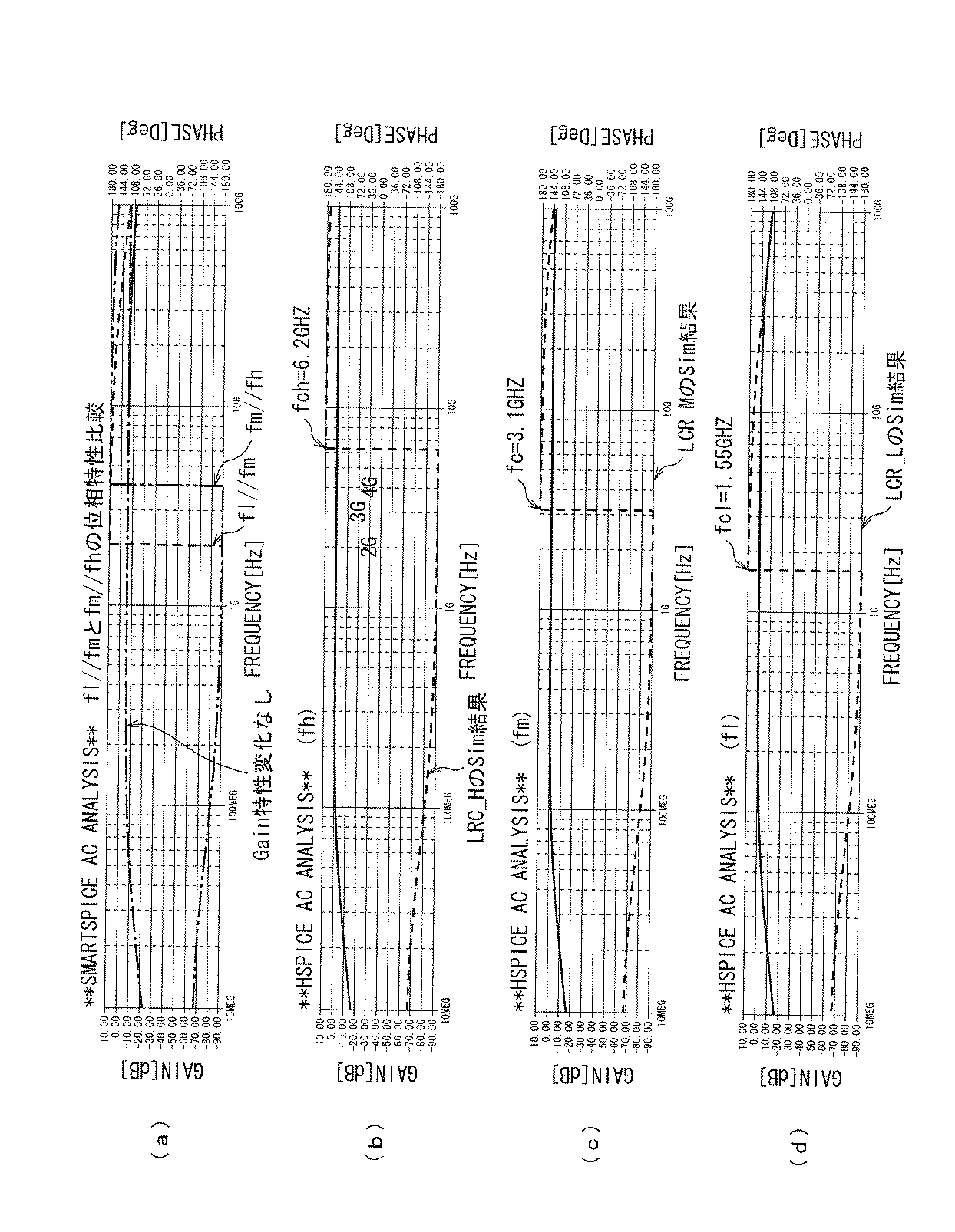
図7(a)乃至(d)は、メイン増幅器とピーク増幅器のパスの利得・位相周波数特性を示す図で、位相・利得変化の様子をシミュレーションで確認した図である。図7(a)は、総合特性であるメイン増幅器対ピーク増幅器間の位相180°で周波数が2GHzほど異なることが確認できた図で、図7(b)は、LCR_H単体の信号結果を示す図で、図7(c)は、LCR_M単体の信号結果を示す図で図7(d)は、LCR_L単体の総合(Sim)結果を示す図である。 FIGS. 7A to 7D are diagrams showing the gain / phase frequency characteristics of the main amplifier and the peak amplifier, and the state of the phase / gain change is confirmed by simulation. FIG. 7A is a diagram showing that the frequency is different by about 2 GHz at a phase of 180 ° between the main amplifier and the peak amplifier, which is a general characteristic, and FIG. 7B is a diagram showing a signal result of LCR_H alone. FIG. 7C is a diagram showing a signal result of LCR_M alone, and FIG. 7D is a diagram showing an overall (Sim) result of LCR_L alone.
図中、fl(エル)はメイン増幅器の2次側、fmはメイン増幅器とピーク増幅器の1次側、fhはピーク増幅器の2次側を示している。また、N1PH(破線)fl/fmはメイン増幅器のパスの位相特性、N2PH(一点鎖線)fm/fhはピーク増幅器のパスの位相特性を示している。
図8乃至図11は、図7(a)乃至(d)に「それぞれ対応した拡大図である。つまり、図8は図7(a)の拡大図、図9は図7(b)の拡大図、図10は図7(c)の拡大図、図11は図7(d)の拡大図である。
In the figure, fl is a secondary side of the main amplifier, fm is a primary side of the main amplifier and the peak amplifier, and fh is a secondary side of the peak amplifier. N1PH (dashed line) fl / fm indicates the phase characteristic of the main amplifier path, and N2PH (one-dot chain line) fm / fh indicates the phase characteristic of the peak amplifier path.
8 to 11 are enlarged views corresponding respectively to FIGS. 7A to 7D. That is, FIG. 8 is an enlarged view of FIG. 7A, and FIG. 9 is an enlarged view of FIG. 7B. 10 and 10 are enlarged views of FIG. 7C, and FIG. 11 is an enlarged view of FIG. 7D.
図中のN1DB(実線)はメイン増幅器の利得特性、N1PH(破線)はメイン増幅器の位相特性、N2DB(一点鎖線)はピーク増幅器の利得特性、N2PH(二点鎖線)はピーク増幅器の位相特性を示している。 In the figure, N1DB (solid line) is the gain characteristic of the main amplifier, N1PH (dashed line) is the phase characteristic of the main amplifier, N2DB (one-dot chain line) is the gain characteristic of the peak amplifier, and N2PH (two-dot chain line) is the phase characteristic of the peak amplifier. Show.
図12は、図4に示したメイン増幅器及びピーク増幅器の具体的な実施例2を示す回路構成図である。図中符号30は第1のトランス部、31は差動負荷トランス(1次側)、32は差動負荷トランス(2次側)、33は第1の差動対増幅器、34は第1の増幅器、35は第2の負荷、36は第2の差動対増幅器、37は第2の増幅器を示している。
本実施例2では、メイン増幅器12及びピーク増幅器13の少なくとも一方は、2次側トランス32が接続される第2の差動対増幅器36を含む第2の増幅器37をさらに備えている。
FIG. 12 is a circuit configuration diagram showing a specific example 2 of the main amplifier and the peak amplifier shown in FIG. In the figure,
In the second embodiment, at least one of the
本実施例2は、増幅器を縦続接続させた場合を示し、本実施例2の実施に際しては、図12に示した回路構成図をメイン増幅器とピーク増幅器の少なくともどちらか一方に用いて、メイン増幅器のパスとピーク増幅器のパスとの間の位相差を調整することが必要である。
入力は、第1の増幅器34の入力部を構成する第1の差動対増幅器33に入力され、第1の増幅器34の第1の負荷へ出力される。第1の負荷はトランスの1次側として構成され、2次側は第2の増幅器37の入力である第2の差動対増幅器36に接続されている。第2の増幅器37は、第2の差動対増幅器36と第2の負荷35とで構成され、第2の差動対増幅器36と第2の負荷35との接続端子が出力として外部との接続に用いている。
The second embodiment shows a case where the amplifiers are connected in cascade. In the second embodiment, the circuit configuration diagram shown in FIG. 12 is used for at least one of the main amplifier and the peak amplifier. It is necessary to adjust the phase difference between the current path and the peak amplifier path.
The input is input to the first
位相制御信号は、トランスの1次側のみに印加される。トランスの2次側の可変容量C2PとC2Nには同一電圧が印加される。トランスの1次側の可変容量はVCIP≠VCIN VCIPはC1Pの位相制御信号、VCINはC1Nの位相制御信号である。C1PとC1NのC−V特性は等しく、かつ電圧に比例して容量値が増えるものとする。P1NとN1Nとの位相差は180°で、いわゆる差動信号が入力される。L1P=L1N=L2P=L2N=Lとする。 The phase control signal is applied only to the primary side of the transformer. The same voltage is applied to the variable capacitors C 2P and C 2N on the secondary side of the transformer. The variable capacity on the primary side of the transformer is V CIP ≠ V CIN V CIP is a C 1P phase control signal, and V CIN is a C 1N phase control signal. It is assumed that the CV characteristics of C 1P and C 1N are equal and the capacitance value increases in proportion to the voltage. The phase difference between P 1N and N 1N is 180 °, and so-called differential signals are input. Let L 1P = L 1N = L 2P = L 2N = L.
VCIP=VCINの時、V1PとV1N、さらにはV2PとV2Nの位相差は180°で、差動増幅器の縦続接続の動作を行う。
VCIP>VCINの時、L1P・C1P>L1P・C1Pとなり、V1P側の位相は“位相遅れ増”、V1N側の位相は“位相遅れ減”の関係を保持したまま、ピーク増幅器の入力に至る。元来、180°の位相差があったため、ピーク増幅器のベース入力に大きく干渉し、線形性、利得を劣化させていたが、位相差≠180°となり、線形性・利得ともに改善される。
When V CIP = V CIN , the phase difference between V 1P and V 1N , and further V 2P and V 2N is 180 °, and the differential amplifiers are connected in cascade.
When V CIP > V CIN , L 1P · C 1P > L 1P · C 1P , the phase on the V 1P side is “increase in phase lag”, and the phase on the V 1N side is kept in the relationship “decrease in phase lag”. To the input of the peak amplifier. Originally, there was a phase difference of 180 °, so that it greatly interfered with the base input of the peak amplifier and deteriorated linearity and gain. However, the phase difference ≠ 180 °, and both linearity and gain were improved.
VCIP<VCINの時、L1P・C1P<L1P・C1Pとなる。このときもVCIP>VCINの時と同様に、位相差180°の関係が崩れているため、線形性・利得が改善される。
以下に、L1P=L1N=L2P=L2N=Lとして説明する。トランスの1次側は、L1PとL1Nの縦続接続、C1PとC1Nの縦続接続が並列配置され、C1PとC1Nは位相制御信号によって容量値が増減できるようになっている。トランスの2次側も、1次側と同様の構成で、1次側と2次側間の結合係数はkである。
When V CIP <V CIN , L 1P · C 1P <L 1P · C 1P . At this time, as in the case of V CIP > V CIN , the relationship of the phase difference of 180 ° is broken, so that the linearity / gain is improved.
Below, it demonstrates as L1P = L1N = L2P = L2N = L. On the primary side of the transformer, cascade connection of L 1P and L 1N and cascade connection of C 1P and C 1N are arranged in parallel, and the capacitance value of C 1P and C 1N can be increased or decreased by a phase control signal. The secondary side of the transformer has the same configuration as the primary side, and the coupling coefficient between the primary side and the secondary side is k.
このような構成の増幅器のC1PとC1N又はC2PとC2Nの少なくともいずれか一方の容量を変化させることで増幅器の位相を変化させる。
つまり、図12に示した本実施例2の構成では、増幅器をメイン増幅器又はピーク増幅器の少なくともどちらか一方に用いて、メイン増幅器の系(パス)とピーク増幅器の系(パス)との間の位相差を発生/調整させ、図2に示したメイン増幅器の信号がピーク増幅器のベース電流を抑圧することを軽減させ、ドハティ増幅器の線形性を向上させる。また、ピーク増幅器のベース信号レベルが低下するのを防止しているとみなすことができるので、ドハティ増幅器の利得・出力パワーの向上にも寄与する。
The phase of the amplifier is changed by changing the capacitance of at least one of C 1P and C 1N or C 2P and C 2N of the amplifier having such a configuration.
That is, in the configuration of the second embodiment shown in FIG. 12, the amplifier is used as at least one of the main amplifier and the peak amplifier, and the system is connected between the main amplifier system (path) and the peak amplifier system (path). A phase difference is generated / adjusted, and the main amplifier signal shown in FIG. 2 is reduced from suppressing the base current of the peak amplifier, thereby improving the linearity of the Doherty amplifier. Further, since it can be considered that the base signal level of the peak amplifier is prevented from being lowered, it contributes to the improvement of the gain and output power of the Doherty amplifier.
図13は、図4に示したメイン増幅器及びピーク増幅器の具体的な実施例3を示す回路構成図である。図中符号40は第1のトランス部、41は差動負荷トランス(1次側)、42は差動負荷トランス(2次側)、43は第1の差動対増幅器、44は第1の増幅器、45は第2のトランス部、46は差動負荷トランス(1次側)、47は差動負荷トランス(2次側)、48は第2の差動対増幅器、49は第2の増幅器、50は第3のトランス部、51は差動負荷トランス(1次側)、52は差動負荷トランス(2次側)を示している。
FIG. 13 is a circuit configuration diagram showing a specific example 3 of the main amplifier and the peak amplifier shown in FIG. In the figure,
メイン増幅器12及びピーク増幅器13の少なくとも一方は、第1の増幅器44の前段に接続され、1次側トランス46及び1次側トランス46と対になる2次側トランス47を含む第2のトランス部45とをさらに備えている。
また、メイン増幅器12及びピーク増幅器13の少なくとも一方は、第2の増幅器49の差動対の負荷である1次側トランス51及び1次側トランス51と対になる2次側トランス52を含む第3のトランス部50とを備えている。
At least one of the
At least one of the
本実施例3は、増幅器を2つの縦続接続させた場合を示し、本実施例3の実施に際しては、図13に示した回路構成図をメイン増幅器とピーク増幅器の少なくともどちらか一方に用いて、メイン増幅器のパスとピーク増幅器のパスとの間の位相差を調整することが必要である。
入力は、第1の増幅器44の入力部を構成する第1のトランス部40を経由して第1の差動対増幅器43に入力され、第1の増幅器44の第1の負荷46が1次側を構成している第2のトランス部45を経由して第2の差動対増幅器48に入力され、さらに、増幅された後に、第2の増幅器49の第2の負荷51が1次側を構成している第3のトランス50を経由して出力される。
The third embodiment shows a case where two amplifiers are connected in cascade. In the implementation of the third embodiment, the circuit configuration diagram shown in FIG. 13 is used for at least one of the main amplifier and the peak amplifier. It is necessary to adjust the phase difference between the main amplifier path and the peak amplifier path.
The input is input to the first
以下に、L1P=L1N=L2P=L2N=L3P=L3N=L4P=L4N=L5P=L5N=L6P=L6N=Lとして説明する。他方、全ての容量素子は可変容量素子で、少なくともその中の1つが位相制御信号によってその容量値が増減される。図13に示している3つのトランスである第1のトランス、第2のトランス、第3のトランスは、その1次側が、LXPとLXNの縦続接続(X=1〜N)、CXPとCXNの縦続接続(X=1〜N)で、LとCは並列配置され、1次側と2次側間の結合係数はkである。また、トランスの2次側の構成は、1次側と相似である。このような構成により、容量を変化させることで増幅器の位相を変化させる。 In the following description, it is assumed that L 1P = L 1N = L 2P = L 2N = L 3P = L 3N = L 4P = L 4N = L 5P = L 5N = L 6P = L 6N = L. On the other hand, all the capacitive elements are variable capacitive elements, and at least one of them is increased or decreased by a phase control signal. The first transformer, the second transformer, and the third transformer, which are the three transformers shown in FIG. 13, are cascaded on the primary side of L XP and L XN (X = 1 to N), C XP And C XN cascade connection (X = 1 to N), L and C are arranged in parallel, and the coupling coefficient between the primary side and the secondary side is k. The configuration of the secondary side of the transformer is similar to the primary side. With such a configuration, the phase of the amplifier is changed by changing the capacitance.
つまり、図13に示した本実施例3の構成では、増幅器をメイン増幅器又はピーク増幅器の少なくともどちらか一方に用いて、メイン増幅器の系(パス)とピーク増幅器の系(パス)との間の位相差を発生/調整させ、図2に示したメイン増幅器の信号がピーク増幅器のベース電流を抑圧することを軽減させ、ドハティ増幅器の線形性を向上させる。また、ピーク増幅器のベース信号レベルが低下するのを防止しているとみなすことができるので、ドハティ増幅器の利得・出力パワーの向上にも寄与する。 That is, in the configuration of the third embodiment shown in FIG. 13, an amplifier is used as at least one of the main amplifier and the peak amplifier, and between the main amplifier system (path) and the peak amplifier system (path). A phase difference is generated / adjusted, and the main amplifier signal shown in FIG. 2 is reduced from suppressing the base current of the peak amplifier, thereby improving the linearity of the Doherty amplifier. Further, since it can be considered that the base signal level of the peak amplifier is prevented from being lowered, it contributes to the improvement of the gain and output power of the Doherty amplifier.
1,11 分配器
2 メイン増幅器(キャリア増幅器)
3 ピーク増幅器
4,5 90°移相器
6 可変位相器
12 メイン増幅器(トランス付)
13 ピーク増幅器(トランス付)
14 第1の90°移相器
15 第2の90°移相器
16 加算器
20,30,40 第1のトランス部
21,31,41,46,51 差動負荷トランス(1次側)
22,32,42,47,52 差動負荷トランス(2次側)
23 差動対増幅器
33,43 第1の差動対増幅器
34,44 第1の増幅器
35 第2の負荷
36,48 第2の差動対増幅器
37,49 第2の増幅器
45 第2のトランス部
50 第3のトランス部
1,11
3 Peak amplifier 4, 5 90 °
13 Peak amplifier (with transformer)
14 First 90 °
22, 32, 42, 47, 52 Differential load transformer (secondary side)
23
Claims (4)
該分配器からの分配された一方の信号が入力されるメイン増幅器と、
前記分配器からの分配された他方の信号の位相を90度遅らせる第1の移相器と、
該第1の移相器からの信号が入力されるピーク増幅器と、
前記メイン増幅器からの信号の位相を90度遅らせる第2の移相器と、
前記ピーク増幅器からの信号と前記第2の移相器からの信号を加算する加算器とを備え、
前記メイン増幅器及び前記ピーク増幅器の少なくとも一方は、第1の差動対を含む第1の増幅部と、前記第1の差動対の負荷である1次側トランス及び前記1次側トランスと対になる2次側トランスを含む第1のトランス部と、前記2次側トランスが接続される第2の差動対を含む第2の増幅器と、を備え、
前記メイン増幅器及び前記ピーク増幅器の少なくとも一方からの信号の位相を可変にする位相制御信号を用いて、前記1次側トランス及び前記2次側トランスが有する負荷の少なくとも一方を可変とすることを特徴とするドハティ増幅器。 A distributor to which the input signal is distributed;
A main amplifier to which one of the distributed signals from the distributor is input;
A first phase shifter that delays the phase of the other distributed signal from the distributor by 90 degrees;
A peak amplifier to which a signal from the first phase shifter is input;
A second phase shifter that delays the phase of the signal from the main amplifier by 90 degrees;
An adder for adding the signal from the peak amplifier and the signal from the second phase shifter;
Wherein at least one of the main amplifier and the peak amplifier includes a first amplifying unit including a first of the differential pair, the first load is a primary transformer and the primary transformer and a pair of differential pairs A first transformer section including a secondary transformer, and a second amplifier including a second differential pair to which the secondary transformer is connected ,
At least one of the loads of the primary transformer and the secondary transformer is made variable using a phase control signal that makes the phase of the signal from at least one of the main amplifier and the peak amplifier variable. Doherty amplifier.
Priority Applications (1)
| Application Number | Priority Date | Filing Date | Title |
|---|---|---|---|
| JP2012207156A JP5732014B2 (en) | 2012-09-20 | 2012-09-20 | Doherty amplifier |
Applications Claiming Priority (1)
| Application Number | Priority Date | Filing Date | Title |
|---|---|---|---|
| JP2012207156A JP5732014B2 (en) | 2012-09-20 | 2012-09-20 | Doherty amplifier |
Publications (2)
| Publication Number | Publication Date |
|---|---|
| JP2014064113A JP2014064113A (en) | 2014-04-10 |
| JP5732014B2 true JP5732014B2 (en) | 2015-06-10 |
Family
ID=50618984
Family Applications (1)
| Application Number | Title | Priority Date | Filing Date |
|---|---|---|---|
| JP2012207156A Active JP5732014B2 (en) | 2012-09-20 | 2012-09-20 | Doherty amplifier |
Country Status (1)
| Country | Link |
|---|---|
| JP (1) | JP5732014B2 (en) |
Families Citing this family (2)
| Publication number | Priority date | Publication date | Assignee | Title |
|---|---|---|---|---|
| CN109067364B (en) * | 2018-06-07 | 2022-04-19 | 佛山市顺德区中山大学研究院 | Doherty power amplifier with broadband and efficient output |
| CN116647199B (en) * | 2023-07-24 | 2023-11-07 | 成都通量科技有限公司 | Tuning transformer and Doherty power amplifier comprising same |
Family Cites Families (5)
| Publication number | Priority date | Publication date | Assignee | Title |
|---|---|---|---|---|
| JPS62278813A (en) * | 1986-05-27 | 1987-12-03 | Clarion Co Ltd | Phase shifter |
| JPH0738368A (en) * | 1993-07-20 | 1995-02-07 | Tdk Corp | 180× phase shifter |
| FR2737821B1 (en) * | 1995-08-09 | 1998-02-13 | Chavanat Paul | DEVICE FOR PHASE-OUT AND PASSIVE AND APERIODIC MITIGATION OF ELECTRICAL SIGNALS |
| JP4467756B2 (en) * | 2000-10-13 | 2010-05-26 | 三菱電機株式会社 | Doherty amplifier |
| JP5541135B2 (en) * | 2010-12-13 | 2014-07-09 | 富士通株式会社 | Amplifier circuit |
-
2012
- 2012-09-20 JP JP2012207156A patent/JP5732014B2/en active Active
Also Published As
| Publication number | Publication date |
|---|---|
| JP2014064113A (en) | 2014-04-10 |
Similar Documents
| Publication | Publication Date | Title |
|---|---|---|
| CN108462477B (en) | Power amplifying circuit | |
| US9748902B2 (en) | Phase correction in a Doherty power amplifier | |
| US8324965B2 (en) | Final stage three-way power combining amplifying circuit applied to power amplifier of mobile communications base station system | |
| CN107210713B (en) | Doherty amplifier | |
| US9899962B2 (en) | Power amplifier | |
| CN112543002B (en) | Broadband differential Doherty power amplifier and its design method and application | |
| CN102113207A (en) | Doherty amplifier with input network optimized for MMIC | |
| WO2023045542A1 (en) | Radio-frequency power amplifier and radio-frequency front-end architecture applied to 5g communication system | |
| JPWO2016113905A1 (en) | Doherty amplifier and power amplifier | |
| CN104218897A (en) | Device and method for providing efficient and compact Doherty power amplifier | |
| JP2009213090A (en) | Power amplification circuit | |
| JPWO2014136402A1 (en) | Mixer circuit | |
| WO2023002778A1 (en) | Power amplification circuit and power amplification method | |
| CN110855247A (en) | E-band multi-channel receiver with vector modulator | |
| WO2023216846A1 (en) | Doherty power amplification circuit and radio frequency front-end module | |
| KR20110015961A (en) | Fine-tunable vector modulator | |
| JP2018160882A (en) | Power amplification and distribution circuit and multi-stage power amplification and distribution circuit | |
| JP2014064113A (en) | Doherty amplifier | |
| CN115567016A (en) | Two-stage differential power amplifier and radio frequency power amplifier module | |
| CN108206674B (en) | Doherty Amplifier with Defective Ground Structure | |
| CN116015227B (en) | Parallel differential power amplifier | |
| JP2014175760A (en) | Asymmetric Doherty power amplifier | |
| CN112653395A (en) | Circuit design method for improving gain flatness of multi-stage MMIC power amplifier | |
| CN117650757A (en) | Power amplifiers, devices and electronic equipment | |
| JP6359878B2 (en) | Power amplifier |
Legal Events
| Date | Code | Title | Description |
|---|---|---|---|
| A621 | Written request for application examination |
Free format text: JAPANESE INTERMEDIATE CODE: A621 Effective date: 20140410 |
|
| A977 | Report on retrieval |
Free format text: JAPANESE INTERMEDIATE CODE: A971007 Effective date: 20141010 |
|
| A131 | Notification of reasons for refusal |
Free format text: JAPANESE INTERMEDIATE CODE: A131 Effective date: 20141021 |
|
| A521 | Written amendment |
Free format text: JAPANESE INTERMEDIATE CODE: A523 Effective date: 20141127 |
|
| TRDD | Decision of grant or rejection written | ||
| A01 | Written decision to grant a patent or to grant a registration (utility model) |
Free format text: JAPANESE INTERMEDIATE CODE: A01 Effective date: 20150407 |
|
| A61 | First payment of annual fees (during grant procedure) |
Free format text: JAPANESE INTERMEDIATE CODE: A61 Effective date: 20150410 |
|
| R150 | Certificate of patent or registration of utility model |
Ref document number: 5732014 Country of ref document: JP Free format text: JAPANESE INTERMEDIATE CODE: R150 |
|
| S531 | Written request for registration of change of domicile |
Free format text: JAPANESE INTERMEDIATE CODE: R313531 |
|
| R350 | Written notification of registration of transfer |
Free format text: JAPANESE INTERMEDIATE CODE: R350 |