JP5774893B2 - 液晶表示装置の駆動方法 - Google Patents
液晶表示装置の駆動方法 Download PDFInfo
- Publication number
- JP5774893B2 JP5774893B2 JP2011083270A JP2011083270A JP5774893B2 JP 5774893 B2 JP5774893 B2 JP 5774893B2 JP 2011083270 A JP2011083270 A JP 2011083270A JP 2011083270 A JP2011083270 A JP 2011083270A JP 5774893 B2 JP5774893 B2 JP 5774893B2
- Authority
- JP
- Japan
- Prior art keywords
- transistor
- liquid crystal
- substrate
- pixel
- row
- Prior art date
- Legal status (The legal status is an assumption and is not a legal conclusion. Google has not performed a legal analysis and makes no representation as to the accuracy of the status listed.)
- Expired - Fee Related
Links
Images






Classifications
-
- G—PHYSICS
- G02—OPTICS
- G02F—OPTICAL DEVICES OR ARRANGEMENTS FOR THE CONTROL OF LIGHT BY MODIFICATION OF THE OPTICAL PROPERTIES OF THE MEDIA OF THE ELEMENTS INVOLVED THEREIN; NON-LINEAR OPTICS; FREQUENCY-CHANGING OF LIGHT; OPTICAL LOGIC ELEMENTS; OPTICAL ANALOGUE/DIGITAL CONVERTERS
- G02F1/00—Devices or arrangements for the control of the intensity, colour, phase, polarisation or direction of light arriving from an independent light source, e.g. switching, gating or modulating; Non-linear optics
- G02F1/01—Devices or arrangements for the control of the intensity, colour, phase, polarisation or direction of light arriving from an independent light source, e.g. switching, gating or modulating; Non-linear optics for the control of the intensity, phase, polarisation or colour
- G02F1/13—Devices or arrangements for the control of the intensity, colour, phase, polarisation or direction of light arriving from an independent light source, e.g. switching, gating or modulating; Non-linear optics for the control of the intensity, phase, polarisation or colour based on liquid crystals, e.g. single liquid crystal display cells
- G02F1/133—Constructional arrangements; Operation of liquid crystal cells; Circuit arrangements
- G02F1/136—Liquid crystal cells structurally associated with a semi-conducting layer or substrate, e.g. cells forming part of an integrated circuit
- G02F1/1362—Active matrix addressed cells
- G02F1/1368—Active matrix addressed cells in which the switching element is a three-electrode device
-
- G—PHYSICS
- G09—EDUCATION; CRYPTOGRAPHY; DISPLAY; ADVERTISING; SEALS
- G09G—ARRANGEMENTS OR CIRCUITS FOR CONTROL OF INDICATING DEVICES USING STATIC MEANS TO PRESENT VARIABLE INFORMATION
- G09G3/00—Control arrangements or circuits, of interest only in connection with visual indicators other than cathode-ray tubes
- G09G3/20—Control arrangements or circuits, of interest only in connection with visual indicators other than cathode-ray tubes for presentation of an assembly of a number of characters, e.g. a page, by composing the assembly by combination of individual elements arranged in a matrix no fixed position being assigned to or needed to be assigned to the individual characters or partial characters
- G09G3/34—Control arrangements or circuits, of interest only in connection with visual indicators other than cathode-ray tubes for presentation of an assembly of a number of characters, e.g. a page, by composing the assembly by combination of individual elements arranged in a matrix no fixed position being assigned to or needed to be assigned to the individual characters or partial characters by control of light from an independent source
- G09G3/36—Control arrangements or circuits, of interest only in connection with visual indicators other than cathode-ray tubes for presentation of an assembly of a number of characters, e.g. a page, by composing the assembly by combination of individual elements arranged in a matrix no fixed position being assigned to or needed to be assigned to the individual characters or partial characters by control of light from an independent source using liquid crystals
- G09G3/3607—Control arrangements or circuits, of interest only in connection with visual indicators other than cathode-ray tubes for presentation of an assembly of a number of characters, e.g. a page, by composing the assembly by combination of individual elements arranged in a matrix no fixed position being assigned to or needed to be assigned to the individual characters or partial characters by control of light from an independent source using liquid crystals for displaying colours or for displaying grey scales with a specific pixel layout, e.g. using sub-pixels
-
- G—PHYSICS
- G02—OPTICS
- G02F—OPTICAL DEVICES OR ARRANGEMENTS FOR THE CONTROL OF LIGHT BY MODIFICATION OF THE OPTICAL PROPERTIES OF THE MEDIA OF THE ELEMENTS INVOLVED THEREIN; NON-LINEAR OPTICS; FREQUENCY-CHANGING OF LIGHT; OPTICAL LOGIC ELEMENTS; OPTICAL ANALOGUE/DIGITAL CONVERTERS
- G02F1/00—Devices or arrangements for the control of the intensity, colour, phase, polarisation or direction of light arriving from an independent light source, e.g. switching, gating or modulating; Non-linear optics
- G02F1/01—Devices or arrangements for the control of the intensity, colour, phase, polarisation or direction of light arriving from an independent light source, e.g. switching, gating or modulating; Non-linear optics for the control of the intensity, phase, polarisation or colour
- G02F1/13—Devices or arrangements for the control of the intensity, colour, phase, polarisation or direction of light arriving from an independent light source, e.g. switching, gating or modulating; Non-linear optics for the control of the intensity, phase, polarisation or colour based on liquid crystals, e.g. single liquid crystal display cells
- G02F1/133—Constructional arrangements; Operation of liquid crystal cells; Circuit arrangements
-
- G—PHYSICS
- G02—OPTICS
- G02F—OPTICAL DEVICES OR ARRANGEMENTS FOR THE CONTROL OF LIGHT BY MODIFICATION OF THE OPTICAL PROPERTIES OF THE MEDIA OF THE ELEMENTS INVOLVED THEREIN; NON-LINEAR OPTICS; FREQUENCY-CHANGING OF LIGHT; OPTICAL LOGIC ELEMENTS; OPTICAL ANALOGUE/DIGITAL CONVERTERS
- G02F1/00—Devices or arrangements for the control of the intensity, colour, phase, polarisation or direction of light arriving from an independent light source, e.g. switching, gating or modulating; Non-linear optics
- G02F1/01—Devices or arrangements for the control of the intensity, colour, phase, polarisation or direction of light arriving from an independent light source, e.g. switching, gating or modulating; Non-linear optics for the control of the intensity, phase, polarisation or colour
- G02F1/13—Devices or arrangements for the control of the intensity, colour, phase, polarisation or direction of light arriving from an independent light source, e.g. switching, gating or modulating; Non-linear optics for the control of the intensity, phase, polarisation or colour based on liquid crystals, e.g. single liquid crystal display cells
- G02F1/133—Constructional arrangements; Operation of liquid crystal cells; Circuit arrangements
- G02F1/1333—Constructional arrangements; Manufacturing methods
- G02F1/1345—Conductors connecting electrodes to cell terminals
- G02F1/13452—Conductors connecting driver circuitry and terminals of panels
-
- G—PHYSICS
- G06—COMPUTING OR CALCULATING; COUNTING
- G06F—ELECTRIC DIGITAL DATA PROCESSING
- G06F3/00—Input arrangements for transferring data to be processed into a form capable of being handled by the computer; Output arrangements for transferring data from processing unit to output unit, e.g. interface arrangements
- G06F3/01—Input arrangements or combined input and output arrangements for interaction between user and computer
- G06F3/03—Arrangements for converting the position or the displacement of a member into a coded form
- G06F3/041—Digitisers, e.g. for touch screens or touch pads, characterised by the transducing means
- G06F3/042—Digitisers, e.g. for touch screens or touch pads, characterised by the transducing means by opto-electronic means
-
- G—PHYSICS
- G06—COMPUTING OR CALCULATING; COUNTING
- G06F—ELECTRIC DIGITAL DATA PROCESSING
- G06F3/00—Input arrangements for transferring data to be processed into a form capable of being handled by the computer; Output arrangements for transferring data from processing unit to output unit, e.g. interface arrangements
- G06F3/01—Input arrangements or combined input and output arrangements for interaction between user and computer
- G06F3/03—Arrangements for converting the position or the displacement of a member into a coded form
- G06F3/041—Digitisers, e.g. for touch screens or touch pads, characterised by the transducing means
- G06F3/044—Digitisers, e.g. for touch screens or touch pads, characterised by the transducing means by capacitive means
- G06F3/0445—Digitisers, e.g. for touch screens or touch pads, characterised by the transducing means by capacitive means using two or more layers of sensing electrodes, e.g. using two layers of electrodes separated by a dielectric layer
-
- G—PHYSICS
- G06—COMPUTING OR CALCULATING; COUNTING
- G06F—ELECTRIC DIGITAL DATA PROCESSING
- G06F3/00—Input arrangements for transferring data to be processed into a form capable of being handled by the computer; Output arrangements for transferring data from processing unit to output unit, e.g. interface arrangements
- G06F3/01—Input arrangements or combined input and output arrangements for interaction between user and computer
- G06F3/03—Arrangements for converting the position or the displacement of a member into a coded form
- G06F3/041—Digitisers, e.g. for touch screens or touch pads, characterised by the transducing means
- G06F3/044—Digitisers, e.g. for touch screens or touch pads, characterised by the transducing means by capacitive means
- G06F3/0446—Digitisers, e.g. for touch screens or touch pads, characterised by the transducing means by capacitive means using a grid-like structure of electrodes in at least two directions, e.g. using row and column electrodes
-
- G—PHYSICS
- G06—COMPUTING OR CALCULATING; COUNTING
- G06F—ELECTRIC DIGITAL DATA PROCESSING
- G06F3/00—Input arrangements for transferring data to be processed into a form capable of being handled by the computer; Output arrangements for transferring data from processing unit to output unit, e.g. interface arrangements
- G06F3/01—Input arrangements or combined input and output arrangements for interaction between user and computer
- G06F3/03—Arrangements for converting the position or the displacement of a member into a coded form
- G06F3/041—Digitisers, e.g. for touch screens or touch pads, characterised by the transducing means
- G06F3/047—Digitisers, e.g. for touch screens or touch pads, characterised by the transducing means using sets of wires, e.g. crossed wires
-
- G—PHYSICS
- G09—EDUCATION; CRYPTOGRAPHY; DISPLAY; ADVERTISING; SEALS
- G09G—ARRANGEMENTS OR CIRCUITS FOR CONTROL OF INDICATING DEVICES USING STATIC MEANS TO PRESENT VARIABLE INFORMATION
- G09G3/00—Control arrangements or circuits, of interest only in connection with visual indicators other than cathode-ray tubes
- G09G3/20—Control arrangements or circuits, of interest only in connection with visual indicators other than cathode-ray tubes for presentation of an assembly of a number of characters, e.g. a page, by composing the assembly by combination of individual elements arranged in a matrix no fixed position being assigned to or needed to be assigned to the individual characters or partial characters
- G09G3/34—Control arrangements or circuits, of interest only in connection with visual indicators other than cathode-ray tubes for presentation of an assembly of a number of characters, e.g. a page, by composing the assembly by combination of individual elements arranged in a matrix no fixed position being assigned to or needed to be assigned to the individual characters or partial characters by control of light from an independent source
- G09G3/3406—Control of illumination source
- G09G3/3413—Details of control of colour illumination sources
-
- G—PHYSICS
- G09—EDUCATION; CRYPTOGRAPHY; DISPLAY; ADVERTISING; SEALS
- G09G—ARRANGEMENTS OR CIRCUITS FOR CONTROL OF INDICATING DEVICES USING STATIC MEANS TO PRESENT VARIABLE INFORMATION
- G09G3/00—Control arrangements or circuits, of interest only in connection with visual indicators other than cathode-ray tubes
- G09G3/20—Control arrangements or circuits, of interest only in connection with visual indicators other than cathode-ray tubes for presentation of an assembly of a number of characters, e.g. a page, by composing the assembly by combination of individual elements arranged in a matrix no fixed position being assigned to or needed to be assigned to the individual characters or partial characters
- G09G3/34—Control arrangements or circuits, of interest only in connection with visual indicators other than cathode-ray tubes for presentation of an assembly of a number of characters, e.g. a page, by composing the assembly by combination of individual elements arranged in a matrix no fixed position being assigned to or needed to be assigned to the individual characters or partial characters by control of light from an independent source
- G09G3/3406—Control of illumination source
- G09G3/342—Control of illumination source using several illumination sources separately controlled corresponding to different display panel areas, e.g. along one dimension such as lines
- G09G3/3426—Control of illumination source using several illumination sources separately controlled corresponding to different display panel areas, e.g. along one dimension such as lines the different display panel areas being distributed in two dimensions, e.g. matrix
-
- G—PHYSICS
- G09—EDUCATION; CRYPTOGRAPHY; DISPLAY; ADVERTISING; SEALS
- G09G—ARRANGEMENTS OR CIRCUITS FOR CONTROL OF INDICATING DEVICES USING STATIC MEANS TO PRESENT VARIABLE INFORMATION
- G09G3/00—Control arrangements or circuits, of interest only in connection with visual indicators other than cathode-ray tubes
- G09G3/20—Control arrangements or circuits, of interest only in connection with visual indicators other than cathode-ray tubes for presentation of an assembly of a number of characters, e.g. a page, by composing the assembly by combination of individual elements arranged in a matrix no fixed position being assigned to or needed to be assigned to the individual characters or partial characters
- G09G3/34—Control arrangements or circuits, of interest only in connection with visual indicators other than cathode-ray tubes for presentation of an assembly of a number of characters, e.g. a page, by composing the assembly by combination of individual elements arranged in a matrix no fixed position being assigned to or needed to be assigned to the individual characters or partial characters by control of light from an independent source
- G09G3/36—Control arrangements or circuits, of interest only in connection with visual indicators other than cathode-ray tubes for presentation of an assembly of a number of characters, e.g. a page, by composing the assembly by combination of individual elements arranged in a matrix no fixed position being assigned to or needed to be assigned to the individual characters or partial characters by control of light from an independent source using liquid crystals
-
- G—PHYSICS
- G09—EDUCATION; CRYPTOGRAPHY; DISPLAY; ADVERTISING; SEALS
- G09G—ARRANGEMENTS OR CIRCUITS FOR CONTROL OF INDICATING DEVICES USING STATIC MEANS TO PRESENT VARIABLE INFORMATION
- G09G2300/00—Aspects of the constitution of display devices
- G09G2300/04—Structural and physical details of display devices
- G09G2300/0421—Structural details of the set of electrodes
- G09G2300/0426—Layout of electrodes and connections
-
- G—PHYSICS
- G09—EDUCATION; CRYPTOGRAPHY; DISPLAY; ADVERTISING; SEALS
- G09G—ARRANGEMENTS OR CIRCUITS FOR CONTROL OF INDICATING DEVICES USING STATIC MEANS TO PRESENT VARIABLE INFORMATION
- G09G2300/00—Aspects of the constitution of display devices
- G09G2300/08—Active matrix structure, i.e. with use of active elements, inclusive of non-linear two terminal elements, in the pixels together with light emitting or modulating elements
- G09G2300/0809—Several active elements per pixel in active matrix panels
- G09G2300/0814—Several active elements per pixel in active matrix panels used for selection purposes, e.g. logical AND for partial update
-
- G—PHYSICS
- G09—EDUCATION; CRYPTOGRAPHY; DISPLAY; ADVERTISING; SEALS
- G09G—ARRANGEMENTS OR CIRCUITS FOR CONTROL OF INDICATING DEVICES USING STATIC MEANS TO PRESENT VARIABLE INFORMATION
- G09G2310/00—Command of the display device
- G09G2310/02—Addressing, scanning or driving the display screen or processing steps related thereto
- G09G2310/0202—Addressing of scan or signal lines
- G09G2310/0205—Simultaneous scanning of several lines in flat panels
-
- G—PHYSICS
- G09—EDUCATION; CRYPTOGRAPHY; DISPLAY; ADVERTISING; SEALS
- G09G—ARRANGEMENTS OR CIRCUITS FOR CONTROL OF INDICATING DEVICES USING STATIC MEANS TO PRESENT VARIABLE INFORMATION
- G09G2310/00—Command of the display device
- G09G2310/02—Addressing, scanning or driving the display screen or processing steps related thereto
- G09G2310/0235—Field-sequential colour display
-
- G—PHYSICS
- G09—EDUCATION; CRYPTOGRAPHY; DISPLAY; ADVERTISING; SEALS
- G09G—ARRANGEMENTS OR CIRCUITS FOR CONTROL OF INDICATING DEVICES USING STATIC MEANS TO PRESENT VARIABLE INFORMATION
- G09G2310/00—Command of the display device
- G09G2310/02—Addressing, scanning or driving the display screen or processing steps related thereto
- G09G2310/024—Scrolling of light from the illumination source over the display in combination with the scanning of the display screen
-
- G—PHYSICS
- G09—EDUCATION; CRYPTOGRAPHY; DISPLAY; ADVERTISING; SEALS
- G09G—ARRANGEMENTS OR CIRCUITS FOR CONTROL OF INDICATING DEVICES USING STATIC MEANS TO PRESENT VARIABLE INFORMATION
- G09G2320/00—Control of display operating conditions
- G09G2320/02—Improving the quality of display appearance
- G09G2320/0242—Compensation of deficiencies in the appearance of colours
-
- G—PHYSICS
- G09—EDUCATION; CRYPTOGRAPHY; DISPLAY; ADVERTISING; SEALS
- G09G—ARRANGEMENTS OR CIRCUITS FOR CONTROL OF INDICATING DEVICES USING STATIC MEANS TO PRESENT VARIABLE INFORMATION
- G09G3/00—Control arrangements or circuits, of interest only in connection with visual indicators other than cathode-ray tubes
- G09G3/20—Control arrangements or circuits, of interest only in connection with visual indicators other than cathode-ray tubes for presentation of an assembly of a number of characters, e.g. a page, by composing the assembly by combination of individual elements arranged in a matrix no fixed position being assigned to or needed to be assigned to the individual characters or partial characters
- G09G3/34—Control arrangements or circuits, of interest only in connection with visual indicators other than cathode-ray tubes for presentation of an assembly of a number of characters, e.g. a page, by composing the assembly by combination of individual elements arranged in a matrix no fixed position being assigned to or needed to be assigned to the individual characters or partial characters by control of light from an independent source
- G09G3/36—Control arrangements or circuits, of interest only in connection with visual indicators other than cathode-ray tubes for presentation of an assembly of a number of characters, e.g. a page, by composing the assembly by combination of individual elements arranged in a matrix no fixed position being assigned to or needed to be assigned to the individual characters or partial characters by control of light from an independent source using liquid crystals
- G09G3/3611—Control of matrices with row and column drivers
- G09G3/3648—Control of matrices with row and column drivers using an active matrix
- G09G3/3659—Control of matrices with row and column drivers using an active matrix the addressing of the pixel involving the control of two or more scan electrodes or two or more data electrodes, e.g. pixel voltage dependant on signal of two data electrodes
-
- G—PHYSICS
- G09—EDUCATION; CRYPTOGRAPHY; DISPLAY; ADVERTISING; SEALS
- G09G—ARRANGEMENTS OR CIRCUITS FOR CONTROL OF INDICATING DEVICES USING STATIC MEANS TO PRESENT VARIABLE INFORMATION
- G09G3/00—Control arrangements or circuits, of interest only in connection with visual indicators other than cathode-ray tubes
- G09G3/20—Control arrangements or circuits, of interest only in connection with visual indicators other than cathode-ray tubes for presentation of an assembly of a number of characters, e.g. a page, by composing the assembly by combination of individual elements arranged in a matrix no fixed position being assigned to or needed to be assigned to the individual characters or partial characters
- G09G3/34—Control arrangements or circuits, of interest only in connection with visual indicators other than cathode-ray tubes for presentation of an assembly of a number of characters, e.g. a page, by composing the assembly by combination of individual elements arranged in a matrix no fixed position being assigned to or needed to be assigned to the individual characters or partial characters by control of light from an independent source
- G09G3/36—Control arrangements or circuits, of interest only in connection with visual indicators other than cathode-ray tubes for presentation of an assembly of a number of characters, e.g. a page, by composing the assembly by combination of individual elements arranged in a matrix no fixed position being assigned to or needed to be assigned to the individual characters or partial characters by control of light from an independent source using liquid crystals
- G09G3/3611—Control of matrices with row and column drivers
- G09G3/3674—Details of drivers for scan electrodes
- G09G3/3677—Details of drivers for scan electrodes suitable for active matrices only
-
- G—PHYSICS
- G09—EDUCATION; CRYPTOGRAPHY; DISPLAY; ADVERTISING; SEALS
- G09G—ARRANGEMENTS OR CIRCUITS FOR CONTROL OF INDICATING DEVICES USING STATIC MEANS TO PRESENT VARIABLE INFORMATION
- G09G3/00—Control arrangements or circuits, of interest only in connection with visual indicators other than cathode-ray tubes
- G09G3/20—Control arrangements or circuits, of interest only in connection with visual indicators other than cathode-ray tubes for presentation of an assembly of a number of characters, e.g. a page, by composing the assembly by combination of individual elements arranged in a matrix no fixed position being assigned to or needed to be assigned to the individual characters or partial characters
- G09G3/34—Control arrangements or circuits, of interest only in connection with visual indicators other than cathode-ray tubes for presentation of an assembly of a number of characters, e.g. a page, by composing the assembly by combination of individual elements arranged in a matrix no fixed position being assigned to or needed to be assigned to the individual characters or partial characters by control of light from an independent source
- G09G3/36—Control arrangements or circuits, of interest only in connection with visual indicators other than cathode-ray tubes for presentation of an assembly of a number of characters, e.g. a page, by composing the assembly by combination of individual elements arranged in a matrix no fixed position being assigned to or needed to be assigned to the individual characters or partial characters by control of light from an independent source using liquid crystals
- G09G3/3611—Control of matrices with row and column drivers
- G09G3/3685—Details of drivers for data electrodes
- G09G3/3688—Details of drivers for data electrodes suitable for active matrices only
Landscapes
- Engineering & Computer Science (AREA)
- Physics & Mathematics (AREA)
- Theoretical Computer Science (AREA)
- General Physics & Mathematics (AREA)
- General Engineering & Computer Science (AREA)
- Human Computer Interaction (AREA)
- Nonlinear Science (AREA)
- Computer Hardware Design (AREA)
- Crystallography & Structural Chemistry (AREA)
- Chemical & Material Sciences (AREA)
- Optics & Photonics (AREA)
- Mathematical Physics (AREA)
- Liquid Crystal (AREA)
- Microelectronics & Electronic Packaging (AREA)
- Liquid Crystal Display Device Control (AREA)
- Control Of Indicators Other Than Cathode Ray Tubes (AREA)
Description
本実施の形態では、フィールドシーケンシャル方式によって表示を行う液晶表示装置の一例について図1〜図5を参照して説明する。
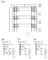
図1(A)は、液晶表示装置の構成例を示す図である。図1(A)に示す液晶表示装置は、画素部10と、走査線駆動回路11と、信号線駆動回路12と、各々が平行又は略平行に配設され、且つ走査線駆動回路11によって電位が制御される、3n本(nは、2以上の自然数)の走査線131、3n本の走査線132、及び3n本の走査線133と、各々が平行又は略平行に配設され、且つ信号線駆動回路12によって電位が制御される、m本(mは、2以上の自然数)の信号線141、m本の信号線142、及びm本の信号線143と、を有する。
図2は、図1(A)に示す液晶表示装置が有する走査線駆動回路11の構成例を示す図である。図2に示す走査線駆動回路11は、3n個の出力端子を有する3つのシフトレジスタ111〜113を有する。なお、シフトレジスタ111が有する出力端子のそれぞれは、画素部10に配設された3n本の走査線131のいずれかに電気的に接続され、シフトレジスタ112が有する出力端子のそれぞれは、画素部10に配設された3n本の走査線132のいずれかに電気的に接続され、シフトレジスタ113が有する出力端子のそれぞれは、画素部10に配設された3n本の走査線133のいずれかに電気的に接続される。すなわち、シフトレジスタ111は、走査線131を駆動するシフトレジスタであり、シフトレジスタ112は、走査線132を駆動するシフトレジスタであり、シフトレジスタ113は、走査線133を駆動するシフトレジスタである。具体的には、シフトレジスタ111は、外部から入力される第1の走査線駆動回路用スタート信号(GSP1)をきっかけとして、1行目に配設された走査線131を起点として順次選択信号をシフト(走査線131を走査線駆動回路用クロック信号(GCK)1/2周期毎に順次選択)する機能を有し、シフトレジスタ112は、外部から入力される第2の走査線駆動回路用スタート信号(GSP2)をきっかけとして、1行目に配設された走査線132を起点として順次選択信号をシフトする機能を有し、シフトレジスタ113は、外部から入力される第3の走査線駆動回路用スタート信号(GSP3)をきっかけとして、1行目に配設された走査線133を起点として順次選択信号をシフトする機能を有する。
上述した走査線駆動回路11の動作例について図3を参照して説明する。なお、図3には、走査線駆動回路用クロック信号(GCK)、シフトレジスタ111が有する3n個の出力端子から出力される信号(SR111out)、シフトレジスタ112が有する3n個の出力端子から出力される信号(SR112out)、及びシフトレジスタ113が有する3n個の出力端子から出力される信号(SR113out)を示している。ここで、サンプリング期間とは、全ての行(1行目乃至3n行目)に配設された全ての画素に対して何らかの画像信号が入力されるのに要する期間である。
図4(A)は、図1(A)に示す液晶表示装置が有する信号線駆動回路12の構成例を示す図である。図4(A)に示す信号線駆動回路12は、m個の出力端子を有するシフトレジスタ120と、m個のトランジスタ121と、m個のトランジスタ122と、m個のトランジスタ123と、を有する。なお、トランジスタ121のゲートは、シフトレジスタ120が有するj番目(jは、1以上m以下の自然数)の出力端子に電気的に接続され、ソース及びドレインの一方が第1の画像信号(DATA1)を供給する配線に電気的に接続され、ソース及びドレインの他方が画素部10においてj列目に配設された信号線141に電気的に接続される。また、トランジスタ122のゲートは、シフトレジスタ120が有するj番目の出力端子に電気的に接続され、ソース及びドレインの一方が第2の画像信号(DATA2)を供給する配線に電気的に接続され、ソース及びドレインの他方が画素部10においてj列目に配設された信号線142に電気的に接続される。また、トランジスタ123のゲートは、シフトレジスタ120が有するj番目の出力端子に電気的に接続され、ソース及びドレインの一方が第3の画像信号(DATA3)を供給する配線に電気的に接続され、ソース及びドレインの他方が画素部10においてj列目に配設された信号線143に電気的に接続される。
図4(B)は、図1(A)に示す液晶表示装置の画素部10の後方に設けられるバックライトの構成例を示す図である。図4(B)に示すバックライトは、赤(R)、緑(G)、青(B)の3色を呈する光源を備えたバックライトユニット16を複数有する。なお、複数のバックライトユニット16は、マトリクス状に配設されており、且つ特定の領域毎に点灯を制御することが可能である。ここでは、3n行m列に配設された複数の画素15に対するバックライトとして、少なくともk行m列毎(ここでは、kは、n/4とする)にバックライトユニット群が設けられ、それらのバックライトユニット群の点滅を独立に制御できることとする。すなわち、当該バックライトが、少なくとも1行目乃至k行目用バックライトユニット群〜(3n−k+1)行目乃至3n行目用バックライトユニット群を有し、それぞれのバックライトユニット群の点滅を独立に制御できることとする。
図5は、上述した液晶表示装置において、バックライトが有する1行目乃至k行目用バックライトユニット群〜(3n−k+1)行目乃至3n行目用バックライトユニット群において点灯される光のタイミング、及び画素部10において1行目に配設されたm個の画素乃至3n行目に配設されたm個の画素に対する画像信号の供給が行われるタイミングを示す図である。具体的には、図5において、1乃至3nは、行数を表し、実線は、該当する行において画像信号が入力されるタイミングを表している。当該液晶表示装置は、サンプリング期間(t1)において、1行目に配設されたm個の画素15からn行目に配設されたm個の画素15を順次選択し、且つ(n+1)行目に配設されたm個の画素15から2n行目に配設されたm個の画素15を順次選択し、且つ(2n+1)行目に配設されたm個の画素15から3n行目に配設されたm個の画素15を順次選択することで、各画素に画像信号を入力することが可能である。具体的に述べると、当該液晶表示装置は、サンプリング期間(t1)において、走査線131を介して1行目に配設されたm個の画素15が有するトランジスタ151からn行目に配設されたm個の画素15が有するトランジスタ151を順次オン状態とすることで、信号線141を介して赤(R)の画像信号を各画素に順次入力することが可能であり、走査線132を介して(n+1)行目に配設されたm個の画素15が有するトランジスタ152から2n行目に配設されたm個の画素15が有するトランジスタ152を順次オン状態とすることで、信号線142を介して青(B)の画像信号を各画素に順次入力することが可能であり、走査線133を介して(2n+1)行目に配設されたm個の画素15が有するトランジスタ153から3n行目に配設されたm個の画素15が有するトランジスタ153を順次オン状態とすることで、信号線143を介して緑(G)の画像信号を各画素に順次入力することが可能である。
本明細書で開示される液晶表示装置は、マトリクス状に配設された画素のうち、複数行に配設された画素に対して同時に画像信号を供給することが可能である。これにより、当該液晶表示装置が有するトランジスタなどの応答速度を変化させることなく、各画素に対する画像信号の入力頻度を増加させることが可能になる。具体的に述べると、上述した液晶表示装置では、走査線駆動回路のクロック周波数などを変化させることなく、各画素に対する画像信号の入力頻度を3倍にすることが可能である。すなわち、当該液晶表示装置は、フィールドシーケンシャル方式によって表示を行う液晶表示装置、又は倍速駆動を行う液晶表示装置として好適である。
上述した構成を有する液晶表示装置は、本発明の一態様であり、当該液晶表示装置と異なる点を有する液晶表示装置も本発明には含まれる。
本実施の形態では、実施の形態1とは異なる構成を有する、フィールドシーケンシャル方式によって表示を行う液晶表示装置の一例について図6〜図8を参照して説明する。
図6(A)は、液晶表示装置の構成例を示す図である。図6(A)に示す液晶表示装置は、画素部30と、走査線駆動回路31と、信号線駆動回路32と、各々が平行又は略平行に配設され、且つ走査線駆動回路31によって電位が制御される3n本(nは、2以上の自然数)の走査線33と、各々が平行又は略平行に配設され、且つ信号線駆動回路32によって電位が制御される、m本(mは、2以上の自然数)の信号線341、m本の信号線342、及びm本の信号線343と、を有する。
図7(A)は、図6(A)に示す液晶表示装置が有する走査線駆動回路31の構成例を示す図である。図7(A)に示す走査線駆動回路31は、n個の出力端子を有するシフトレジスタ311〜313を有する。なお、シフトレジスタ311が有する出力端子のそれぞれは、領域301に配設されたn本の走査線33のいずれかに電気的に接続され、シフトレジスタ312が有する出力端子のそれぞれは、領域302に配設されたn本の走査線33のいずれかに電気的に接続され、シフトレジスタ313が有する出力端子のそれぞれは、領域303に配設されたn本の走査線33のいずれかに電気的に接続される。すなわち、シフトレジスタ311は、領域301において選択信号を供給するシフトレジスタであり、シフトレジスタ312は、領域302において選択信号を供給するシフトレジスタであり、シフトレジスタ313は、領域303において選択信号を供給するシフトレジスタである。具体的には、シフトレジスタ311は、外部から入力される走査線駆動回路用スタート信号(GSP)をきっかけとして、1行目に配設された走査線33を起点として順次選択信号をシフト(走査線33を走査線駆動回路用クロック信号(GCK)1/2周期毎に順次選択)する機能を有し、シフトレジスタ312は、外部から入力される走査線駆動回路用スタート信号(GSP)をきっかけとして、(n+1)行目に配設された走査線33を起点として順次選択信号をシフトする機能を有し、シフトレジスタ313は、外部から入力される走査線駆動回路用スタート信号(GSP)をきっかけとして、(2n+1)行目に配設された走査線33を起点として順次選択信号をシフトする機能を有する。
上述した走査線駆動回路31の動作例について図7(B)を参照して説明する。なお、図7(B)には、走査線駆動回路用クロック信号(GCK)、シフトレジスタ311が有するn個の出力端子から出力される信号(SR311out)、シフトレジスタ312が有するn個の出力端子から出力される信号(SR312out)、及びシフトレジスタ313が有するn個の出力端子から出力される信号(SR313out)を示している。
図8は、図6(A)に示す液晶表示装置が有する信号線駆動回路32の構成例を示す図である。図8に示す信号線駆動回路32は、m個の出力端子を有するシフトレジスタ320と、m個のトランジスタ321と、m個のトランジスタ322と、m個のトランジスタ323と、を有する。なお、トランジスタ321のゲートは、シフトレジスタ320が有するj番目(jは、1以上m以下の自然数)の出力端子に電気的に接続され、ソース及びドレインの一方が第1の画像信号(data1)を供給する配線に電気的に接続され、ソース及びドレインの他方が画素部30においてj列目に配設された信号線341に電気的に接続される。また、トランジスタ322のゲートは、シフトレジスタ320が有するj番目の出力端子に電気的に接続され、ソース及びドレインの一方が第2の画像信号(data2)を供給する配線に電気的に接続され、ソース及びドレインの他方が画素部30においてj列目に配設された信号線342に電気的に接続される。また、トランジスタ323のゲートは、シフトレジスタ320が有するj番目の出力端子に電気的に接続され、ソース及びドレインの一方が第3の画像信号(data3)を供給する配線に電気的に接続され、ソース及びドレインの他方が画素部30においてj列目に配設された信号線343に電気的に接続される。
本実施の形態の液晶表示装置のバックライトとして、実施の形態1に示したバックライトを適用することが可能である。そのため、ここでは前述の説明を援用することとする。
本実施の形態の液晶表示装置は、実施の形態1に示した液晶表示装置と同様の動作(図5参照)を行うことが可能である。すなわち、本実施の形態の液晶表示装置は、サンプリング期間(T1)において、1行目に配設されたm個の画素351からn行目に配設されたm個の画素351を順次選択し、且つ(n+1)行目に配設されたm個の画素352から2n行目に配設されたm個の画素352を順次選択し、且つ(2n+1)行目に配設されたm個の画素353から3n行目に配設されたm個の画素353を順次選択することで、各画素に画像信号を入力することが可能である。
本実施の形態の液晶表示装置は、実施の形態1に示した液晶表示装置と同様の作用を有する液晶表示装置である。さらに、本実施の形態の液晶表示装置は、実施の形態1に示した液晶表示装置と比較して、画素部に配設される走査線の本数及び各画素に設けられるトランジスタの数を低減することができ、開口率をさらに向上させることが可能である。また、画素部に配設される走査線の本数が低減されることで信号線と走査線とが重畳することによって生じる寄生容量を低減することができるため、信号線を高速駆動することが可能である。また、走査線駆動回路の回路面積を縮小すること、及び走査線駆動回路の動作に必要とされる信号を低減すること(複数のシフトレジスタに別々の走査線駆動回路用スタート信号を入力する必要がない)が可能である。
本実施の形態の液晶表示装置は、本発明の一態様であり、当該液晶表示装置と異なる点を有する液晶表示装置も本発明には含まれる。例えば、本実施の形態の液晶表示装置の構成を、実施の形態1の変形例に示した構成に変更することが可能である。具体的には、本実施の形態の液晶表示装置が有するシフトレジスタを同等の機能を有する回路(デコーダなど)に置換することなどが可能である。
本実施の形態では、実施の形態1又は2に示した液晶表示装置の具体的な構成について、説明する。
図9に、本発明の一態様に係る液晶表示装置の、画素の断面図を一例として示す。図9に示すトランジスタ1401は、多結晶半導体又は単結晶半導体を用いた半導体層1402と、半導体層1402上のゲート絶縁層1403と、ゲート絶縁層1403を間に挟んで半導体層1402と重なるゲート層1404とを少なくとも有する。半導体層1402には、ソースまたはドレインとして機能する一対の不純物領域1405が形成されている。
次いで、画素部の形成された基板に、駆動回路が形成された基板を直接実装する場合の、端子間の接続の仕方について説明する。
次いで、画素部と駆動回路の一形態について説明する。なお、ここでは、画素部と駆動回路の一部又は全部を構成するトランジスタとして多結晶半導体をチャネル形成領域に有するトランジスタを用いることとする。この場合、画素部と共に駆動回路の一部または全てを、一の基板に作り込むことができる。
次いで、本発明の一態様に係る液晶表示装置のパネルの外観について、図12を用いて説明する。図12(A)は、基板4001と対向基板4006とをシール材4005によって接着させたパネルの上面図であり、図12(B)は、図12(A)の破線A−A’における断面図に相当する。
本発明の一態様に係る液晶表示装置は、タッチパネルと呼ばれる位置入力装置を有していても良い。図14(A)に、タッチパネル1620と、パネル1621とを重ね合わせている様子を示す。
本発明の一態様に係る液晶表示装置は、フォトセンサを画素部に有していても良い。図16(A)に、フォトセンサを有する画素部の構造の一例を、模式的に示す。
次に、チャネル形成領域が多結晶半導体を含むトランジスタの作製方法の一例について述べる。
次に、チャネル形成領域が単結晶半導体を含むトランジスタの作製方法の一例について述べる。なお、ここでは、SOI基板を用いて作製されるトランジスタの一例について述べる。
以下では、本明細書で開示される液晶表示装置を搭載した電子機器の例について図18を参照して説明する。
11 走査線駆動回路
12 信号線駆動回路
15 画素
16 バックライトユニット
30 画素部
31 走査線駆動回路
32 信号線駆動回路
33 走査線
111 シフトレジスタ
112 シフトレジスタ
113 シフトレジスタ
120 シフトレジスタ
121 トランジスタ
122 トランジスタ
123 トランジスタ
131 走査線
132 走査線
133 走査線
141 信号線
142 信号線
143 信号線
151 トランジスタ
152 トランジスタ
153 トランジスタ
154 容量素子
155 液晶素子
301 領域
302 領域
303 領域
311 シフトレジスタ
312 シフトレジスタ
313 シフトレジスタ
320 シフトレジスタ
321 トランジスタ
322 トランジスタ
323 トランジスタ
341 信号線
342 信号線
343 信号線
351 画素
352 画素
353 画素
500 基板
501 絶縁層
502 半導体層
503 半導体層
504 半導体層
505 トランジスタ
506 トランジスタ
507 ゲート絶縁層
508 導電膜
509 導電膜
510 ゲート層
511 ゲート層
512 絶縁膜
513 絶縁膜
514 導電膜
515 導電膜
516 導電膜
517 導電膜
600 ボンド基板
601 絶縁層
602 脆化層
603 ベース基板
604 半導体層
610 半導体層
611 半導体層
612 半導体層
613 ゲート絶縁層
614 ゲート層
615 不純物領域
616 不純物領域
617 サイドウォール
618 高濃度不純物領域
619 低濃度不純物領域
620 チャネル形成領域
621 高濃度不純物領域
622 低濃度不純物領域
623 チャネル形成領域
624 トランジスタ
625 トランジスタ
626 絶縁膜
627 絶縁膜
628 導電膜
629 導電膜
900 基板
901 基板
903 接着剤
904 端子
905 ワイヤ
906 トランジスタ
907 パッド
910 基板
911 基板
912 パッド
913 ソルダーボール
914 トランジスタ
916 端子
920 基板
921 基板
922 パッド
924 トランジスタ
926 端子
927 導電性樹脂
1401 トランジスタ
1402 半導体層
1403 ゲート絶縁層
1404 ゲート層
1405 不純物領域
1406 導電膜
1407 導電膜
1408 絶縁層
1409 画素電極
1411 配向膜
1413 対向電極
1414 配向膜
1415 液晶
1416 シール材
1417 スペーサ
1420 対向基板
1601 パネル
1602 拡散板
1603 プリズムシート
1604 拡散板
1605 導光板
1607 バックライトパネル
1608 回路基板
1609 COFテープ
1610 FPC
1611 基板
1612 バックライト
1620 タッチパネル
1621 パネル
1622 位置検出部
1623 画素部
1630 第1電極
1631 第2電極
1640 第1電極
1641 第2電極
1642 導電膜
1643 導電膜
1644 絶縁層
1650 画素部
1651 画素
1652 フォトセンサ
1653 フォトダイオード
1654 トランジスタ
1655 トランジスタ
1656 リセット信号線
1657 基準信号線
1658 ゲート信号線
1659 出力信号線
2201 本体
2202 筐体
2203 表示部
2204 キーボード
2211 本体
2212 スタイラス
2213 表示部
2214 操作ボタン
2215 外部インターフェイス
2220 電子書籍
2221 筐体
2223 筐体
2225 表示部
2227 表示部
2231 電源ボタン
2233 操作キー
2235 スピーカー
2237 軸部
2240 筐体
2241 筐体
2242 表示パネル
2243 スピーカー
2244 マイクロフォン
2245 操作キー
2246 ポインティングデバイス
2247 カメラ用レンズ
2248 外部接続端子
2249 太陽電池セル
2250 外部メモリスロット
2261 本体
2263 接眼部
2264 操作スイッチ
2265 表示部
2266 バッテリー
2267 表示部
2270 テレビジョン装置
2271 筐体
2273 表示部
2275 スタンド
2277 表示部
2279 操作キー
2280 リモコン操作機
3511 トランジスタ
3512 容量素子
3514 液晶素子
3521 トランジスタ
3531 トランジスタ
4001 基板
4002 画素部
4003 信号線駆動回路
4004 走査線駆動回路
4005 シール材
4006 対向基板
4007 液晶
4009 トランジスタ
4010 トランジスタ
4011 液晶素子
4014 引き回し配線
4015 引き回し配線
4016 接続端子
4018 FPC
4019 異方性導電膜
4021 基板
4022 トランジスタ
4030 画素電極
4031 対向電極
4035 スペーサ
5001 基板
5002 画素部
5003 信号線駆動回路
5004 走査線駆動回路
5005 シール材
5006 対向基板
5007 液晶
5009 トランジスタ
5010 トランジスタ
5011 液晶素子
5014 引き回し配線
5015 引き回し配線
5016 接続端子
5018 FPC
5019 異方性導電膜
5021 基板
5022 トランジスタ
5030 画素電極
5031 対向電極
5035 スペーサ
6001 基板
6002 画素部
6003 走査線駆動回路
6004 基板
6005 FPC
6006 対向基板
6101 基板
6102 画素部
6103 走査線駆動回路
6104 基板
6105 FPC
6106 対向基板
6201 基板
6202 画素部
6203 走査線駆動回路
6204 基板
6205 FPC
6206 対向基板
6207 信号線駆動回路の一部
6301 基板
6302 画素部
6303 走査線駆動回路
6304 信号線駆動回路
6305 FPC
6306 対向基板
Claims (1)
- 複数の画素を有し、
前記画素は、第1のトランジスタと、第2のトランジスタと、第3のトランジスタと、液晶素子と、を有し、
前記第1のトランジスタのチャネル形成領域は、多結晶半導体または単結晶半導体を含み、
前記第2のトランジスタのチャネル形成領域は、多結晶半導体または単結晶半導体を含み、
前記第3のトランジスタのチャネル形成領域は、多結晶半導体または単結晶半導体を含む液晶表示装置の駆動方法であって、
第1の走査線から第nの走査線(nは、3以上の自然数)に対して順次選択信号を入力することで、第1行目の画素乃至第n行目の画素に対応する前記第1のトランジスタをオン状態とし、前記第1のトランジスタを介して前記液晶素子に画像信号を入力し、
且つ、
第(n+1)の走査線から第2nの走査線に対して順次選択信号を入力することで、第(n+1)行目の画素乃至第2n行目の画素に対応する前記第2のトランジスタをオン状態とし、前記第2のトランジスタを介して前記液晶素子に画像信号を入力し、
且つ、
第(2n+1)の走査線から第3nの走査線に対して順次選択信号を入力することで、第(2n+1)行目の画素乃至第3n行目の画素に対応する前記第3のトランジスタをオン状態とし、前記第3のトランジスタを介して前記液晶素子に画像信号を入力する期間において、
第kの走査線(kは、2以上n未満の自然数)と、第(n+k)の走査線と、第(2n+k)の走査線に対する選択信号の入力が終了した後に、第1行目の画素乃至第k行目の画素に対応する光源と、第(n+1)行目の画素乃至第(n+k)行目の画素に対応する光源と、第(2n+1)行目の画素乃至第(2n+k)行目の画素に対応する光源とを発光させ、
前記期間において、第1行目の画素乃至第k行目の画素に対応する光源が呈する光の色と、第(n+1)行目の画素乃至第(n+k)行目の画素に対応する光源が呈する光の色と、第(2n+1)行目の画素乃至第(2n+k)行目の画素に対応する光源が呈する光の色とが異なり、
第1行目の画素乃至第k行目の画素に対応する光源が呈する光の色は、赤、緑、及び青のうちの第1の色であり、
第(n+1)行目の画素乃至第(n+k)行目の画素に対応する光源が呈する光の色は、赤、緑、及び青のうちの前記第1の色と異なる第2の色であり、
第(2n+1)行目の画素乃至第(2n+k)行目の画素に対応する光源が呈する光の色は、赤、緑、及び青のうちの前記第1の色と異なり且つ前記第2の色と異なる第3の色であることを特徴とする液晶表示装置の駆動方法。
Priority Applications (1)
| Application Number | Priority Date | Filing Date | Title |
|---|---|---|---|
| JP2011083270A JP5774893B2 (ja) | 2010-04-09 | 2011-04-05 | 液晶表示装置の駆動方法 |
Applications Claiming Priority (9)
| Application Number | Priority Date | Filing Date | Title |
|---|---|---|---|
| JP2010090938 | 2010-04-09 | ||
| JP2010090944 | 2010-04-09 | ||
| JP2010090938 | 2010-04-09 | ||
| JP2010090944 | 2010-04-09 | ||
| JP2010114445 | 2010-05-18 | ||
| JP2010114440 | 2010-05-18 | ||
| JP2010114440 | 2010-05-18 | ||
| JP2010114445 | 2010-05-18 | ||
| JP2011083270A JP5774893B2 (ja) | 2010-04-09 | 2011-04-05 | 液晶表示装置の駆動方法 |
Publications (3)
| Publication Number | Publication Date |
|---|---|
| JP2012003237A JP2012003237A (ja) | 2012-01-05 |
| JP2012003237A5 JP2012003237A5 (ja) | 2014-03-06 |
| JP5774893B2 true JP5774893B2 (ja) | 2015-09-09 |
Family
ID=44760590
Family Applications (1)
| Application Number | Title | Priority Date | Filing Date |
|---|---|---|---|
| JP2011083270A Expired - Fee Related JP5774893B2 (ja) | 2010-04-09 | 2011-04-05 | 液晶表示装置の駆動方法 |
Country Status (3)
| Country | Link |
|---|---|
| US (1) | US8907881B2 (ja) |
| JP (1) | JP5774893B2 (ja) |
| KR (1) | KR20110113581A (ja) |
Families Citing this family (25)
| Publication number | Priority date | Publication date | Assignee | Title |
|---|---|---|---|---|
| US8830278B2 (en) | 2010-04-09 | 2014-09-09 | Semiconductor Energy Laboratory Co., Ltd. | Liquid crystal display device and method for driving the same |
| KR101748901B1 (ko) | 2010-04-09 | 2017-06-19 | 가부시키가이샤 한도오따이 에네루기 켄큐쇼 | 액정 표시 장치 및 그 구동 방법 |
| CN103038813B (zh) | 2010-05-25 | 2016-07-27 | 株式会社半导体能源研究所 | 液晶显示装置及其驱动方法 |
| US9286848B2 (en) * | 2010-07-01 | 2016-03-15 | Semiconductor Energy Laboratory Co., Ltd. | Method for driving liquid crystal display device |
| KR20130090405A (ko) | 2010-07-02 | 2013-08-13 | 가부시키가이샤 한도오따이 에네루기 켄큐쇼 | 액정 표시 장치 |
| US8988337B2 (en) | 2010-07-02 | 2015-03-24 | Semiconductor Energy Laboratory Co., Ltd. | Driving method of liquid crystal display device |
| CN102971784B (zh) | 2010-07-02 | 2016-08-03 | 株式会社半导体能源研究所 | 液晶显示装置及驱动液晶显示装置的方法 |
| JP2012048220A (ja) | 2010-07-26 | 2012-03-08 | Semiconductor Energy Lab Co Ltd | 液晶表示装置及びその駆動方法 |
| TWI562109B (en) | 2010-08-05 | 2016-12-11 | Semiconductor Energy Lab Co Ltd | Driving method of liquid crystal display device |
| JP5825895B2 (ja) | 2010-08-06 | 2015-12-02 | 株式会社半導体エネルギー研究所 | 液晶表示装置 |
| JP2012103683A (ja) | 2010-10-14 | 2012-05-31 | Semiconductor Energy Lab Co Ltd | 表示装置及び表示装置の駆動方法 |
| JP2012242452A (ja) * | 2011-05-16 | 2012-12-10 | Japan Display East Co Ltd | 表示装置 |
| JP5717880B2 (ja) * | 2011-12-28 | 2015-05-13 | シャープ株式会社 | タッチパネルおよびタッチパネル付き表示装置 |
| JP2014032399A (ja) | 2012-07-13 | 2014-02-20 | Semiconductor Energy Lab Co Ltd | 液晶表示装置 |
| WO2016002424A1 (ja) * | 2014-07-04 | 2016-01-07 | シャープ株式会社 | 液晶表示装置 |
| JP2016057616A (ja) * | 2014-09-05 | 2016-04-21 | 株式会社半導体エネルギー研究所 | 表示パネル、入出力装置、情報処理装置 |
| KR102316212B1 (ko) * | 2015-04-30 | 2021-10-22 | 삼성디스플레이 주식회사 | 터치 센서 및 이의 제조 방법 |
| KR102535271B1 (ko) * | 2016-01-18 | 2023-05-23 | 삼성디스플레이 주식회사 | 터치 패널 및 이를 구비한 표시 장치 |
| US10096292B2 (en) * | 2016-02-26 | 2018-10-09 | a.u. Vista Inc. | Liquid crystal display systems and related methods with pixel elements driven at different frequencies |
| CN105788529A (zh) * | 2016-05-10 | 2016-07-20 | 上海天马有机发光显示技术有限公司 | 一种有机发光显示面板及其驱动方法 |
| KR102836512B1 (ko) * | 2017-01-18 | 2025-07-22 | 삼성전자주식회사 | 지문 인식 기능을 가지는 전자 장치 |
| US10586734B2 (en) * | 2017-11-20 | 2020-03-10 | Tokyo Electron Limited | Method of selective film deposition for forming fully self-aligned vias |
| US20190245011A1 (en) | 2018-02-06 | 2019-08-08 | Innolux Corporation | Display device |
| WO2020121110A1 (ja) * | 2018-12-14 | 2020-06-18 | 株式会社半導体エネルギー研究所 | 表示装置、情報処理装置 |
| WO2021130598A1 (ja) * | 2019-12-27 | 2021-07-01 | 株式会社半導体エネルギー研究所 | 記憶装置およびその作製方法 |
Family Cites Families (40)
| Publication number | Priority date | Publication date | Assignee | Title |
|---|---|---|---|---|
| EP0797182A1 (en) * | 1996-03-19 | 1997-09-24 | Hitachi, Ltd. | Active matrix LCD with data holding circuit in each pixel |
| JP3280307B2 (ja) * | 1998-05-11 | 2002-05-13 | インターナショナル・ビジネス・マシーンズ・コーポレーション | 液晶表示装置 |
| EP0997868B1 (en) | 1998-10-30 | 2012-03-14 | Semiconductor Energy Laboratory Co., Ltd. | Field sequential liquid crystal display device and driving method thereof, and head mounted display |
| US6597348B1 (en) | 1998-12-28 | 2003-07-22 | Semiconductor Energy Laboratory Co., Ltd. | Information-processing device |
| US7145536B1 (en) | 1999-03-26 | 2006-12-05 | Semiconductor Energy Laboratory Co., Ltd. | Liquid crystal display device |
| US7339568B2 (en) * | 1999-04-16 | 2008-03-04 | Samsung Electronics Co., Ltd. | Signal transmission film and a liquid crystal display panel having the same |
| JP3556150B2 (ja) * | 1999-06-15 | 2004-08-18 | シャープ株式会社 | 液晶表示方法および液晶表示装置 |
| TW522374B (en) * | 2000-08-08 | 2003-03-01 | Semiconductor Energy Lab | Electro-optical device and driving method of the same |
| US6992652B2 (en) * | 2000-08-08 | 2006-01-31 | Semiconductor Energy Laboratory Co., Ltd. | Liquid crystal display device and driving method thereof |
| US7385579B2 (en) | 2000-09-29 | 2008-06-10 | Semiconductor Energy Laboratory Co., Ltd. | Liquid crystal display device and method of driving the same |
| US6747623B2 (en) * | 2001-02-09 | 2004-06-08 | Semiconductor Energy Laboratory Co., Ltd. | Liquid crystal display device and method of driving the same |
| JP2003255912A (ja) | 2002-03-05 | 2003-09-10 | Seiko Epson Corp | 電気光学装置、それを用いた電子機器および電気光学装置の駆動方法 |
| EP1388842B1 (en) * | 2002-08-09 | 2013-10-02 | Semiconductor Energy Laboratory Co., Ltd. | Multi-window display device and method of driving the same |
| CN100580753C (zh) | 2002-11-29 | 2010-01-13 | 株式会社半导体能源研究所 | 显示装置和电子装置 |
| CN100557667C (zh) | 2004-04-22 | 2009-11-04 | 株式会社半导体能源研究所 | 发光装置及其驱动方法 |
| WO2006059737A1 (en) * | 2004-11-30 | 2006-06-08 | Semiconductor Energy Laboratory Co., Ltd. | Display device and driving method thereof, semiconductor device, and electronic apparatus |
| JP2006220685A (ja) | 2005-02-08 | 2006-08-24 | 21 Aomori Sangyo Sogo Shien Center | スキャンバックライトを用いた分割駆動フィールドシーケンシャルカラー液晶ディスプレイの駆動方法および装置 |
| US7932891B2 (en) * | 2005-09-13 | 2011-04-26 | Chunghwa Picture Tubes, Ltd. | Driving method and system thereof for LCD multiple scan |
| US7728810B2 (en) * | 2005-11-28 | 2010-06-01 | Lg Display Co., Ltd. | Display device and method for driving the same |
| EP1832915B1 (en) | 2006-01-31 | 2012-04-18 | Semiconductor Energy Laboratory Co., Ltd. | Display device with improved contrast |
| JP2007264211A (ja) | 2006-03-28 | 2007-10-11 | 21 Aomori Sangyo Sogo Shien Center | 色順次表示方式液晶表示装置用の色表示方法 |
| US8106865B2 (en) * | 2006-06-02 | 2012-01-31 | Semiconductor Energy Laboratory Co., Ltd. | Display device and driving method thereof |
| US8154493B2 (en) | 2006-06-02 | 2012-04-10 | Semiconductor Energy Laboratory Co., Ltd. | Liquid crystal display device, driving method of the same, and electronic device using the same |
| KR101261607B1 (ko) * | 2006-07-25 | 2013-05-08 | 삼성디스플레이 주식회사 | 액정 표시 장치 |
| JP5177999B2 (ja) | 2006-12-05 | 2013-04-10 | 株式会社半導体エネルギー研究所 | 液晶表示装置 |
| US8514165B2 (en) * | 2006-12-28 | 2013-08-20 | Semiconductor Energy Laboratory Co., Ltd. | Semiconductor device |
| JP5200209B2 (ja) | 2007-08-08 | 2013-06-05 | エプソンイメージングデバイス株式会社 | 液晶表示装置 |
| JP5075533B2 (ja) | 2007-08-29 | 2012-11-21 | エプソンイメージングデバイス株式会社 | 液晶表示装置 |
| KR101303533B1 (ko) * | 2008-04-29 | 2013-09-03 | 엘지디스플레이 주식회사 | 액정표시장치와 그 구동방법 |
| KR101301422B1 (ko) * | 2008-04-30 | 2013-08-28 | 엘지디스플레이 주식회사 | 액정표시장치와 그 구동방법 |
| KR101303494B1 (ko) * | 2008-04-30 | 2013-09-03 | 엘지디스플레이 주식회사 | 액정표시장치와 그 구동방법 |
| JP5384088B2 (ja) * | 2008-11-28 | 2014-01-08 | 株式会社ジャパンディスプレイ | 表示装置 |
| KR101310379B1 (ko) * | 2008-12-03 | 2013-09-23 | 엘지디스플레이 주식회사 | 액정표시장치와 그 구동방법 |
| JP5202395B2 (ja) * | 2009-03-09 | 2013-06-05 | 株式会社半導体エネルギー研究所 | タッチパネル、電子機器 |
| TWI496042B (zh) | 2009-07-02 | 2015-08-11 | Semiconductor Energy Lab | 觸控面板及其驅動方法 |
| JP2011083269A (ja) * | 2009-10-17 | 2011-04-28 | Yoshiyuki Goto | 釣り用スナップ |
| US8830278B2 (en) | 2010-04-09 | 2014-09-09 | Semiconductor Energy Laboratory Co., Ltd. | Liquid crystal display device and method for driving the same |
| KR101748901B1 (ko) | 2010-04-09 | 2017-06-19 | 가부시키가이샤 한도오따이 에네루기 켄큐쇼 | 액정 표시 장치 및 그 구동 방법 |
| US8988337B2 (en) | 2010-07-02 | 2015-03-24 | Semiconductor Energy Laboratory Co., Ltd. | Driving method of liquid crystal display device |
| JP2012048220A (ja) | 2010-07-26 | 2012-03-08 | Semiconductor Energy Lab Co Ltd | 液晶表示装置及びその駆動方法 |
-
2011
- 2011-04-01 US US13/078,209 patent/US8907881B2/en not_active Expired - Fee Related
- 2011-04-05 JP JP2011083270A patent/JP5774893B2/ja not_active Expired - Fee Related
- 2011-04-07 KR KR1020110032339A patent/KR20110113581A/ko not_active Ceased
Also Published As
| Publication number | Publication date |
|---|---|
| US20110248970A1 (en) | 2011-10-13 |
| US8907881B2 (en) | 2014-12-09 |
| JP2012003237A (ja) | 2012-01-05 |
| KR20110113581A (ko) | 2011-10-17 |
Similar Documents
| Publication | Publication Date | Title |
|---|---|---|
| JP5774893B2 (ja) | 液晶表示装置の駆動方法 | |
| JP7809227B2 (ja) | 表示装置 | |
| KR101457656B1 (ko) | 반도체장치의 제조방법, 표시장치의 제조방법, 반도체장치,표시장치 및 전자기기 | |
| US8633590B2 (en) | Semiconductor device and method for manufacturing the same | |
| JP5647931B2 (ja) | 液晶表示装置の駆動方法 | |
| TWI453863B (zh) | 絕緣體上矽基板之製造方法 | |
| JP5716074B2 (ja) | 半導体装置の作製方法 | |
| TWI464510B (zh) | 液晶顯示裝置 | |
| CN101393859B (zh) | 设置有半导体膜的衬底及其制造方法 | |
| TW200910454A (en) | Method for manufacturing semiconductor device | |
| KR20010110360A (ko) | 반도체 장치 제조방법 | |
| TW201030857A (en) | Method for manufacturing semiconductor device | |
| CN101308853A (zh) | 半导体装置 | |
| JP5142546B2 (ja) | 半導体装置及びその作製方法 | |
| JP2001156295A (ja) | 半導体装置の作製方法 |
Legal Events
| Date | Code | Title | Description |
|---|---|---|---|
| A521 | Request for written amendment filed |
Free format text: JAPANESE INTERMEDIATE CODE: A523 Effective date: 20140122 |
|
| A621 | Written request for application examination |
Free format text: JAPANESE INTERMEDIATE CODE: A621 Effective date: 20140122 |
|
| A977 | Report on retrieval |
Free format text: JAPANESE INTERMEDIATE CODE: A971007 Effective date: 20141006 |
|
| A131 | Notification of reasons for refusal |
Free format text: JAPANESE INTERMEDIATE CODE: A131 Effective date: 20141014 |
|
| A131 | Notification of reasons for refusal |
Free format text: JAPANESE INTERMEDIATE CODE: A132 Effective date: 20150317 |
|
| A521 | Request for written amendment filed |
Free format text: JAPANESE INTERMEDIATE CODE: A523 Effective date: 20150325 |
|
| TRDD | Decision of grant or rejection written | ||
| A01 | Written decision to grant a patent or to grant a registration (utility model) |
Free format text: JAPANESE INTERMEDIATE CODE: A01 Effective date: 20150630 |
|
| A61 | First payment of annual fees (during grant procedure) |
Free format text: JAPANESE INTERMEDIATE CODE: A61 Effective date: 20150702 |
|
| R150 | Certificate of patent or registration of utility model |
Ref document number: 5774893 Country of ref document: JP Free format text: JAPANESE INTERMEDIATE CODE: R150 |
|
| R250 | Receipt of annual fees |
Free format text: JAPANESE INTERMEDIATE CODE: R250 |
|
| R250 | Receipt of annual fees |
Free format text: JAPANESE INTERMEDIATE CODE: R250 |
|
| R250 | Receipt of annual fees |
Free format text: JAPANESE INTERMEDIATE CODE: R250 |
|
| R250 | Receipt of annual fees |
Free format text: JAPANESE INTERMEDIATE CODE: R250 |
|
| R250 | Receipt of annual fees |
Free format text: JAPANESE INTERMEDIATE CODE: R250 |
|
| LAPS | Cancellation because of no payment of annual fees |