JP5787247B2 - サーマルヘッドの製造方法 - Google Patents
サーマルヘッドの製造方法 Download PDFInfo
- Publication number
- JP5787247B2 JP5787247B2 JP2010213291A JP2010213291A JP5787247B2 JP 5787247 B2 JP5787247 B2 JP 5787247B2 JP 2010213291 A JP2010213291 A JP 2010213291A JP 2010213291 A JP2010213291 A JP 2010213291A JP 5787247 B2 JP5787247 B2 JP 5787247B2
- Authority
- JP
- Japan
- Prior art keywords
- substrate
- groove
- depth
- width
- thermal head
- Prior art date
- Legal status (The legal status is an assumption and is not a legal conclusion. Google has not performed a legal analysis and makes no representation as to the accuracy of the status listed.)
- Expired - Fee Related
Links
- 238000004519 manufacturing process Methods 0.000 title claims description 27
- 239000000758 substrate Substances 0.000 claims description 178
- 238000010438 heat treatment Methods 0.000 claims description 38
- 238000000034 method Methods 0.000 claims description 30
- 238000005259 measurement Methods 0.000 claims description 21
- 238000013461 design Methods 0.000 claims description 19
- 230000020169 heat generation Effects 0.000 description 21
- 238000005530 etching Methods 0.000 description 15
- 238000012545 processing Methods 0.000 description 13
- 239000010408 film Substances 0.000 description 11
- 238000011156 evaluation Methods 0.000 description 10
- 238000005304 joining Methods 0.000 description 10
- 239000000463 material Substances 0.000 description 9
- 230000001681 protective effect Effects 0.000 description 9
- 239000010410 layer Substances 0.000 description 5
- KRHYYFGTRYWZRS-UHFFFAOYSA-N Fluorane Chemical compound F KRHYYFGTRYWZRS-UHFFFAOYSA-N 0.000 description 4
- 206010037660 Pyrexia Diseases 0.000 description 4
- 230000015572 biosynthetic process Effects 0.000 description 4
- 229920002120 photoresistant polymer Polymers 0.000 description 4
- 238000005498 polishing Methods 0.000 description 4
- 239000000243 solution Substances 0.000 description 4
- 238000001039 wet etching Methods 0.000 description 4
- 238000005229 chemical vapour deposition Methods 0.000 description 3
- 238000005520 cutting process Methods 0.000 description 3
- 238000001312 dry etching Methods 0.000 description 3
- 239000007772 electrode material Substances 0.000 description 3
- 239000011521 glass Substances 0.000 description 3
- 238000001020 plasma etching Methods 0.000 description 3
- 238000004544 sputter deposition Methods 0.000 description 3
- 239000010409 thin film Substances 0.000 description 3
- 239000012790 adhesive layer Substances 0.000 description 2
- 238000006073 displacement reaction Methods 0.000 description 2
- 230000004927 fusion Effects 0.000 description 2
- 238000005488 sandblasting Methods 0.000 description 2
- WGTYBPLFGIVFAS-UHFFFAOYSA-M tetramethylammonium hydroxide Chemical compound [OH-].C[N+](C)(C)C WGTYBPLFGIVFAS-UHFFFAOYSA-M 0.000 description 2
- 238000007740 vapor deposition Methods 0.000 description 2
- 229910018125 Al-Si Inorganic materials 0.000 description 1
- 229910018520 Al—Si Inorganic materials 0.000 description 1
- OKTJSMMVPCPJKN-UHFFFAOYSA-N Carbon Chemical compound [C] OKTJSMMVPCPJKN-UHFFFAOYSA-N 0.000 description 1
- GRYLNZFGIOXLOG-UHFFFAOYSA-N Nitric acid Chemical compound O[N+]([O-])=O GRYLNZFGIOXLOG-UHFFFAOYSA-N 0.000 description 1
- 229910003564 SiAlON Inorganic materials 0.000 description 1
- 229910004298 SiO 2 Inorganic materials 0.000 description 1
- -1 Ta 2 O 5 Inorganic materials 0.000 description 1
- 229910052782 aluminium Inorganic materials 0.000 description 1
- 229910052799 carbon Inorganic materials 0.000 description 1
- 238000004140 cleaning Methods 0.000 description 1
- 229910052802 copper Inorganic materials 0.000 description 1
- 230000007797 corrosion Effects 0.000 description 1
- 238000005260 corrosion Methods 0.000 description 1
- 230000007547 defect Effects 0.000 description 1
- 238000010586 diagram Methods 0.000 description 1
- 238000005553 drilling Methods 0.000 description 1
- 230000000694 effects Effects 0.000 description 1
- 229910052737 gold Inorganic materials 0.000 description 1
- 238000005338 heat storage Methods 0.000 description 1
- 238000009413 insulation Methods 0.000 description 1
- 238000007733 ion plating Methods 0.000 description 1
- 239000011259 mixed solution Substances 0.000 description 1
- 229910021421 monocrystalline silicon Inorganic materials 0.000 description 1
- 229910017604 nitric acid Inorganic materials 0.000 description 1
- 238000000059 patterning Methods 0.000 description 1
- 229910052697 platinum Inorganic materials 0.000 description 1
- 239000004065 semiconductor Substances 0.000 description 1
- 229910021332 silicide Inorganic materials 0.000 description 1
- FVBUAEGBCNSCDD-UHFFFAOYSA-N silicide(4-) Chemical compound [Si-4] FVBUAEGBCNSCDD-UHFFFAOYSA-N 0.000 description 1
- 229910052709 silver Inorganic materials 0.000 description 1
- 239000000126 substance Substances 0.000 description 1
- 230000003746 surface roughness Effects 0.000 description 1
- 238000012546 transfer Methods 0.000 description 1
Images





Classifications
-
- H—ELECTRICITY
- H01—ELECTRIC ELEMENTS
- H01C—RESISTORS
- H01C17/00—Apparatus or processes specially adapted for manufacturing resistors
- H01C17/06—Apparatus or processes specially adapted for manufacturing resistors adapted for coating resistive material on a base
- H01C17/065—Apparatus or processes specially adapted for manufacturing resistors adapted for coating resistive material on a base by thick film techniques, e.g. serigraphy
-
- B—PERFORMING OPERATIONS; TRANSPORTING
- B41—PRINTING; LINING MACHINES; TYPEWRITERS; STAMPS
- B41J—TYPEWRITERS; SELECTIVE PRINTING MECHANISMS, i.e. MECHANISMS PRINTING OTHERWISE THAN FROM A FORME; CORRECTION OF TYPOGRAPHICAL ERRORS
- B41J2/00—Typewriters or selective printing mechanisms characterised by the printing or marking process for which they are designed
- B41J2/315—Typewriters or selective printing mechanisms characterised by the printing or marking process for which they are designed characterised by selective application of heat to a heat sensitive printing or impression-transfer material
- B41J2/32—Typewriters or selective printing mechanisms characterised by the printing or marking process for which they are designed characterised by selective application of heat to a heat sensitive printing or impression-transfer material using thermal heads
- B41J2/335—Structure of thermal heads
-
- B—PERFORMING OPERATIONS; TRANSPORTING
- B41—PRINTING; LINING MACHINES; TYPEWRITERS; STAMPS
- B41J—TYPEWRITERS; SELECTIVE PRINTING MECHANISMS, i.e. MECHANISMS PRINTING OTHERWISE THAN FROM A FORME; CORRECTION OF TYPOGRAPHICAL ERRORS
- B41J2/00—Typewriters or selective printing mechanisms characterised by the printing or marking process for which they are designed
- B41J2/315—Typewriters or selective printing mechanisms characterised by the printing or marking process for which they are designed characterised by selective application of heat to a heat sensitive printing or impression-transfer material
- B41J2/32—Typewriters or selective printing mechanisms characterised by the printing or marking process for which they are designed characterised by selective application of heat to a heat sensitive printing or impression-transfer material using thermal heads
- B41J2/335—Structure of thermal heads
- B41J2/33585—Hollow parts under the heater
-
- B—PERFORMING OPERATIONS; TRANSPORTING
- B41—PRINTING; LINING MACHINES; TYPEWRITERS; STAMPS
- B41J—TYPEWRITERS; SELECTIVE PRINTING MECHANISMS, i.e. MECHANISMS PRINTING OTHERWISE THAN FROM A FORME; CORRECTION OF TYPOGRAPHICAL ERRORS
- B41J2/00—Typewriters or selective printing mechanisms characterised by the printing or marking process for which they are designed
- B41J2/315—Typewriters or selective printing mechanisms characterised by the printing or marking process for which they are designed characterised by selective application of heat to a heat sensitive printing or impression-transfer material
- B41J2/32—Typewriters or selective printing mechanisms characterised by the printing or marking process for which they are designed characterised by selective application of heat to a heat sensitive printing or impression-transfer material using thermal heads
- B41J2/335—Structure of thermal heads
- B41J2/3359—Manufacturing processes
-
- Y—GENERAL TAGGING OF NEW TECHNOLOGICAL DEVELOPMENTS; GENERAL TAGGING OF CROSS-SECTIONAL TECHNOLOGIES SPANNING OVER SEVERAL SECTIONS OF THE IPC; TECHNICAL SUBJECTS COVERED BY FORMER USPC CROSS-REFERENCE ART COLLECTIONS [XRACs] AND DIGESTS
- Y10—TECHNICAL SUBJECTS COVERED BY FORMER USPC
- Y10T—TECHNICAL SUBJECTS COVERED BY FORMER US CLASSIFICATION
- Y10T29/00—Metal working
- Y10T29/49—Method of mechanical manufacture
- Y10T29/49002—Electrical device making
- Y10T29/49082—Resistor making
Landscapes
- Engineering & Computer Science (AREA)
- Manufacturing & Machinery (AREA)
- Microelectronics & Electronic Packaging (AREA)
- Electronic Switches (AREA)
- Particle Formation And Scattering Control In Inkjet Printers (AREA)
Description
本発明の参考例としての発明は、平板状の第1基板および該第1基板に対して積層状態に配される平板状の第2基板の少なくとも一方の一表面に開口する溝部を形成する溝部形成工程と、該溝部形成工程により形成された前記溝部の幅寸法を測定する測定工程と、前記第1基板と前記第2基板とを前記溝部形成工程により形成された前記溝部の開口を閉塞するように積層状態に接合する接合工程と、該接合工程により前記第1基板に接合された前記第2基板を、前記測定工程により測定された前記溝部の幅寸法に基づいて設定される厚さまで薄板化する薄板化工程と、該薄板化工程により薄板化された前記第2基板の表面における前記溝部に対向する領域に発熱抵抗体を形成する抵抗体形成工程とを含むサーマルヘッドの製造方法を提供する。
c=ln(e−0.0084×C×(1−0.0005×(a−A)+(0.0055×b−0.69)×(b−B)))/−0.0084
ここで、c:発熱抵抗体から溝部までの狙いの距離(μm)、A:溝部の幅の基本設計値(μm)、B:溝部の深さの基本設計値(μm)、C:発熱抵抗体から溝部までの距離の基本設計値(μm)、a:溝部の幅の実際の測定値(μm)、b:溝部の深さの実際の測定値(μm)である。
本実施形態に係るサーマルヘッドの製造方法は、例えば、図1および図2に示すように、サーマルプリンタ(図示略)に用いられるサーマルヘッド10を製造するものである。本実施形態においては、図3(a),(b)に示すような大型の支持基板(第1基板)12および上板基板(第2基板)14から複数のサーマルヘッド10を製造する方法について説明する。
以下、各工程について具体的に説明する。
個別電極17Aに選択的に電圧を印加すると、選択された個別電極17Aとこれに対向する共通電極17Aとが接続されている発熱抵抗体15に電流が流れて発熱する。発熱抵抗体15において発生した熱は、保護膜19側へ伝達されることにより印字等に利用される一方、一部が上板基板14を介して支持基板12側へも伝達される。
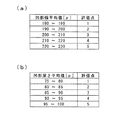
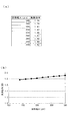
上記一参考実施形態においては、条件設定工程SA3において、凹部21の幅と深さの評価点を用いて上板基板14の加工条件を設定することとしたが、これに代えて、本発明の一実施形態に係るサーマルヘッドの製造方法は、凹部21の幅寸法および深さ寸法の測定値から、以下の式を用いて加工条件(上板基板14の適正な厚さc(μm))を設定する。
c=ln(e−0.0084×C ×(1−0.0005×(a−A)+(0.0055×b−0.69)×(b−B)))/−0.0084
ここで、A:凹部21の幅の基本設計値(μm)、B:凹部21の深さの基本設計値(μm)a:凹部21の幅の実際の測定値(μm)、b:凹部21の深さの実際の測定値(μm)
このようにして、上記式を用いて、上板基板14の適正な厚さ、すなわち、薄板化工程SA5における上板基板14の狙い値(μm)を設定することとしてもよい。
例えば、上記実施形態においては、大型の積層基板13単位で上板基板14を加工することとしたが、個々のサーマルヘッド10ごとに凹部21の寸法を求め、サーマルヘッド10ごとに設定された厚さに上板基板14を加工することとしてもよい。このようにすることで、品質がより均一性に優れたサーマルヘッド10を製造することができる。また、個々のサーマルヘッド10ごとに予め切り分けられた支持基板12および上板基板14を用いて、サーマルヘッド10を個別に製造することとしてもよい。
12 支持基板(第1基板)
14 上板基板(第2基板)
15 発熱抵抗体
21 凹部(溝部)
SA1 凹部形成工程(溝部形成工程)
SA2 測定工程
SA4 接合工程
SA5 薄板化工程
SA6 抵抗体形成工程
Claims (1)
- 平板状の第1基板および該第1基板に対して積層状態に配される平板状の第2基板の少なくとも一方の一表面に開口する溝部を形成する溝部形成工程と、
該溝部形成工程により形成された前記溝部の幅寸法および深さ寸法を測定する測定工程と、
該測定工程により測定された前記溝部の幅寸法および深さ寸法に基づいて前記第2基板の狙いの厚さを設定する条件設定工程と、
前記第1基板と前記第2基板とを前記溝部形成工程により形成された前記溝部の開口を閉塞するように積層状態に接合する接合工程と、
該接合工程により前記第1基板に接合された前記第2基板を、前記条件設定工程により設定された前記狙いの厚さまで薄板化する薄板化工程と、
該薄板化工程により薄板化された前記第2基板の表面における前記溝部に対向する領域に発熱抵抗体を形成する抵抗体形成工程とを含み、
前記条件設定工程が、前記溝部の幅寸法および深さ寸法の測定値から、以下の式を用いて前記狙いの厚さを設定するサーマルヘッドの製造方法。
c=ln(e−0.0084×C×(1−0.0005×(a−A)+(0.0055×b−0.69)×(b−B)))/−0.0084
ここで、c:発熱抵抗体から溝部までの狙いの距離(μm)、A:溝部の幅の基本設計値(μm)、B:溝部の深さの基本設計値(μm)、C:発熱抵抗体から溝部までの距離の基本設計値(μm)、a:溝部の幅の実際の測定値(μm)、b:溝部の深さの実際の測定値(μm)である。
Priority Applications (3)
| Application Number | Priority Date | Filing Date | Title |
|---|---|---|---|
| JP2010213291A JP5787247B2 (ja) | 2010-09-24 | 2010-09-24 | サーマルヘッドの製造方法 |
| US13/200,251 US20120073123A1 (en) | 2010-09-24 | 2011-09-21 | Method of manufacturing thermal head |
| CN201110305994.4A CN102555510B (zh) | 2010-09-24 | 2011-09-26 | 热头的制造方法 |
Applications Claiming Priority (1)
| Application Number | Priority Date | Filing Date | Title |
|---|---|---|---|
| JP2010213291A JP5787247B2 (ja) | 2010-09-24 | 2010-09-24 | サーマルヘッドの製造方法 |
Publications (2)
| Publication Number | Publication Date |
|---|---|
| JP2012066486A JP2012066486A (ja) | 2012-04-05 |
| JP5787247B2 true JP5787247B2 (ja) | 2015-09-30 |
Family
ID=45869171
Family Applications (1)
| Application Number | Title | Priority Date | Filing Date |
|---|---|---|---|
| JP2010213291A Expired - Fee Related JP5787247B2 (ja) | 2010-09-24 | 2010-09-24 | サーマルヘッドの製造方法 |
Country Status (3)
| Country | Link |
|---|---|
| US (1) | US20120073123A1 (ja) |
| JP (1) | JP5787247B2 (ja) |
| CN (1) | CN102555510B (ja) |
Families Citing this family (2)
| Publication number | Priority date | Publication date | Assignee | Title |
|---|---|---|---|---|
| JP5541660B2 (ja) * | 2009-08-06 | 2014-07-09 | セイコーインスツル株式会社 | サーマルヘッドの製造方法 |
| JP5943414B2 (ja) * | 2011-12-01 | 2016-07-05 | セイコーインスツル株式会社 | サーマルヘッドの製造方法 |
Family Cites Families (10)
| Publication number | Priority date | Publication date | Assignee | Title |
|---|---|---|---|---|
| JPH0299647U (ja) * | 1989-01-27 | 1990-08-08 | ||
| CN1086640C (zh) * | 1994-06-21 | 2002-06-26 | 罗姆股份有限公司 | 热打印头和用于打印头的基片以及该基片的制造方法 |
| JPH1178030A (ja) * | 1997-09-10 | 1999-03-23 | Brother Ind Ltd | インクジェットヘッドの製造方法 |
| JP2001239689A (ja) * | 2000-02-28 | 2001-09-04 | Ricoh Elemex Corp | サーマルヘッド、サーマルヘッドの調整方法および装置、サーマルヘッドの製造方法 |
| JP2007245667A (ja) * | 2006-03-17 | 2007-09-27 | Sony Corp | サーマルヘッド及びプリンタ装置 |
| JP4458054B2 (ja) * | 2006-03-17 | 2010-04-28 | ソニー株式会社 | サーマルヘッド及びプリンタ装置 |
| JP2007245668A (ja) * | 2006-03-17 | 2007-09-27 | Sony Corp | サーマルヘッド及びプリンタ装置 |
| JP5181111B2 (ja) * | 2007-10-03 | 2013-04-10 | セイコーインスツル株式会社 | 発熱抵抗素子部品およびサーマルプリンタ |
| US7768541B2 (en) * | 2007-10-23 | 2010-08-03 | Seiko Instruments Inc. | Heating resistor element, manufacturing method for the same, thermal head, and printer |
| JP2009119850A (ja) * | 2007-10-23 | 2009-06-04 | Seiko Instruments Inc | 発熱抵抗素子とその製造方法、サーマルヘッドおよびプリンタ |
-
2010
- 2010-09-24 JP JP2010213291A patent/JP5787247B2/ja not_active Expired - Fee Related
-
2011
- 2011-09-21 US US13/200,251 patent/US20120073123A1/en not_active Abandoned
- 2011-09-26 CN CN201110305994.4A patent/CN102555510B/zh not_active Expired - Fee Related
Also Published As
| Publication number | Publication date |
|---|---|
| JP2012066486A (ja) | 2012-04-05 |
| CN102555510A (zh) | 2012-07-11 |
| US20120073123A1 (en) | 2012-03-29 |
| CN102555510B (zh) | 2015-09-30 |
Similar Documents
| Publication | Publication Date | Title |
|---|---|---|
| JP5787247B2 (ja) | サーマルヘッドの製造方法 | |
| JP5421680B2 (ja) | サーマルヘッドの製造方法、サーマルヘッドおよびプリンタ | |
| JP5200256B2 (ja) | サーマルヘッドの製造方法 | |
| JP5787248B2 (ja) | サーマルヘッドの製造方法 | |
| JP5424387B2 (ja) | サーマルヘッドおよびサーマルヘッドの製造方法 | |
| JP5181111B2 (ja) | 発熱抵抗素子部品およびサーマルプリンタ | |
| JP5135585B2 (ja) | サーマルヘッドの製造方法 | |
| JP5541660B2 (ja) | サーマルヘッドの製造方法 | |
| CN102431312B (zh) | 热头、热敏打印机及热头的制造方法 | |
| JP5181107B2 (ja) | 発熱抵抗素子部品およびプリンタ | |
| JP5881098B2 (ja) | サーマルヘッドの製造方法 | |
| JP5181152B2 (ja) | サーマルヘッドの製造方法 | |
| JP2013139095A (ja) | サーマルヘッド、プリンタおよびサーマルヘッドの製造方法 | |
| JP5943414B2 (ja) | サーマルヘッドの製造方法 | |
| JP5765843B2 (ja) | サーマルヘッドの製造方法 | |
| JPH04257450A (ja) | インクジェットプリンターヘッドおよびその製造方法 | |
| JP2013116562A (ja) | サーマルヘッドの製造方法およびサーマルプリンタとその駆動方法 | |
| JP2009149023A (ja) | 発熱抵抗素子部品およびサーマルプリンタ | |
| JP5900849B2 (ja) | サーマルヘッド、プリンタおよびサーマルヘッドの製造方法 | |
| JP2001180025A (ja) | サーマルヘッド、及びこのサーマルヘッドの製造方法 | |
| JP2004188872A (ja) | サーマルヘッドの製造方法 | |
| JP2004188873A (ja) | サーマルヘッドの製造方法 |
Legal Events
| Date | Code | Title | Description |
|---|---|---|---|
| A621 | Written request for application examination |
Free format text: JAPANESE INTERMEDIATE CODE: A621 Effective date: 20130708 |
|
| A977 | Report on retrieval |
Free format text: JAPANESE INTERMEDIATE CODE: A971007 Effective date: 20140307 |
|
| A131 | Notification of reasons for refusal |
Free format text: JAPANESE INTERMEDIATE CODE: A131 Effective date: 20140318 |
|
| A521 | Request for written amendment filed |
Free format text: JAPANESE INTERMEDIATE CODE: A523 Effective date: 20140516 |
|
| A131 | Notification of reasons for refusal |
Free format text: JAPANESE INTERMEDIATE CODE: A131 Effective date: 20141209 |
|
| A521 | Request for written amendment filed |
Free format text: JAPANESE INTERMEDIATE CODE: A523 Effective date: 20150206 |
|
| TRDD | Decision of grant or rejection written | ||
| A01 | Written decision to grant a patent or to grant a registration (utility model) |
Free format text: JAPANESE INTERMEDIATE CODE: A01 Effective date: 20150630 |
|
| RD03 | Notification of appointment of power of attorney |
Free format text: JAPANESE INTERMEDIATE CODE: A7423 Effective date: 20150717 |
|
| A61 | First payment of annual fees (during grant procedure) |
Free format text: JAPANESE INTERMEDIATE CODE: A61 Effective date: 20150717 |
|
| R150 | Certificate of patent or registration of utility model |
Ref document number: 5787247 Country of ref document: JP Free format text: JAPANESE INTERMEDIATE CODE: R150 |
|
| R250 | Receipt of annual fees |
Free format text: JAPANESE INTERMEDIATE CODE: R250 |
|
| R250 | Receipt of annual fees |
Free format text: JAPANESE INTERMEDIATE CODE: R250 |
|
| R250 | Receipt of annual fees |
Free format text: JAPANESE INTERMEDIATE CODE: R250 |
|
| LAPS | Cancellation because of no payment of annual fees |