JP5809596B2 - 半導体装置およびその製造方法 - Google Patents
半導体装置およびその製造方法 Download PDFInfo
- Publication number
- JP5809596B2 JP5809596B2 JP2012106022A JP2012106022A JP5809596B2 JP 5809596 B2 JP5809596 B2 JP 5809596B2 JP 2012106022 A JP2012106022 A JP 2012106022A JP 2012106022 A JP2012106022 A JP 2012106022A JP 5809596 B2 JP5809596 B2 JP 5809596B2
- Authority
- JP
- Japan
- Prior art keywords
- film
- insulating film
- forming
- semiconductor device
- source electrode
- Prior art date
- Legal status (The legal status is an assumption and is not a legal conclusion. Google has not performed a legal analysis and makes no representation as to the accuracy of the status listed.)
- Expired - Fee Related
Links
Images

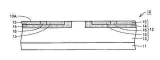
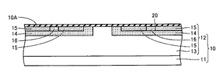


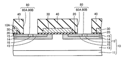


Classifications
-
- H—ELECTRICITY
- H10—SEMICONDUCTOR DEVICES; ELECTRIC SOLID-STATE DEVICES NOT OTHERWISE PROVIDED FOR
- H10D—INORGANIC ELECTRIC SEMICONDUCTOR DEVICES
- H10D30/00—Field-effect transistors [FET]
- H10D30/60—Insulated-gate field-effect transistors [IGFET]
- H10D30/64—Double-diffused metal-oxide semiconductor [DMOS] FETs
- H10D30/66—Vertical DMOS [VDMOS] FETs
- H10D30/667—Vertical DMOS [VDMOS] FETs having substrates comprising insulating layers, e.g. SOI-VDMOS transistors
-
- H—ELECTRICITY
- H10—SEMICONDUCTOR DEVICES; ELECTRIC SOLID-STATE DEVICES NOT OTHERWISE PROVIDED FOR
- H10W—GENERIC PACKAGES, INTERCONNECTIONS, CONNECTORS OR OTHER CONSTRUCTIONAL DETAILS OF DEVICES COVERED BY CLASS H10
- H10W20/00—Interconnections in chips, wafers or substrates
- H10W20/01—Manufacture or treatment
- H10W20/031—Manufacture or treatment of conductive parts of the interconnections
- H10W20/032—Manufacture or treatment of conductive parts of the interconnections of conductive barrier, adhesion or liner layers
-
- H—ELECTRICITY
- H10—SEMICONDUCTOR DEVICES; ELECTRIC SOLID-STATE DEVICES NOT OTHERWISE PROVIDED FOR
- H10D—INORGANIC ELECTRIC SEMICONDUCTOR DEVICES
- H10D12/00—Bipolar devices controlled by the field effect, e.g. insulated-gate bipolar transistors [IGBT]
- H10D12/01—Manufacture or treatment
- H10D12/031—Manufacture or treatment of IGBTs
-
- H—ELECTRICITY
- H10—SEMICONDUCTOR DEVICES; ELECTRIC SOLID-STATE DEVICES NOT OTHERWISE PROVIDED FOR
- H10D—INORGANIC ELECTRIC SEMICONDUCTOR DEVICES
- H10D12/00—Bipolar devices controlled by the field effect, e.g. insulated-gate bipolar transistors [IGBT]
- H10D12/01—Manufacture or treatment
- H10D12/031—Manufacture or treatment of IGBTs
- H10D12/032—Manufacture or treatment of IGBTs of vertical IGBTs
-
- H—ELECTRICITY
- H10—SEMICONDUCTOR DEVICES; ELECTRIC SOLID-STATE DEVICES NOT OTHERWISE PROVIDED FOR
- H10D—INORGANIC ELECTRIC SEMICONDUCTOR DEVICES
- H10D30/00—Field-effect transistors [FET]
- H10D30/01—Manufacture or treatment
- H10D30/021—Manufacture or treatment of FETs having insulated gates [IGFET]
- H10D30/028—Manufacture or treatment of FETs having insulated gates [IGFET] of double-diffused metal oxide semiconductor [DMOS] FETs
- H10D30/0291—Manufacture or treatment of FETs having insulated gates [IGFET] of double-diffused metal oxide semiconductor [DMOS] FETs of vertical DMOS [VDMOS] FETs
-
- H—ELECTRICITY
- H10—SEMICONDUCTOR DEVICES; ELECTRIC SOLID-STATE DEVICES NOT OTHERWISE PROVIDED FOR
- H10D—INORGANIC ELECTRIC SEMICONDUCTOR DEVICES
- H10D30/00—Field-effect transistors [FET]
- H10D30/60—Insulated-gate field-effect transistors [IGFET]
-
- H—ELECTRICITY
- H10—SEMICONDUCTOR DEVICES; ELECTRIC SOLID-STATE DEVICES NOT OTHERWISE PROVIDED FOR
- H10D—INORGANIC ELECTRIC SEMICONDUCTOR DEVICES
- H10D30/00—Field-effect transistors [FET]
- H10D30/60—Insulated-gate field-effect transistors [IGFET]
- H10D30/63—Vertical IGFETs
-
- H—ELECTRICITY
- H10—SEMICONDUCTOR DEVICES; ELECTRIC SOLID-STATE DEVICES NOT OTHERWISE PROVIDED FOR
- H10D—INORGANIC ELECTRIC SEMICONDUCTOR DEVICES
- H10D62/00—Semiconductor bodies, or regions thereof, of devices having potential barriers
- H10D62/80—Semiconductor bodies, or regions thereof, of devices having potential barriers characterised by the materials
- H10D62/83—Semiconductor bodies, or regions thereof, of devices having potential barriers characterised by the materials being Group IV materials, e.g. B-doped Si or undoped Ge
- H10D62/832—Semiconductor bodies, or regions thereof, of devices having potential barriers characterised by the materials being Group IV materials, e.g. B-doped Si or undoped Ge being Group IV materials comprising two or more elements, e.g. SiGe
- H10D62/8325—Silicon carbide
-
- H—ELECTRICITY
- H10—SEMICONDUCTOR DEVICES; ELECTRIC SOLID-STATE DEVICES NOT OTHERWISE PROVIDED FOR
- H10D—INORGANIC ELECTRIC SEMICONDUCTOR DEVICES
- H10D64/00—Electrodes of devices having potential barriers
- H10D64/01—Manufacture or treatment
- H10D64/013—Manufacture or treatment of electrodes having a conductor capacitively coupled to a semiconductor by an insulator
- H10D64/01302—Manufacture or treatment of electrodes having a conductor capacitively coupled to a semiconductor by an insulator the insulator being formed after the semiconductor body, the semiconductor being silicon
- H10D64/01304—Manufacture or treatment of electrodes having a conductor capacitively coupled to a semiconductor by an insulator the insulator being formed after the semiconductor body, the semiconductor being silicon characterised by the conductor
-
- H—ELECTRICITY
- H10—SEMICONDUCTOR DEVICES; ELECTRIC SOLID-STATE DEVICES NOT OTHERWISE PROVIDED FOR
- H10D—INORGANIC ELECTRIC SEMICONDUCTOR DEVICES
- H10D64/00—Electrodes of devices having potential barriers
- H10D64/01—Manufacture or treatment
- H10D64/013—Manufacture or treatment of electrodes having a conductor capacitively coupled to a semiconductor by an insulator
- H10D64/01366—Manufacture or treatment of electrodes having a conductor capacitively coupled to a semiconductor by an insulator the semiconductor being silicon carbide
-
- H—ELECTRICITY
- H10—SEMICONDUCTOR DEVICES; ELECTRIC SOLID-STATE DEVICES NOT OTHERWISE PROVIDED FOR
- H10D—INORGANIC ELECTRIC SEMICONDUCTOR DEVICES
- H10D64/00—Electrodes of devices having potential barriers
- H10D64/60—Electrodes characterised by their materials
- H10D64/62—Electrodes ohmically coupled to a semiconductor
-
- H—ELECTRICITY
- H10—SEMICONDUCTOR DEVICES; ELECTRIC SOLID-STATE DEVICES NOT OTHERWISE PROVIDED FOR
- H10P—GENERIC PROCESSES OR APPARATUS FOR THE MANUFACTURE OR TREATMENT OF DEVICES COVERED BY CLASS H10
- H10P30/00—Ion implantation into wafers, substrates or parts of devices
- H10P30/20—Ion implantation into wafers, substrates or parts of devices into semiconductor materials, e.g. for doping
- H10P30/202—Ion implantation into wafers, substrates or parts of devices into semiconductor materials, e.g. for doping characterised by the semiconductor materials
- H10P30/204—Ion implantation into wafers, substrates or parts of devices into semiconductor materials, e.g. for doping characterised by the semiconductor materials into Group IV semiconductors
- H10P30/2042—Ion implantation into wafers, substrates or parts of devices into semiconductor materials, e.g. for doping characterised by the semiconductor materials into Group IV semiconductors into crystalline silicon carbide
-
- H—ELECTRICITY
- H10—SEMICONDUCTOR DEVICES; ELECTRIC SOLID-STATE DEVICES NOT OTHERWISE PROVIDED FOR
- H10P—GENERIC PROCESSES OR APPARATUS FOR THE MANUFACTURE OR TREATMENT OF DEVICES COVERED BY CLASS H10
- H10P30/00—Ion implantation into wafers, substrates or parts of devices
- H10P30/20—Ion implantation into wafers, substrates or parts of devices into semiconductor materials, e.g. for doping
- H10P30/21—Ion implantation into wafers, substrates or parts of devices into semiconductor materials, e.g. for doping of electrically active species
-
- H—ELECTRICITY
- H10—SEMICONDUCTOR DEVICES; ELECTRIC SOLID-STATE DEVICES NOT OTHERWISE PROVIDED FOR
- H10P—GENERIC PROCESSES OR APPARATUS FOR THE MANUFACTURE OR TREATMENT OF DEVICES COVERED BY CLASS H10
- H10P30/00—Ion implantation into wafers, substrates or parts of devices
- H10P30/20—Ion implantation into wafers, substrates or parts of devices into semiconductor materials, e.g. for doping
- H10P30/28—Ion implantation into wafers, substrates or parts of devices into semiconductor materials, e.g. for doping characterised by an annealing step, e.g. for activation of dopants
-
- H—ELECTRICITY
- H10—SEMICONDUCTOR DEVICES; ELECTRIC SOLID-STATE DEVICES NOT OTHERWISE PROVIDED FOR
- H10W—GENERIC PACKAGES, INTERCONNECTIONS, CONNECTORS OR OTHER CONSTRUCTIONAL DETAILS OF DEVICES COVERED BY CLASS H10
- H10W20/00—Interconnections in chips, wafers or substrates
- H10W20/01—Manufacture or treatment
- H10W20/031—Manufacture or treatment of conductive parts of the interconnections
- H10W20/032—Manufacture or treatment of conductive parts of the interconnections of conductive barrier, adhesion or liner layers
- H10W20/033—Manufacture or treatment of conductive parts of the interconnections of conductive barrier, adhesion or liner layers in openings in dielectrics
- H10W20/034—Manufacture or treatment of conductive parts of the interconnections of conductive barrier, adhesion or liner layers in openings in dielectrics bottomless barrier, adhesion or liner layers
-
- H—ELECTRICITY
- H10—SEMICONDUCTOR DEVICES; ELECTRIC SOLID-STATE DEVICES NOT OTHERWISE PROVIDED FOR
- H10W—GENERIC PACKAGES, INTERCONNECTIONS, CONNECTORS OR OTHER CONSTRUCTIONAL DETAILS OF DEVICES COVERED BY CLASS H10
- H10W20/00—Interconnections in chips, wafers or substrates
- H10W20/01—Manufacture or treatment
- H10W20/031—Manufacture or treatment of conductive parts of the interconnections
- H10W20/032—Manufacture or treatment of conductive parts of the interconnections of conductive barrier, adhesion or liner layers
- H10W20/047—Manufacture or treatment of conductive parts of the interconnections of conductive barrier, adhesion or liner layers by introducing additional elements therein
Landscapes
- Electrodes Of Semiconductors (AREA)
- Internal Circuitry In Semiconductor Integrated Circuit Devices (AREA)
Priority Applications (5)
| Application Number | Priority Date | Filing Date | Title |
|---|---|---|---|
| JP2012106022A JP5809596B2 (ja) | 2012-05-07 | 2012-05-07 | 半導体装置およびその製造方法 |
| EP13788394.8A EP2849231B1 (fr) | 2012-05-07 | 2013-03-29 | Dispositif semi-conducteur et procédé de fabrication de celui-ci |
| CN201380015255.9A CN104170093B (zh) | 2012-05-07 | 2013-03-29 | 半导体器件及其制造方法 |
| PCT/JP2013/059491 WO2013168484A1 (fr) | 2012-05-07 | 2013-03-29 | Dispositif semi-conducteur et procédé de fabrication de celui-ci |
| US13/856,950 US9177856B2 (en) | 2012-05-07 | 2013-04-04 | Semiconductor device and method for manufacturing same |
Applications Claiming Priority (1)
| Application Number | Priority Date | Filing Date | Title |
|---|---|---|---|
| JP2012106022A JP5809596B2 (ja) | 2012-05-07 | 2012-05-07 | 半導体装置およびその製造方法 |
Publications (2)
| Publication Number | Publication Date |
|---|---|
| JP2013235893A JP2013235893A (ja) | 2013-11-21 |
| JP5809596B2 true JP5809596B2 (ja) | 2015-11-11 |
Family
ID=49511866
Family Applications (1)
| Application Number | Title | Priority Date | Filing Date |
|---|---|---|---|
| JP2012106022A Expired - Fee Related JP5809596B2 (ja) | 2012-05-07 | 2012-05-07 | 半導体装置およびその製造方法 |
Country Status (5)
| Country | Link |
|---|---|
| US (1) | US9177856B2 (fr) |
| EP (1) | EP2849231B1 (fr) |
| JP (1) | JP5809596B2 (fr) |
| CN (1) | CN104170093B (fr) |
| WO (1) | WO2013168484A1 (fr) |
Families Citing this family (10)
| Publication number | Priority date | Publication date | Assignee | Title |
|---|---|---|---|---|
| JP2014038899A (ja) | 2012-08-13 | 2014-02-27 | Sumitomo Electric Ind Ltd | 炭化珪素半導体装置およびその製造方法 |
| JP5949305B2 (ja) * | 2012-08-13 | 2016-07-06 | 住友電気工業株式会社 | 炭化珪素半導体装置の製造方法 |
| JP6068918B2 (ja) | 2012-10-15 | 2017-01-25 | 住友電気工業株式会社 | 半導体装置およびその製造方法 |
| JP6183200B2 (ja) * | 2013-12-16 | 2017-08-23 | 住友電気工業株式会社 | 炭化珪素半導体装置およびその製造方法 |
| JP6435686B2 (ja) * | 2014-07-23 | 2018-12-12 | 富士電機株式会社 | 炭化珪素半導体装置の製造方法および炭化珪素半導体装置 |
| JP6191587B2 (ja) * | 2014-12-08 | 2017-09-06 | トヨタ自動車株式会社 | 半導体装置 |
| CN109300947B (zh) * | 2018-09-28 | 2021-09-07 | 京东方科技集团股份有限公司 | 柔性显示基板及其制造方法、显示装置 |
| US11075276B2 (en) | 2018-10-08 | 2021-07-27 | Applied Materials, Inc. | Methods and apparatus for n-type metal oxide semiconductor (NMOS) metal gate materials using atomic layer deposition (ALD) processes with metal based precursors |
| JP2021012996A (ja) * | 2019-07-09 | 2021-02-04 | 株式会社豊田中央研究所 | 半導体装置 |
| US20240313079A1 (en) * | 2023-03-16 | 2024-09-19 | Applied Materials, Inc. | Semiconductor devices containing bi-metallic silicide with reduced contact resistivity |
Family Cites Families (14)
| Publication number | Priority date | Publication date | Assignee | Title |
|---|---|---|---|---|
| JPH07202185A (ja) * | 1993-12-28 | 1995-08-04 | Sharp Corp | 縦型mosトランジスタの製造方法 |
| JP4003296B2 (ja) | 1998-06-22 | 2007-11-07 | 株式会社デンソー | 炭化珪素半導体装置及びその製造方法 |
| US6391785B1 (en) | 1999-08-24 | 2002-05-21 | Interuniversitair Microelektronica Centrum (Imec) | Method for bottomless deposition of barrier layers in integrated circuit metallization schemes |
| JP3559971B2 (ja) | 2001-12-11 | 2004-09-02 | 日産自動車株式会社 | 炭化珪素半導体装置およびその製造方法 |
| JP4002916B2 (ja) * | 2003-10-22 | 2007-11-07 | 松下電器産業株式会社 | 半導体装置及びその製造方法 |
| CN100377357C (zh) * | 2003-10-22 | 2008-03-26 | 松下电器产业株式会社 | 半导体装置及其制造方法 |
| US8629490B2 (en) | 2006-03-31 | 2014-01-14 | Semiconductor Energy Laboratory Co., Ltd. | Nonvolatile semiconductor storage device with floating gate electrode and control gate electrode |
| WO2009013886A1 (fr) * | 2007-07-20 | 2009-01-29 | Panasonic Corporation | Dispositif semi-conducteur au carbure de silicium et son procédé de fabrication |
| JP5157843B2 (ja) | 2007-12-04 | 2013-03-06 | 住友電気工業株式会社 | 炭化ケイ素半導体装置およびその製造方法 |
| JP2010238738A (ja) * | 2009-03-30 | 2010-10-21 | Toshiba Corp | 半導体装置および半導体装置の製造方法 |
| JP4858791B2 (ja) * | 2009-05-22 | 2012-01-18 | 住友電気工業株式会社 | 半導体装置およびその製造方法 |
| JP5860580B2 (ja) * | 2009-05-25 | 2016-02-16 | 日産自動車株式会社 | 半導体装置及びその製造方法 |
| JP5581642B2 (ja) * | 2009-10-05 | 2014-09-03 | 住友電気工業株式会社 | 半導体装置の製造方法 |
| JP2013235895A (ja) * | 2012-05-07 | 2013-11-21 | Sumitomo Electric Ind Ltd | 半導体装置およびその製造方法 |
-
2012
- 2012-05-07 JP JP2012106022A patent/JP5809596B2/ja not_active Expired - Fee Related
-
2013
- 2013-03-29 CN CN201380015255.9A patent/CN104170093B/zh not_active Expired - Fee Related
- 2013-03-29 WO PCT/JP2013/059491 patent/WO2013168484A1/fr not_active Ceased
- 2013-03-29 EP EP13788394.8A patent/EP2849231B1/fr active Active
- 2013-04-04 US US13/856,950 patent/US9177856B2/en active Active
Also Published As
| Publication number | Publication date |
|---|---|
| US9177856B2 (en) | 2015-11-03 |
| EP2849231A1 (fr) | 2015-03-18 |
| EP2849231B1 (fr) | 2019-10-30 |
| CN104170093A (zh) | 2014-11-26 |
| CN104170093B (zh) | 2018-06-01 |
| US20130292703A1 (en) | 2013-11-07 |
| EP2849231A4 (fr) | 2015-12-23 |
| JP2013235893A (ja) | 2013-11-21 |
| WO2013168484A1 (fr) | 2013-11-14 |
Similar Documents
| Publication | Publication Date | Title |
|---|---|---|
| JP5809596B2 (ja) | 半導体装置およびその製造方法 | |
| CN101964357B (zh) | 半导体装置及半导体装置的制造方法 | |
| JP2013235895A (ja) | 半導体装置およびその製造方法 | |
| JP5708550B2 (ja) | 炭化珪素半導体装置およびその製造方法 | |
| KR20130109168A (ko) | 탄화규소 반도체 장치의 제조 방법 | |
| JP2015076592A (ja) | 炭化珪素半導体装置およびその製造方法 | |
| JPWO2012137412A1 (ja) | 半導体装置 | |
| JP2014175470A (ja) | 炭化珪素半導体装置の製造方法 | |
| CN104995739B (zh) | 碳化硅半导体器件 | |
| WO2013088855A1 (fr) | Procédé permettant de fabriquer un dispositif semi-conducteur | |
| JP2015201604A (ja) | 炭化珪素半導体装置およびその製造方法 | |
| JP6068918B2 (ja) | 半導体装置およびその製造方法 | |
| JP2015204409A (ja) | 炭化珪素半導体装置およびその製造方法 | |
| JP5704003B2 (ja) | 半導体装置の製造方法 | |
| JP2016143788A (ja) | 炭化珪素半導体装置の製造方法 | |
| JP5721868B2 (ja) | 半導体装置およびその製造方法 | |
| JP2013093493A (ja) | 半導体装置の製造方法 | |
| JP6229443B2 (ja) | 炭化珪素半導体装置およびその製造方法 | |
| JP5991629B2 (ja) | 半導体装置および半導体装置の製造方法 |
Legal Events
| Date | Code | Title | Description |
|---|---|---|---|
| A621 | Written request for application examination |
Free format text: JAPANESE INTERMEDIATE CODE: A621 Effective date: 20150223 |
|
| A131 | Notification of reasons for refusal |
Free format text: JAPANESE INTERMEDIATE CODE: A131 Effective date: 20150602 |
|
| A521 | Request for written amendment filed |
Free format text: JAPANESE INTERMEDIATE CODE: A523 Effective date: 20150710 |
|
| TRDD | Decision of grant or rejection written | ||
| A01 | Written decision to grant a patent or to grant a registration (utility model) |
Free format text: JAPANESE INTERMEDIATE CODE: A01 Effective date: 20150825 |
|
| A61 | First payment of annual fees (during grant procedure) |
Free format text: JAPANESE INTERMEDIATE CODE: A61 Effective date: 20150911 |
|
| R150 | Certificate of patent or registration of utility model |
Ref document number: 5809596 Country of ref document: JP Free format text: JAPANESE INTERMEDIATE CODE: R150 |
|
| R250 | Receipt of annual fees |
Free format text: JAPANESE INTERMEDIATE CODE: R250 |
|
| R250 | Receipt of annual fees |
Free format text: JAPANESE INTERMEDIATE CODE: R250 |
|
| R250 | Receipt of annual fees |
Free format text: JAPANESE INTERMEDIATE CODE: R250 |
|
| R250 | Receipt of annual fees |
Free format text: JAPANESE INTERMEDIATE CODE: R250 |
|
| R250 | Receipt of annual fees |
Free format text: JAPANESE INTERMEDIATE CODE: R250 |
|
| R250 | Receipt of annual fees |
Free format text: JAPANESE INTERMEDIATE CODE: R250 |
|
| LAPS | Cancellation because of no payment of annual fees |