JP5873669B2 - 2フォトン吸収を用いたレーザ・アシステッド・デバイス・オルタレーション - Google Patents
2フォトン吸収を用いたレーザ・アシステッド・デバイス・オルタレーション Download PDFInfo
- Publication number
- JP5873669B2 JP5873669B2 JP2011195895A JP2011195895A JP5873669B2 JP 5873669 B2 JP5873669 B2 JP 5873669B2 JP 2011195895 A JP2011195895 A JP 2011195895A JP 2011195895 A JP2011195895 A JP 2011195895A JP 5873669 B2 JP5873669 B2 JP 5873669B2
- Authority
- JP
- Japan
- Prior art keywords
- dut
- laser light
- light pulse
- laser
- tester
- Prior art date
- Legal status (The legal status is an assumption and is not a legal conclusion. Google has not performed a legal analysis and makes no representation as to the accuracy of the status listed.)
- Expired - Fee Related
Links
Images

Classifications
-
- G—PHYSICS
- G01—MEASURING; TESTING
- G01R—MEASURING ELECTRIC VARIABLES; MEASURING MAGNETIC VARIABLES
- G01R31/00—Arrangements for testing electric properties; Arrangements for locating electric faults; Arrangements for electrical testing characterised by what is being tested not provided for elsewhere
- G01R31/28—Testing of electronic circuits, e.g. by signal tracer
- G01R31/302—Contactless testing
- G01R31/308—Contactless testing using non-ionising electromagnetic radiation, e.g. optical radiation
- G01R31/311—Contactless testing using non-ionising electromagnetic radiation, e.g. optical radiation of integrated circuits
-
- G—PHYSICS
- G01—MEASURING; TESTING
- G01N—INVESTIGATING OR ANALYSING MATERIALS BY DETERMINING THEIR CHEMICAL OR PHYSICAL PROPERTIES
- G01N21/00—Investigating or analysing materials by the use of optical means, i.e. using sub-millimetre waves, infrared, visible or ultraviolet light
- G01N21/62—Systems in which the material investigated is excited whereby it emits light or causes a change in wavelength of the incident light
- G01N21/63—Systems in which the material investigated is excited whereby it emits light or causes a change in wavelength of the incident light optically excited
- G01N21/636—Systems in which the material investigated is excited whereby it emits light or causes a change in wavelength of the incident light optically excited using an arrangement of pump beam and probe beam; using the measurement of optical non-linear properties
-
- G—PHYSICS
- G01—MEASURING; TESTING
- G01R—MEASURING ELECTRIC VARIABLES; MEASURING MAGNETIC VARIABLES
- G01R31/00—Arrangements for testing electric properties; Arrangements for locating electric faults; Arrangements for electrical testing characterised by what is being tested not provided for elsewhere
- G01R31/28—Testing of electronic circuits, e.g. by signal tracer
- G01R31/302—Contactless testing
- G01R31/303—Contactless testing of integrated circuits
Landscapes
- Physics & Mathematics (AREA)
- Engineering & Computer Science (AREA)
- Health & Medical Sciences (AREA)
- General Physics & Mathematics (AREA)
- Computer Hardware Design (AREA)
- Microelectronics & Electronic Packaging (AREA)
- General Engineering & Computer Science (AREA)
- Computer Vision & Pattern Recognition (AREA)
- Electromagnetism (AREA)
- Toxicology (AREA)
- Nuclear Medicine, Radiotherapy & Molecular Imaging (AREA)
- General Health & Medical Sciences (AREA)
- Nonlinear Science (AREA)
- Life Sciences & Earth Sciences (AREA)
- Chemical & Material Sciences (AREA)
- Analytical Chemistry (AREA)
- Biochemistry (AREA)
- Optics & Photonics (AREA)
- Immunology (AREA)
- Pathology (AREA)
- Tests Of Electronic Circuits (AREA)
- Testing Or Measuring Of Semiconductors Or The Like (AREA)
- Testing Of Individual Semiconductor Devices (AREA)
- Lasers (AREA)
- Optical Modulation, Optical Deflection, Nonlinear Optics, Optical Demodulation, Optical Logic Elements (AREA)
Description
Claims (11)
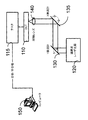
- テスタによって刺激が与えられるテスト対象のデバイス(DUT)における故障位置測定を行うシステムであって、
フェムト秒パルス幅及びシリコンのバンドギャップより長い波長を有するレーザ光パルスを供給するレーザ光源と、
前記レーザ光パルスを受け取り、前記レーザ光パルスを前記DUTの関心領域に送出する光学素子と、
前記テスタから同期信号を受信し、前記同期信号に従って前記レーザ光源のタイミングを制御するタイミング電子回路とを備え、
前記レーザ光パルスのパルス幅及び波長は、前記DUTにおいて2フォトン吸収を生じさせるように選択され、
前記タイミング電子回路は、前記DUTに対する2フォトン効果の量を変化させるために前記レーザ光パルスのタイミングを制御して、前記DUTのスイッチング時間を増加又は減少させ、前記DUTにおける故障の重大度の決定を支援する
システム。 - 前記レーザ光源は、1250nmと1550nmとの間の波長のレーザ光パルスを供給する
請求項1のシステム。 - 前記レーザ光源は、約100フェムト秒のパルス幅のレーザ光パルスを供給する
請求項2のシステム。 - 前記光学素子は、レーザ走査顕微鏡(LSM)を含む
請求項2のシステム。 - 前記光学素子は、更にソリッドイマージョンレンズを含む
請求項4のシステム。 - テスタからのテストベクトルによって刺激が与えられるテスト対象のデバイス(DUT)のスイッチング時間を変更する方法であって、
フェムト秒パルス幅及びシリコンのバンドギャップより長い波長を有するレーザ光パルスを生成し、
前記レーザ光パルスを前記DUTの関心領域に送出し、
前記テスタからの同期信号に従って、前記レーザ光パルスを生成するレーザ光源のタイミングを制御し、
前記レーザ光パルスのパルス幅及び波長は、前記DUTにおいて2フォトン吸収を生じさせるように選択され、
前記方法は、更に、前記DUTに対する2フォトン効果の量を変化させるために前記レーザ光パルスのタイミングを変更して、前記DUTのスイッチング時間を増加又は減少させ、前記DUTにおける故障の重大度の決定を支援する
方法。 - 前記レーザ光パルスは、1250nmと1550nmとの間の波長を有する
請求項6の方法。 - 前記レーザ光パルスは、約100フェムト秒のパルス幅を有する
請求項6の方法。 - テスタによって刺激が与えられるテスト対象のデバイス(DUT)をテストする方法であって、
前記テスタからのテストベクトルの第1の組を前記DUTに適用して、前記DUTの限界の設定を決定し、
前記DUTの前記限界の設定に従って、前記テスタのテストベクトルの第2の組の電圧及び周波数を設定し、
前記テスタからのテストベクトルの前記第2の組を前記DUTに繰り返し適用し、
前記テスタから同期信号を受け取り、
前記同期信号をレーザ光源に適用して、フェムト秒パルス幅及びシリコンのバンドギャップより長い波長を有するレーザ光パルスを受け取り、
前記レーザ光パルスを前記DUTの関心領域に適用して、前記DUTのスイッチング時間を増加又は減少させ、
前記DUTの出力を監視して、故障の位置を決定し、
前記DUTに対する2フォトン効果の量を変化させるために前記レーザ光パルスのタイミングを変更して、前記DUTのスイッチング時間を増加又は減少させ、前記DUTにおける故障の重大度の決定を支援する
方法。 - 前記DUTの出力の監視は、各時点において前記DUTの合否を監視し、前記合否の結果をその時点の前記レーザ光パルスが照射する場所に関連付けることを含む
請求項9の方法。 - 前記限界の設定の決定は、テストベクトルの電圧及び周波数を、前記DUTが前記テストに不合格になる寸前になるように、又は前記テストにちょうど不合格になるように決定することを含む
請求項9の方法。
Applications Claiming Priority (2)
| Application Number | Priority Date | Filing Date | Title |
|---|---|---|---|
| US38102310P | 2010-09-08 | 2010-09-08 | |
| US61/381,023 | 2010-09-08 |
Publications (2)
| Publication Number | Publication Date |
|---|---|
| JP2012058247A JP2012058247A (ja) | 2012-03-22 |
| JP5873669B2 true JP5873669B2 (ja) | 2016-03-01 |
Family
ID=44651256
Family Applications (1)
| Application Number | Title | Priority Date | Filing Date |
|---|---|---|---|
| JP2011195895A Expired - Fee Related JP5873669B2 (ja) | 2010-09-08 | 2011-09-08 | 2フォトン吸収を用いたレーザ・アシステッド・デバイス・オルタレーション |
Country Status (6)
| Country | Link |
|---|---|
| US (1) | US8860447B2 (ja) |
| EP (1) | EP2428807A3 (ja) |
| JP (1) | JP5873669B2 (ja) |
| CN (1) | CN102401632B (ja) |
| SG (3) | SG10201607265WA (ja) |
| TW (1) | TWI440869B (ja) |
Cited By (3)
| Publication number | Priority date | Publication date | Assignee | Title |
|---|---|---|---|---|
| US10191111B2 (en) | 2013-03-24 | 2019-01-29 | Dcg Systems, Inc. | Synchronized pulsed LADA for the simultaneous acquisition of timing diagrams and laser-induced upsets |
| US10209274B2 (en) | 2010-09-08 | 2019-02-19 | Fei Efa, Inc. | Laser-assisted device alteration using synchronized laser pulses |
| US10352995B1 (en) | 2018-02-28 | 2019-07-16 | Nxp Usa, Inc. | System and method of multiplexing laser triggers and optically selecting multiplexed laser pulses for laser assisted device alteration testing of semiconductor device |
Families Citing this family (10)
| Publication number | Priority date | Publication date | Assignee | Title |
|---|---|---|---|---|
| TWI440869B (zh) | 2010-09-08 | 2014-06-11 | Dcg Systems Inc | 使用雙光子吸收的雷射輔助裝置修改 |
| JP6200947B2 (ja) * | 2012-05-16 | 2017-09-20 | ディーシージー システムズ、 インコーポレイテッドDcg Systems Inc. | 同期レーザパルスを用いたレーザ・アシステッド・デバイス・オルタレーション |
| JP6317321B2 (ja) * | 2013-02-19 | 2018-04-25 | 浜松ホトニクス株式会社 | 電界集中位置観察装置および電界集中位置観察方法 |
| TWI619954B (zh) * | 2014-10-16 | 2018-04-01 | Dcg系統公司 | 雷射電壓測試系統與方法 |
| JP6820184B2 (ja) * | 2016-10-26 | 2021-01-27 | 浜松ホトニクス株式会社 | 半導体デバイス検査方法及び半導体デバイス検査装置 |
| JP6927690B2 (ja) | 2016-11-04 | 2021-09-01 | 浜松ホトニクス株式会社 | 半導体デバイス検査装置及び半導体デバイス検査方法 |
| US10782343B2 (en) | 2018-04-17 | 2020-09-22 | Nxp Usa, Inc. | Digital tests with radiation induced upsets |
| CN110780180A (zh) * | 2019-10-25 | 2020-02-11 | 长江存储科技有限责任公司 | 芯片测试装置及系统 |
| CN113162694B (zh) * | 2021-02-23 | 2022-12-20 | 复旦大学 | 一种光子辅助矢量毫米波信号产生系统 |
| US20220187362A1 (en) * | 2022-02-07 | 2022-06-16 | Intel Corporation | Laser-induced hot carrier injection (hci) for accelerated aging of integrated circuits |
Family Cites Families (21)
| Publication number | Priority date | Publication date | Assignee | Title |
|---|---|---|---|---|
| US5095262A (en) | 1988-09-01 | 1992-03-10 | Photon Dynamics, Inc. | Electro-optic sampling system clock and stimulus pattern generator |
| JP3352239B2 (ja) * | 1994-08-19 | 2002-12-03 | 浜松ホトニクス株式会社 | 電圧測定装置 |
| US6316950B1 (en) * | 1997-05-15 | 2001-11-13 | Lucent Technologies Inc. | Method and apparatus for imaging semiconductor devices |
| US6400165B1 (en) * | 2000-02-02 | 2002-06-04 | Lucent Technologies Inc. | Ultra-fast probe |
| US6621275B2 (en) * | 2001-11-28 | 2003-09-16 | Optonics Inc. | Time resolved non-invasive diagnostics system |
| US6882170B2 (en) * | 2002-12-05 | 2005-04-19 | Intel Corporation | Device speed alteration by electron-hole pair injection and device heating |
| JP4421319B2 (ja) * | 2004-02-13 | 2010-02-24 | 独立行政法人科学技術振興機構 | レーザ装置及びレーザ発振方法 |
| US7516379B2 (en) * | 2004-04-06 | 2009-04-07 | Avago Technologies General Ip (Singapore) Pte. Ltd. | Circuit and method for comparing circuit performance between functional and AC scan testing in an integrated circuit (IC) |
| JP4683869B2 (ja) * | 2004-07-08 | 2011-05-18 | 独立行政法人理化学研究所 | 半導体デバイスの故障診断方法と装置 |
| US7450245B2 (en) | 2005-06-29 | 2008-11-11 | Dcg Systems, Inc. | Method and apparatus for measuring high-bandwidth electrical signals using modulation in an optical probing system |
| US9130344B2 (en) | 2006-01-23 | 2015-09-08 | Raydiance, Inc. | Automated laser tuning |
| US8072589B2 (en) * | 2007-01-18 | 2011-12-06 | Dcg Systems, Inc. | System and method for photoemission-based defect detection |
| JP2008300486A (ja) * | 2007-05-30 | 2008-12-11 | Toshiba Corp | 半導体装置の検査システム、検査方法、及び検査装置 |
| FR2919402B1 (fr) * | 2007-07-23 | 2009-10-30 | Eads Europ Aeronautic Defence | Procede de test d'une application logicielle. |
| US20090147255A1 (en) * | 2007-12-07 | 2009-06-11 | Erington Kent B | Method for testing a semiconductor device and a semiconductor device testing system |
| TWI424479B (zh) | 2008-02-29 | 2014-01-21 | Ind Tech Res Inst | 利用飛秒雷射圖案化多晶氧化銦錫之方法 |
| JP2010181288A (ja) * | 2009-02-05 | 2010-08-19 | Renesas Electronics Corp | 半導体集積回路の解析装置及び解析方法 |
| JP2011075441A (ja) * | 2009-09-30 | 2011-04-14 | Hamamatsu Photonics Kk | 半導体デバイス故障解析装置 |
| TWI440869B (zh) | 2010-09-08 | 2014-06-11 | Dcg Systems Inc | 使用雙光子吸收的雷射輔助裝置修改 |
| US9201096B2 (en) | 2010-09-08 | 2015-12-01 | Dcg Systems, Inc. | Laser-assisted device alteration using synchronized laser pulses |
| JP6200947B2 (ja) | 2012-05-16 | 2017-09-20 | ディーシージー システムズ、 インコーポレイテッドDcg Systems Inc. | 同期レーザパルスを用いたレーザ・アシステッド・デバイス・オルタレーション |
-
2011
- 2011-09-07 TW TW100132283A patent/TWI440869B/zh not_active IP Right Cessation
- 2011-09-07 EP EP11180399.5A patent/EP2428807A3/en not_active Withdrawn
- 2011-09-08 SG SG10201607265WA patent/SG10201607265WA/en unknown
- 2011-09-08 US US13/228,369 patent/US8860447B2/en active Active
- 2011-09-08 SG SG10201507213UA patent/SG10201507213UA/en unknown
- 2011-09-08 CN CN201110319332.2A patent/CN102401632B/zh active Active
- 2011-09-08 SG SG2011064391A patent/SG179362A1/en unknown
- 2011-09-08 JP JP2011195895A patent/JP5873669B2/ja not_active Expired - Fee Related
Cited By (5)
| Publication number | Priority date | Publication date | Assignee | Title |
|---|---|---|---|---|
| US10209274B2 (en) | 2010-09-08 | 2019-02-19 | Fei Efa, Inc. | Laser-assisted device alteration using synchronized laser pulses |
| US11353479B2 (en) | 2010-09-08 | 2022-06-07 | Fei Efa, Inc. | Laser-assisted device alteration using synchronized laser pulses |
| US10191111B2 (en) | 2013-03-24 | 2019-01-29 | Dcg Systems, Inc. | Synchronized pulsed LADA for the simultaneous acquisition of timing diagrams and laser-induced upsets |
| US11047906B2 (en) | 2013-03-24 | 2021-06-29 | Dcg Systems, Inc. | Synchronized pulsed LADA for the simultaneous acquisition of timing diagrams and laser-induced upsets |
| US10352995B1 (en) | 2018-02-28 | 2019-07-16 | Nxp Usa, Inc. | System and method of multiplexing laser triggers and optically selecting multiplexed laser pulses for laser assisted device alteration testing of semiconductor device |
Also Published As
| Publication number | Publication date |
|---|---|
| CN102401632B (zh) | 2017-03-01 |
| US20120056626A1 (en) | 2012-03-08 |
| SG10201607265WA (en) | 2016-10-28 |
| US8860447B2 (en) | 2014-10-14 |
| SG10201507213UA (en) | 2015-10-29 |
| EP2428807A3 (en) | 2014-10-29 |
| EP2428807A2 (en) | 2012-03-14 |
| JP2012058247A (ja) | 2012-03-22 |
| SG179362A1 (en) | 2012-04-27 |
| CN102401632A (zh) | 2012-04-04 |
| TWI440869B (zh) | 2014-06-11 |
| TW201211561A (en) | 2012-03-16 |
Similar Documents
| Publication | Publication Date | Title |
|---|---|---|
| JP5873669B2 (ja) | 2フォトン吸収を用いたレーザ・アシステッド・デバイス・オルタレーション | |
| US11353479B2 (en) | Laser-assisted device alteration using synchronized laser pulses | |
| US9098892B2 (en) | Lock in thermal laser stimulation through one side of the device while acquiring lock-in thermal emission images on the opposite side | |
| JP6200947B2 (ja) | 同期レーザパルスを用いたレーザ・アシステッド・デバイス・オルタレーション | |
| US6549022B1 (en) | Apparatus and method for analyzing functional failures in integrated circuits | |
| TWI593983B (zh) | 可同時取得時序圖與雷射引發擾動,具同步化脈衝的雷射輔助裝置修改系統與方法 | |
| KR101777031B1 (ko) | 반도체 디바이스 검사 장치 및 반도체 디바이스 검사 방법 | |
| US8941824B2 (en) | Semiconductor inspection method and semiconductor inspection apparatus | |
| JP4001373B2 (ja) | 集積回路断線検査方法と装置 | |
| CN108369255A (zh) | 可调谐波长电子光学分析器 | |
| Dickson et al. | Picosecond Time-Resolved LADA Integrated with a Solid Immersion Lens on a Laser Scanning Microscope | |
| US6882170B2 (en) | Device speed alteration by electron-hole pair injection and device heating | |
| Andrus et al. | A Rapid, Pulsed Laser Testing Approach for Single Event Latch-Up Screening | |
| Pouget et al. | Picosecond single-photon and femtosecond two-photon pulsed laser stimulation for IC characterization and failure analysis | |
| Serrels et al. | Two-photon X-Variation mapping based on a diode-pumped femtosecond laser | |
| JPH02136772A (ja) | 光プロービング方法 |
Legal Events
| Date | Code | Title | Description |
|---|---|---|---|
| RD02 | Notification of acceptance of power of attorney |
Free format text: JAPANESE INTERMEDIATE CODE: A7422 Effective date: 20140227 |
|
| A621 | Written request for application examination |
Free format text: JAPANESE INTERMEDIATE CODE: A621 Effective date: 20140829 |
|
| A977 | Report on retrieval |
Free format text: JAPANESE INTERMEDIATE CODE: A971007 Effective date: 20150427 |
|
| A131 | Notification of reasons for refusal |
Free format text: JAPANESE INTERMEDIATE CODE: A131 Effective date: 20150512 |
|
| A521 | Request for written amendment filed |
Free format text: JAPANESE INTERMEDIATE CODE: A523 Effective date: 20150807 |
|
| TRDD | Decision of grant or rejection written | ||
| A01 | Written decision to grant a patent or to grant a registration (utility model) |
Free format text: JAPANESE INTERMEDIATE CODE: A01 Effective date: 20160105 |
|
| A61 | First payment of annual fees (during grant procedure) |
Free format text: JAPANESE INTERMEDIATE CODE: A61 Effective date: 20160118 |
|
| R150 | Certificate of patent or registration of utility model |
Ref document number: 5873669 Country of ref document: JP Free format text: JAPANESE INTERMEDIATE CODE: R150 |
|
| R250 | Receipt of annual fees |
Free format text: JAPANESE INTERMEDIATE CODE: R250 |
|
| R250 | Receipt of annual fees |
Free format text: JAPANESE INTERMEDIATE CODE: R250 |
|
| R250 | Receipt of annual fees |
Free format text: JAPANESE INTERMEDIATE CODE: R250 |
|
| R250 | Receipt of annual fees |
Free format text: JAPANESE INTERMEDIATE CODE: R250 |
|
| R250 | Receipt of annual fees |
Free format text: JAPANESE INTERMEDIATE CODE: R250 |
|
| R250 | Receipt of annual fees |
Free format text: JAPANESE INTERMEDIATE CODE: R250 |
|
| LAPS | Cancellation because of no payment of annual fees |