JP5879655B2 - サンプラ配列を有する画像センサ - Google Patents
サンプラ配列を有する画像センサ Download PDFInfo
- Publication number
- JP5879655B2 JP5879655B2 JP2013508492A JP2013508492A JP5879655B2 JP 5879655 B2 JP5879655 B2 JP 5879655B2 JP 2013508492 A JP2013508492 A JP 2013508492A JP 2013508492 A JP2013508492 A JP 2013508492A JP 5879655 B2 JP5879655 B2 JP 5879655B2
- Authority
- JP
- Japan
- Prior art keywords
- row
- rank
- reset
- signal
- digital
- Prior art date
- Legal status (The legal status is an assumption and is not a legal conclusion. Google has not performed a legal analysis and makes no representation as to the accuracy of the status listed.)
- Expired - Fee Related
Links
- 239000011159 matrix material Substances 0.000 claims description 75
- 230000010354 integration Effects 0.000 claims description 51
- 238000005070 sampling Methods 0.000 claims description 45
- 238000006243 chemical reaction Methods 0.000 claims description 32
- 239000004020 conductor Substances 0.000 claims description 28
- 230000000875 corresponding effect Effects 0.000 claims description 23
- 230000002596 correlated effect Effects 0.000 claims description 16
- 230000001276 controlling effect Effects 0.000 claims description 4
- 102100032449 EGF-like repeat and discoidin I-like domain-containing protein 3 Human genes 0.000 claims description 3
- 101001016381 Homo sapiens EGF-like repeat and discoidin I-like domain-containing protein 3 Proteins 0.000 claims description 3
- 238000012163 sequencing technique Methods 0.000 description 11
- 101001018097 Homo sapiens L-selectin Proteins 0.000 description 10
- 102100033467 L-selectin Human genes 0.000 description 10
- 239000003990 capacitor Substances 0.000 description 6
- 238000010586 diagram Methods 0.000 description 6
- 101100278884 Arabidopsis thaliana E2FD gene Proteins 0.000 description 3
- 102100022443 CXADR-like membrane protein Human genes 0.000 description 3
- 101000901723 Homo sapiens CXADR-like membrane protein Proteins 0.000 description 3
- 238000009825 accumulation Methods 0.000 description 3
- 230000005540 biological transmission Effects 0.000 description 3
- 238000005516 engineering process Methods 0.000 description 3
- 238000000034 method Methods 0.000 description 3
- 238000000605 extraction Methods 0.000 description 2
- 238000005286 illumination Methods 0.000 description 2
- 230000008520 organization Effects 0.000 description 2
- CIWBSHSKHKDKBQ-JLAZNSOCSA-N Ascorbic acid Chemical compound OC[C@H](O)[C@H]1OC(=O)C(O)=C1O CIWBSHSKHKDKBQ-JLAZNSOCSA-N 0.000 description 1
- 101100175606 Oryza sativa subsp. japonica AGPL2 gene Proteins 0.000 description 1
- 206010034972 Photosensitivity reaction Diseases 0.000 description 1
- 101150070874 SHR1 gene Proteins 0.000 description 1
- 210000004027 cell Anatomy 0.000 description 1
- 239000000284 extract Substances 0.000 description 1
- 238000009607 mammography Methods 0.000 description 1
- 210000004457 myocytus nodalis Anatomy 0.000 description 1
- 230000036211 photosensitivity Effects 0.000 description 1
- 238000002601 radiography Methods 0.000 description 1
- 230000000630 rising effect Effects 0.000 description 1
- 230000001360 synchronised effect Effects 0.000 description 1
Images



Classifications
-
- H—ELECTRICITY
- H04—ELECTRIC COMMUNICATION TECHNIQUE
- H04N—PICTORIAL COMMUNICATION, e.g. TELEVISION
- H04N25/00—Circuitry of solid-state image sensors [SSIS]; Control thereof
- H04N25/70—SSIS architectures; Circuits associated therewith
- H04N25/76—Addressed sensors, e.g. MOS or CMOS sensors
-
- H—ELECTRICITY
- H04—ELECTRIC COMMUNICATION TECHNIQUE
- H04N—PICTORIAL COMMUNICATION, e.g. TELEVISION
- H04N25/00—Circuitry of solid-state image sensors [SSIS]; Control thereof
- H04N25/60—Noise processing, e.g. detecting, correcting, reducing or removing noise
- H04N25/65—Noise processing, e.g. detecting, correcting, reducing or removing noise applied to reset noise, e.g. KTC noise related to CMOS structures by techniques other than CDS
-
- H—ELECTRICITY
- H04—ELECTRIC COMMUNICATION TECHNIQUE
- H04N—PICTORIAL COMMUNICATION, e.g. TELEVISION
- H04N25/00—Circuitry of solid-state image sensors [SSIS]; Control thereof
- H04N25/70—SSIS architectures; Circuits associated therewith
- H04N25/76—Addressed sensors, e.g. MOS or CMOS sensors
- H04N25/768—Addressed sensors, e.g. MOS or CMOS sensors for time delay and integration [TDI]
Landscapes
- Engineering & Computer Science (AREA)
- Multimedia (AREA)
- Signal Processing (AREA)
- Transforming Light Signals Into Electric Signals (AREA)
- Solid State Image Pick-Up Elements (AREA)
Description
−行ランクiおよび列ランクjの各処理回路が、ランクjの列導体に存在する信号の有相関2重サンプリングを実行する個別サンプラを含んでいて、全ての行について同一積分時間にわたる画像点の観察に対応するP個の処理回路のN行と、
−サンプリングされたアナログ信号のデジタル値を渡すためのアナログ/デジタル変換手段と、
−行ランクiおよび列ランクjの処理回路により変換されて、前の行ランクの処理回路により変換されたデジタル信号による積分期間Tに対応し、且つ前の積分期間にわたる同一画像点の観察に対応する信号を加算するデジタル加算手段と、
−各積分期間の終了時点で最終行のデジタル加算手段から内容を抽出する手段とを含むことを特徴とする。
本発明により、画素のマトリクスのN行からのデジタル信号の蓄積をどのようにシーケンシングするかに拘わらず、画素の全ての行について同時に開始し、且つ全ての行について同時に終了する積分時間で動作する4乃至5個のトランジスタを備えたCMOS画素を用いることができる。また、以下に詳述するタイミング図により、真性有相関2重サンプリングを実行することができる。
Claims (8)
- P個の感光画素のN行を有し、信号積分機能を備えた走査画像センサであって、行ランクjの画素が、前記行の画素に共通な行アドレス指定導体(Li)に接続された行選択入力(SELi)および各種行に属する同一ランクjのN個の画素に共通なランクjの列導体(Ccj)に接続された出力を含むMOSトランジスタを用いた回路により形成されていて、前記センサが、列導体に対し、アドレス指定されている行のP個の画素における同一積分期間Tにわたり、一方ではP個のリセット電位を、他方では前記電荷積分に対応するP個のアナログ信号を毎回印加すべく前記N行の画素の各々を連続的にアドレス指定する回路(DEL1)を含み、前記センサが更に信号デジタル化回路を含んでいて、前記デジタル化回路が、N行P個の処理回路(MT2)を含み、
行ランクiおよび列ランクjの各処理回路が、ランクjの列導体に存在する信号の有相関2重サンプリングを実行する個別サンプラと、前記サンプリングされたアナログ信号のデジタル値を渡すためのアナログ/デジタル変換手段と、前の行ランクの処理回路により変換されたデジタル信号による積分期間Tに対応し、且つ前の積分期間にわたる同一画像点の観察に対応する信号を加算するデジタル加算手段とを含んでいて、全ての行について同一積分時間にわたる画像点の観察に対応し、
前記デジタル化回路が、各積分期間の終了時点で最終行の前記デジタル加算手段から内容を抽出する手段をさらに含む
ことを特徴とするセンサ。 - 前記サンプラが、リセット後の画素の保存ノードのリセット電位のサンプリング、および電荷を前記保存ノード内に転送した後の前記保存ノードの電位に対応する前記画素に対する有用信号レベルのサンプリングを含む有相関2重サンプリングを実行すべく構成されていて、前記リセット電位が、前記保存ノードからの電荷の排出に対応し、前記有用信号レベルが前記排出に続く前記保存ノードへの電荷の補充に対応していることを特徴とする、請求項1に記載の画像センサ。
- 前記リセットレベルがリセットパルス(RST)により定義され、前記積分時間が前記保存ノードに電荷を転送するパルス(GTRA)により定義され、前記リセットパルスおよび前記転送パルスが前記N行の全ての画素に共通であることを特徴とする、請求項2に記載の画像センサ。
- 行ランクiおよび列ランクjの処理回路の前記デジタル加算手段が、前の積分期間に実行されたデジタル加算の結果を受け取るべく前の行ランクi−1の処理回路からの出力に接続されていて、前記デジタル加算手段が前記結果に現在のアナログ/デジタル変換から生じたデジタル値を加算すべく設計されていることを特徴とする、請求項1〜3のいずれか1項に記載の画像センサ。
- 前記アナログ/デジタル変換手段が、各処理回路に比較器(CMPi,j)およびカウンタ(CPTi,j)を含むランプ変換器であり、前記カウンタは、前記比較器の入力に線形電圧ランプが印加された場合に前記比較器が切替わるまで一定速度でカウントし、前記デジタル加算手段は、前のランクの処理回路により渡された値にカウンタを初期化すべく設計された前記カウンタのリセット入力であることを特徴とする、請求項4に記載の画像センサ。
- 行ランクiおよび列ランクjの補助回路のカウンタの出力が、行ランクi+1および列ランクjの処理回路のカウンタの入力に、積分期間に対応するアナログ/デジタル変換の前に、行ランクiおよび前の積分期間に対応する結果を渡すべく、前記入力に接続されることを特徴とする、請求項5に記載の画像センサ。
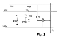
- 各画素が、フォトダイオード(PD)、電荷(ND)用の保存ノード、前記フォトダイオードから前記保存ノードへの電荷の転送を許す転送トランジスタ(T1)、前記保存ノード(T2)の電位をリセットするリセットトランジスタ、前記保存ノード内の電荷量を表す電位を生成するフォロワトランジスタ(T3)、および前記フォロワトランジスタを前記列導体に接続する行選択トランジスタ(T4)を含むことを特徴とする、請求項1〜6のいずれか1項に記載の画像センサ。
- 前記マトリクスの前記リセットトランジスタの全てを同時にオンにする共通リセット信号(RST)を発信する手段と、前記マトリクスの前記転送トランジスタの全てを同時にオンにする共通転送信号(GTRA)を発信する手段と、共通リセット命令の後、且つ共通転送命令の前に各行についてリセット電位のサンプリングを連続的に制御し、次いで前記転送命令の後で各行について有用電位のサンプリングを連続的に制御する手段とを含むことを特徴とする、請求項7に記載のセンサ。
Applications Claiming Priority (3)
| Application Number | Priority Date | Filing Date | Title |
|---|---|---|---|
| FR10/01911 | 2010-05-04 | ||
| FR1001911A FR2959901B1 (fr) | 2010-05-04 | 2010-05-04 | Capteur d'image a matrice d'echantillonneurs |
| PCT/EP2011/057152 WO2011138374A1 (fr) | 2010-05-04 | 2011-05-04 | Capteur d'image a matrice d'echantillonneurs |
Publications (2)
| Publication Number | Publication Date |
|---|---|
| JP2013529434A JP2013529434A (ja) | 2013-07-18 |
| JP5879655B2 true JP5879655B2 (ja) | 2016-03-08 |
Family
ID=43385156
Family Applications (1)
| Application Number | Title | Priority Date | Filing Date |
|---|---|---|---|
| JP2013508492A Expired - Fee Related JP5879655B2 (ja) | 2010-05-04 | 2011-05-04 | サンプラ配列を有する画像センサ |
Country Status (8)
| Country | Link |
|---|---|
| US (1) | US8982262B2 (ja) |
| EP (1) | EP2567541B1 (ja) |
| JP (1) | JP5879655B2 (ja) |
| KR (1) | KR20130069613A (ja) |
| CN (1) | CN102870407B (ja) |
| FR (1) | FR2959901B1 (ja) |
| IL (1) | IL222681A (ja) |
| WO (1) | WO2011138374A1 (ja) |
Families Citing this family (23)
| Publication number | Priority date | Publication date | Assignee | Title |
|---|---|---|---|---|
| US20060268360A1 (en) * | 2005-05-12 | 2006-11-30 | Jones Peter W J | Methods of creating a virtual window |
| US8564640B2 (en) * | 2007-11-16 | 2013-10-22 | Tenebraex Corporation | Systems and methods of creating a virtual window |
| US8791984B2 (en) * | 2007-11-16 | 2014-07-29 | Scallop Imaging, Llc | Digital security camera |
| WO2011037964A1 (en) * | 2009-09-22 | 2011-03-31 | Tenebraex Corporation | Systems and methods for correcting images in a multi-sensor system |
| JP5601001B2 (ja) * | 2010-03-31 | 2014-10-08 | ソニー株式会社 | 固体撮像素子および駆動方法、並びに電子機器 |
| US9049353B2 (en) | 2011-09-28 | 2015-06-02 | Semiconductor Components Industries, Llc | Time-delay-and-integrate image sensors having variable integration times |
| CN102801930B (zh) * | 2012-07-13 | 2014-05-14 | 天津大学 | 低功耗时间延时积分型 cmos 图像传感器 |
| US8975570B2 (en) | 2012-08-23 | 2015-03-10 | Teledyne Dalsa Inc. | CMOS time delay and integration image sensor |
| US9148601B2 (en) | 2012-09-26 | 2015-09-29 | Teledyne Dalsa, Inc. | CMOS TDI image sensor with rolling shutter pixels |
| US9973716B2 (en) | 2013-08-02 | 2018-05-15 | Samsung Electronics Co., Ltd. | Reset noise reduction for pixel readout with pseudo correlated double sampling |
| JP6331674B2 (ja) * | 2014-05-13 | 2018-05-30 | 株式会社リコー | 光電変換素子、画像読取装置及び画像形成装置 |
| US10075658B2 (en) * | 2014-05-30 | 2018-09-11 | Seek Thermal, Inc. | Data digitization and display for an imaging system |
| FR3024312B1 (fr) | 2014-07-28 | 2016-07-15 | E2V Semiconductors | Procede de capture d'image, a defilement et integration de signal, corrigeant des defauts d'image dus a des particules cosmiques |
| FR3024619B1 (fr) * | 2014-08-01 | 2016-07-29 | Pyxalis | Circuit integre photorepete avec compensation des retards de propagation de signaux, notamment de signaux d'horloge |
| KR102198853B1 (ko) | 2014-11-27 | 2021-01-05 | 삼성전자 주식회사 | 이미지 센서, 및 상기 이미지 센서를 포함하는 이미지 처리 시스템 |
| CN105741239B (zh) * | 2014-12-11 | 2018-11-30 | 合肥美亚光电技术股份有限公司 | 牙齿全景图像的生成方法、装置及用于拍摄牙齿的全景机 |
| FR3032105B1 (fr) * | 2015-01-30 | 2017-01-27 | E2V Semiconductors | Capteur radiologique avec detection de rayons x |
| CN112738365B (zh) * | 2015-07-16 | 2022-11-18 | 索尼公司 | 成像设备和信息处理系统 |
| CN108270942B (zh) * | 2018-01-31 | 2020-09-25 | 威海华菱光电股份有限公司 | 图像扫描装置、控制图像扫描光信号的接收方法及装置 |
| CN111314635B (zh) * | 2020-03-17 | 2022-07-26 | 合肥富煌君达高科信息技术有限公司 | 一种高速cmos图像传感器电路 |
| CN112019777B (zh) * | 2020-09-16 | 2021-10-26 | 南京大学 | 基于时间延迟积分(tdi)的图像传感器及其成像方法 |
| TWI795034B (zh) * | 2021-10-15 | 2023-03-01 | 原相科技股份有限公司 | 處置壞點的時延積分感測器 |
| JP2024013764A (ja) * | 2022-07-21 | 2024-02-01 | 日本電気株式会社 | 撮像装置、電子回路、撮像方法、プログラム |
Family Cites Families (7)
| Publication number | Priority date | Publication date | Assignee | Title |
|---|---|---|---|---|
| US6535247B1 (en) * | 1998-05-19 | 2003-03-18 | Pictos Technologies, Inc. | Active pixel sensor with capacitorless correlated double sampling |
| WO2001026382A1 (en) * | 1999-10-05 | 2001-04-12 | California Institute Of Technology | Time-delayed-integration imaging with active pixel sensors |
| US7009163B2 (en) * | 2001-06-22 | 2006-03-07 | Orbotech Ltd. | High-sensitivity optical scanning using memory integration |
| FR2906080B1 (fr) * | 2006-09-19 | 2008-11-28 | E2V Semiconductors Soc Par Act | Capteur d'image en defilement par integrations successives et sommation, a pixels cmos actifs |
| US7675561B2 (en) * | 2006-09-28 | 2010-03-09 | Cypress Semiconductor Corporation | Time delayed integration CMOS image sensor with zero desynchronization |
| GB0806427D0 (en) * | 2008-04-09 | 2008-05-14 | Cmosis Nv | Parallel analog-to-digital conversion in pixel arrays |
| JP4764905B2 (ja) * | 2008-08-11 | 2011-09-07 | キヤノン株式会社 | 撮像システム |
-
2010
- 2010-05-04 FR FR1001911A patent/FR2959901B1/fr not_active Expired - Fee Related
-
2011
- 2011-05-04 US US13/696,242 patent/US8982262B2/en not_active Expired - Fee Related
- 2011-05-04 JP JP2013508492A patent/JP5879655B2/ja not_active Expired - Fee Related
- 2011-05-04 CN CN201180022225.1A patent/CN102870407B/zh not_active Expired - Fee Related
- 2011-05-04 KR KR1020127028854A patent/KR20130069613A/ko not_active Ceased
- 2011-05-04 EP EP11718716.1A patent/EP2567541B1/fr active Active
- 2011-05-04 WO PCT/EP2011/057152 patent/WO2011138374A1/fr not_active Ceased
-
2012
- 2012-10-25 IL IL222681A patent/IL222681A/en active IP Right Grant
Also Published As
| Publication number | Publication date |
|---|---|
| US8982262B2 (en) | 2015-03-17 |
| KR20130069613A (ko) | 2013-06-26 |
| EP2567541A1 (fr) | 2013-03-13 |
| IL222681A (en) | 2017-02-28 |
| FR2959901B1 (fr) | 2015-07-24 |
| US20130050553A1 (en) | 2013-02-28 |
| FR2959901A1 (fr) | 2011-11-11 |
| JP2013529434A (ja) | 2013-07-18 |
| CN102870407A (zh) | 2013-01-09 |
| WO2011138374A1 (fr) | 2011-11-10 |
| IL222681A0 (en) | 2012-12-31 |
| EP2567541B1 (fr) | 2019-12-25 |
| CN102870407B (zh) | 2017-03-01 |
Similar Documents
| Publication | Publication Date | Title |
|---|---|---|
| JP5879655B2 (ja) | サンプラ配列を有する画像センサ | |
| JP5796261B2 (ja) | アナログおよびデジタル総和機能を備えたスワイプ式線形画像センサおよび対応する方法 | |
| JP5515172B2 (ja) | アクティブcmos画素を有し連続的に積分および合算を行う移動型画像センサ | |
| US11258977B2 (en) | Image sensor readout method and architecture | |
| JP6278730B2 (ja) | 固体撮像装置および撮像システム | |
| EP1233613B1 (en) | Active pixel image sensor with high dynamic range | |
| US7319423B2 (en) | Multi-mode ADC and its application to CMOS image sensors | |
| JP2001111900A (ja) | 固体撮像装置 | |
| TW200939758A (en) | Solid-state image sensing device, method for reading signal of solid-state image sensing device, and image pickup apparatus | |
| EP2560372B1 (en) | Solid-state imaging device | |
| US20140267884A1 (en) | Increasing Dynamic Range Using Multisampling | |
| CN108605105B (zh) | 固体摄像装置以及摄像装置 | |
| US9253426B2 (en) | Moving image sensor having multiphase digital summation and charge storage nodes separated from photodiodes by charge transfer gates | |
| KR20090128596A (ko) | 아날로그-디지털 변환 장치와 그 방법, 및 이미지 촬상장치 | |
| US8040417B2 (en) | Imaging element suitable for readout charges in plural times in a time dividing manner in one horizontal scanning period | |
| JP2010504009A (ja) | 電荷移動により動作するcmos線形画像センサ | |
| WO2017212075A2 (en) | Cmos image sensors with reduced power consumption | |
| US9531974B2 (en) | Two-line, shared pixel linear image sensor | |
| KR20120122165A (ko) | 광역 동적범위를 가지는 이미지 센서, 그 화소 회로 및 구동 방법 | |
| CN106454156A (zh) | 图像传感器及其运作方法 | |
| EP2560371B1 (en) | Solid-state imaging device | |
| JP5906596B2 (ja) | 撮像装置 | |
| JP2022065633A (ja) | 撮像装置、および画像センサの読み出し方法 | |
| JP2020028117A (ja) | 固体撮像素子 | |
| Huang et al. | Cmos image sensor binning circuit for low-light imaging |
Legal Events
| Date | Code | Title | Description |
|---|---|---|---|
| A621 | Written request for application examination |
Free format text: JAPANESE INTERMEDIATE CODE: A621 Effective date: 20140501 |
|
| A521 | Request for written amendment filed |
Free format text: JAPANESE INTERMEDIATE CODE: A523 Effective date: 20140703 |
|
| A131 | Notification of reasons for refusal |
Free format text: JAPANESE INTERMEDIATE CODE: A131 Effective date: 20150428 |
|
| A521 | Request for written amendment filed |
Free format text: JAPANESE INTERMEDIATE CODE: A523 Effective date: 20150724 |
|
| TRDD | Decision of grant or rejection written | ||
| A01 | Written decision to grant a patent or to grant a registration (utility model) |
Free format text: JAPANESE INTERMEDIATE CODE: A01 Effective date: 20151020 |
|
| A61 | First payment of annual fees (during grant procedure) |
Free format text: JAPANESE INTERMEDIATE CODE: A61 Effective date: 20151110 |
|
| A61 | First payment of annual fees (during grant procedure) |
Free format text: JAPANESE INTERMEDIATE CODE: A61 Effective date: 20160114 |
|
| R150 | Certificate of patent or registration of utility model |
Ref document number: 5879655 Country of ref document: JP Free format text: JAPANESE INTERMEDIATE CODE: R150 |
|
| S533 | Written request for registration of change of name |
Free format text: JAPANESE INTERMEDIATE CODE: R313533 |
|
| R350 | Written notification of registration of transfer |
Free format text: JAPANESE INTERMEDIATE CODE: R350 |
|
| R250 | Receipt of annual fees |
Free format text: JAPANESE INTERMEDIATE CODE: R250 |
|
| R250 | Receipt of annual fees |
Free format text: JAPANESE INTERMEDIATE CODE: R250 |
|
| R250 | Receipt of annual fees |
Free format text: JAPANESE INTERMEDIATE CODE: R250 |
|
| LAPS | Cancellation because of no payment of annual fees |