JP5906571B2 - 液晶表示装置、液晶表示装置の製造方法 - Google Patents
液晶表示装置、液晶表示装置の製造方法 Download PDFInfo
- Publication number
- JP5906571B2 JP5906571B2 JP2011038640A JP2011038640A JP5906571B2 JP 5906571 B2 JP5906571 B2 JP 5906571B2 JP 2011038640 A JP2011038640 A JP 2011038640A JP 2011038640 A JP2011038640 A JP 2011038640A JP 5906571 B2 JP5906571 B2 JP 5906571B2
- Authority
- JP
- Japan
- Prior art keywords
- liquid crystal
- convex
- concavo
- pixel electrode
- crystal layer
- Prior art date
- Legal status (The legal status is an assumption and is not a legal conclusion. Google has not performed a legal analysis and makes no representation as to the accuracy of the status listed.)
- Expired - Fee Related
Links
Images









Classifications
-
- G—PHYSICS
- G02—OPTICS
- G02F—OPTICAL DEVICES OR ARRANGEMENTS FOR THE CONTROL OF LIGHT BY MODIFICATION OF THE OPTICAL PROPERTIES OF THE MEDIA OF THE ELEMENTS INVOLVED THEREIN; NON-LINEAR OPTICS; FREQUENCY-CHANGING OF LIGHT; OPTICAL LOGIC ELEMENTS; OPTICAL ANALOGUE/DIGITAL CONVERTERS
- G02F1/00—Devices or arrangements for the control of the intensity, colour, phase, polarisation or direction of light arriving from an independent light source, e.g. switching, gating or modulating; Non-linear optics
- G02F1/01—Devices or arrangements for the control of the intensity, colour, phase, polarisation or direction of light arriving from an independent light source, e.g. switching, gating or modulating; Non-linear optics for the control of the intensity, phase, polarisation or colour
- G02F1/13—Devices or arrangements for the control of the intensity, colour, phase, polarisation or direction of light arriving from an independent light source, e.g. switching, gating or modulating; Non-linear optics for the control of the intensity, phase, polarisation or colour based on liquid crystals, e.g. single liquid crystal display cells
- G02F1/133—Constructional arrangements; Operation of liquid crystal cells; Circuit arrangements
- G02F1/1333—Constructional arrangements; Manufacturing methods
- G02F1/1337—Surface-induced orientation of the liquid crystal molecules, e.g. by alignment layers
- G02F1/133707—Structures for producing distorted electric fields, e.g. bumps, protrusions, recesses, slits in pixel electrodes
-
- G—PHYSICS
- G02—OPTICS
- G02F—OPTICAL DEVICES OR ARRANGEMENTS FOR THE CONTROL OF LIGHT BY MODIFICATION OF THE OPTICAL PROPERTIES OF THE MEDIA OF THE ELEMENTS INVOLVED THEREIN; NON-LINEAR OPTICS; FREQUENCY-CHANGING OF LIGHT; OPTICAL LOGIC ELEMENTS; OPTICAL ANALOGUE/DIGITAL CONVERTERS
- G02F1/00—Devices or arrangements for the control of the intensity, colour, phase, polarisation or direction of light arriving from an independent light source, e.g. switching, gating or modulating; Non-linear optics
- G02F1/01—Devices or arrangements for the control of the intensity, colour, phase, polarisation or direction of light arriving from an independent light source, e.g. switching, gating or modulating; Non-linear optics for the control of the intensity, phase, polarisation or colour
- G02F1/13—Devices or arrangements for the control of the intensity, colour, phase, polarisation or direction of light arriving from an independent light source, e.g. switching, gating or modulating; Non-linear optics for the control of the intensity, phase, polarisation or colour based on liquid crystals, e.g. single liquid crystal display cells
- G02F1/133—Constructional arrangements; Operation of liquid crystal cells; Circuit arrangements
- G02F1/1333—Constructional arrangements; Manufacturing methods
- G02F1/133371—Cells with varying thickness of the liquid crystal layer
-
- G—PHYSICS
- G02—OPTICS
- G02F—OPTICAL DEVICES OR ARRANGEMENTS FOR THE CONTROL OF LIGHT BY MODIFICATION OF THE OPTICAL PROPERTIES OF THE MEDIA OF THE ELEMENTS INVOLVED THEREIN; NON-LINEAR OPTICS; FREQUENCY-CHANGING OF LIGHT; OPTICAL LOGIC ELEMENTS; OPTICAL ANALOGUE/DIGITAL CONVERTERS
- G02F1/00—Devices or arrangements for the control of the intensity, colour, phase, polarisation or direction of light arriving from an independent light source, e.g. switching, gating or modulating; Non-linear optics
- G02F1/01—Devices or arrangements for the control of the intensity, colour, phase, polarisation or direction of light arriving from an independent light source, e.g. switching, gating or modulating; Non-linear optics for the control of the intensity, phase, polarisation or colour
- G02F1/13—Devices or arrangements for the control of the intensity, colour, phase, polarisation or direction of light arriving from an independent light source, e.g. switching, gating or modulating; Non-linear optics for the control of the intensity, phase, polarisation or colour based on liquid crystals, e.g. single liquid crystal display cells
- G02F1/133—Constructional arrangements; Operation of liquid crystal cells; Circuit arrangements
- G02F1/1333—Constructional arrangements; Manufacturing methods
- G02F1/1337—Surface-induced orientation of the liquid crystal molecules, e.g. by alignment layers
- G02F1/13378—Surface-induced orientation of the liquid crystal molecules, e.g. by alignment layers by treatment of the surface, e.g. embossing, rubbing or light irradiation
- G02F1/133788—Surface-induced orientation of the liquid crystal molecules, e.g. by alignment layers by treatment of the surface, e.g. embossing, rubbing or light irradiation by light irradiation, e.g. linearly polarised light photo-polymerisation
-
- G—PHYSICS
- G02—OPTICS
- G02F—OPTICAL DEVICES OR ARRANGEMENTS FOR THE CONTROL OF LIGHT BY MODIFICATION OF THE OPTICAL PROPERTIES OF THE MEDIA OF THE ELEMENTS INVOLVED THEREIN; NON-LINEAR OPTICS; FREQUENCY-CHANGING OF LIGHT; OPTICAL LOGIC ELEMENTS; OPTICAL ANALOGUE/DIGITAL CONVERTERS
- G02F1/00—Devices or arrangements for the control of the intensity, colour, phase, polarisation or direction of light arriving from an independent light source, e.g. switching, gating or modulating; Non-linear optics
- G02F1/01—Devices or arrangements for the control of the intensity, colour, phase, polarisation or direction of light arriving from an independent light source, e.g. switching, gating or modulating; Non-linear optics for the control of the intensity, phase, polarisation or colour
- G02F1/13—Devices or arrangements for the control of the intensity, colour, phase, polarisation or direction of light arriving from an independent light source, e.g. switching, gating or modulating; Non-linear optics for the control of the intensity, phase, polarisation or colour based on liquid crystals, e.g. single liquid crystal display cells
- G02F1/133—Constructional arrangements; Operation of liquid crystal cells; Circuit arrangements
- G02F1/1333—Constructional arrangements; Manufacturing methods
- G02F1/1339—Gaskets; Spacers; Sealing of cells
-
- G—PHYSICS
- G02—OPTICS
- G02F—OPTICAL DEVICES OR ARRANGEMENTS FOR THE CONTROL OF LIGHT BY MODIFICATION OF THE OPTICAL PROPERTIES OF THE MEDIA OF THE ELEMENTS INVOLVED THEREIN; NON-LINEAR OPTICS; FREQUENCY-CHANGING OF LIGHT; OPTICAL LOGIC ELEMENTS; OPTICAL ANALOGUE/DIGITAL CONVERTERS
- G02F1/00—Devices or arrangements for the control of the intensity, colour, phase, polarisation or direction of light arriving from an independent light source, e.g. switching, gating or modulating; Non-linear optics
- G02F1/01—Devices or arrangements for the control of the intensity, colour, phase, polarisation or direction of light arriving from an independent light source, e.g. switching, gating or modulating; Non-linear optics for the control of the intensity, phase, polarisation or colour
- G02F1/13—Devices or arrangements for the control of the intensity, colour, phase, polarisation or direction of light arriving from an independent light source, e.g. switching, gating or modulating; Non-linear optics for the control of the intensity, phase, polarisation or colour based on liquid crystals, e.g. single liquid crystal display cells
- G02F1/133—Constructional arrangements; Operation of liquid crystal cells; Circuit arrangements
- G02F1/1333—Constructional arrangements; Manufacturing methods
- G02F1/1343—Electrodes
- G02F1/13439—Electrodes characterised by their electrical, optical, physical properties; materials therefor; method of making
-
- G—PHYSICS
- G02—OPTICS
- G02F—OPTICAL DEVICES OR ARRANGEMENTS FOR THE CONTROL OF LIGHT BY MODIFICATION OF THE OPTICAL PROPERTIES OF THE MEDIA OF THE ELEMENTS INVOLVED THEREIN; NON-LINEAR OPTICS; FREQUENCY-CHANGING OF LIGHT; OPTICAL LOGIC ELEMENTS; OPTICAL ANALOGUE/DIGITAL CONVERTERS
- G02F1/00—Devices or arrangements for the control of the intensity, colour, phase, polarisation or direction of light arriving from an independent light source, e.g. switching, gating or modulating; Non-linear optics
- G02F1/01—Devices or arrangements for the control of the intensity, colour, phase, polarisation or direction of light arriving from an independent light source, e.g. switching, gating or modulating; Non-linear optics for the control of the intensity, phase, polarisation or colour
- G02F1/13—Devices or arrangements for the control of the intensity, colour, phase, polarisation or direction of light arriving from an independent light source, e.g. switching, gating or modulating; Non-linear optics for the control of the intensity, phase, polarisation or colour based on liquid crystals, e.g. single liquid crystal display cells
- G02F1/133—Constructional arrangements; Operation of liquid crystal cells; Circuit arrangements
- G02F1/1333—Constructional arrangements; Manufacturing methods
- G02F1/133357—Planarisation layers
-
- G—PHYSICS
- G02—OPTICS
- G02F—OPTICAL DEVICES OR ARRANGEMENTS FOR THE CONTROL OF LIGHT BY MODIFICATION OF THE OPTICAL PROPERTIES OF THE MEDIA OF THE ELEMENTS INVOLVED THEREIN; NON-LINEAR OPTICS; FREQUENCY-CHANGING OF LIGHT; OPTICAL LOGIC ELEMENTS; OPTICAL ANALOGUE/DIGITAL CONVERTERS
- G02F1/00—Devices or arrangements for the control of the intensity, colour, phase, polarisation or direction of light arriving from an independent light source, e.g. switching, gating or modulating; Non-linear optics
- G02F1/01—Devices or arrangements for the control of the intensity, colour, phase, polarisation or direction of light arriving from an independent light source, e.g. switching, gating or modulating; Non-linear optics for the control of the intensity, phase, polarisation or colour
- G02F1/13—Devices or arrangements for the control of the intensity, colour, phase, polarisation or direction of light arriving from an independent light source, e.g. switching, gating or modulating; Non-linear optics for the control of the intensity, phase, polarisation or colour based on liquid crystals, e.g. single liquid crystal display cells
- G02F1/133—Constructional arrangements; Operation of liquid crystal cells; Circuit arrangements
- G02F1/1333—Constructional arrangements; Manufacturing methods
- G02F1/1343—Electrodes
- G02F1/134309—Electrodes characterised by their geometrical arrangement
Landscapes
- Physics & Mathematics (AREA)
- Nonlinear Science (AREA)
- Mathematical Physics (AREA)
- Chemical & Material Sciences (AREA)
- Crystallography & Structural Chemistry (AREA)
- General Physics & Mathematics (AREA)
- Optics & Photonics (AREA)
- Spectroscopy & Molecular Physics (AREA)
- Liquid Crystal (AREA)
Description
1.実施の形態(画素電極の表面に凹凸構造を設け、裏面を平坦とした例)
2.変形例1(画素電極の下地層(平坦化膜)に凹凸構造を設けた例)
3.変形例2(画素電極の凹凸構造を2段階プロセスで形成した例)
4.変形例3(画素電極の凹凸構造がテーパを有する例)
5.変形例4(画素電極の凹凸構造が逆テーパを有する例)
6.変形例5−1〜5−5(画素電極の下地層に凹凸構造を設ける場合の詳細構成例)
7.変形例6(画素電極端部の構造例)
8.実施例
・実施例1(凹凸構造の段差を変化させた場合の透過率の測定結果)
・実施例2(変形例3において上底の幅を変化させた場合の透過率の測定結果)
・実施例3(変形例3において段差を変化させた場合の透過率の測定結果)
[液晶表示装置1の構成]
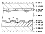
図1は、本発明の一実施の形態に係る液晶表示装置(液晶表示装置1)の全体構成を表すものである。液晶表示装置1は、例えば液晶表示パネル2、バックライト3、データドライバ51、ゲートドライバ52、タイミング制御部61およびバックライト駆動部62を備え、外部入力信号Dinに基づいて映像表示を行うものである。
画素電極13は、例えばITO(インジウム錫酸化物)やIZO等の透明導電膜からなり、表面(液晶層15側の面)に凹凸構造を有している。本実施の形態において、凹凸構造は、基板面に平行な方向に沿って交互に配列する凹面13aおよび凸面13bを有すると共に、これらの間の段差部分は、基板面に垂直な垂直面13cとなっている。尚、画素電極13の液晶層15側の面のみが凹凸構造を有しており、平坦化膜12側の面は平坦となっている。
尚、凹凸パターンとしては、このような凹面13aが4方向に沿って延在するパターンに限らず、例えばストライプ状やV字状など様々なパターンを採用できる。また、凹面13aの幅Sやその数、凸面13bの幅Lやその数についても任意に設定可能である。
(1.パネル封止工程)
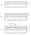
液晶表示装置1は、例えば次のようにして製造することができる。即ち、まず図8(A)に示したように、駆動基板11の表面を覆うように、平坦化膜12を例えばスピンコート法により成膜する。尚、この平坦化膜12の代わりに無機絶縁膜を成膜する場合には、例えばCVD法により、上述したようなシリコン酸化膜等を形成すればよい。この後、図8(B)に示したように、平坦化膜12上の全面に渡って、例えばITOよりなる画素電極13を例えば蒸着法やスパッタ法により成膜する。続いて、図8(C)に示したように、画素電極13の選択的な領域(凹面13aに対応する領域)を、例えばフォトリソグラフィによるハーフエッチング法により除去することにより、凹面13a,凸面13bおよび垂直面13cよりなる凹凸構造を形成する。尚、平坦化膜12にはコンタクトホールを設け、このコンタクトホールを介して画素電極13をそれぞれ、駆動基板11上に形成された駆動回路に電気的に接続されるようにする。
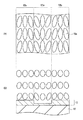
続いて、上記のようにして形成したパネル封止体において、液晶層15に電圧を印加しつつ露光(UV照射)することにより、液晶層15にプレチルトを付与する。具体的には、図9(A)に示したように、対向電極17および画素電極13を通じて液晶層15に電電圧Vを印加する。
(映像表示動作)
液晶表示装置1では、以下の要領で画素電極13と対向電極17との間に、外部入力信号Dinに基づく駆動電圧を印加することにより、映像が表示される。具体的には、タイミング制御部61の制御に応じて、ゲートドライバ52が、各画素10に接続されたゲート線に走査信号を順次供給すると共に、データドライバ51が、外部入力信号Dinに基づく映像信号を、所定のソース線に供給する。これにより、映像信号が供給されたソース線と走査信号が供給されたゲート線との交差点に位置する画素10が選択され、その画素10に駆動電圧が印加されることとなる。
図17は、変形例1に係る液晶表示装置における液晶表示パネルの断面構成(画素の一部に相当)を表すものである。本変形例の液晶表示パネルは、上記実施の形態の液晶表示パネル2と同様、駆動基板11と対向基板18との間に液晶層15を挟み込み、駆動基板11および対向基板18の外側に偏光板19,20が貼り合わせられたものである。また、駆動基板11上には、駆動基板11の表面を覆って平坦化膜21が形成され、この平坦化膜21上に、画素電極22が画素10毎に配設されている。このような構成において、本変形例においても、画素電極22の液晶層15側の面が凹凸構造を有し、対向電極17の液晶層15側の面は平坦となっている。
図19(A)〜(C)は、変形例2に係る液晶表示装置における画素電極13の他の製造方法を工程順に表したものである。上記実施の形態では、画素電極13の凹凸構造を、平坦化膜12上に画素電極13を全面形成した後、ハーフエッチングすることにより形成したが、次のようにして形成することも可能である。即ち、図19(A)に示したように、駆動基板11上に、平坦化膜21を形成した後、この平坦化膜21の全面に渡って、ITOよりなる電極層130を、例えば蒸着法やスパッタ法により成膜する。続いて、図19(B)に示したように、電極層130の選択的な領域(凹面13aに対応する領域)を、例えばフォトリソグラフィ法を用いたエッチングにより除去する。この後、図19(C)に示したように、ITOよりなる電極層131を、例えば蒸着法やスパッタ法により成膜する。これにより、露出した平坦化膜12の表面が電極層131によって覆われ、凹面13aおよび凸面13bを有する凹凸構造が形成される。
図20は、変形例3に係る液晶表示装置における液晶表示パネルの断面構成(画素の一部に相当)を表すものである。本変形例の液晶表示パネルは、上記実施の形態の液晶表示パネル2と同様、駆動基板11と対向基板18との間に液晶層15を挟み込み、駆動基板11および対向基板18の外側に偏光板19,20が貼り合わせられたものである。また、駆動基板11上には、平坦化膜12を介して画素電極23が画素10毎に配設されている。このような構成において、本変形例においても、画素電極23の液晶層15側の面が凹凸構造を有し、対向電極17の液晶層15側の面は平坦となっている。
図22は、変形例4に係る液晶表示装置における液晶表示パネルの断面構成(画素の一部に相当)を表すものである。本変形例の液晶表示パネルは、上記実施の形態の液晶表示パネル2と同様、駆動基板11と対向基板18との間に液晶層15を挟み込み、駆動基板11および対向基板18の外側に偏光板19,20が貼り合わせられたものである。また、駆動基板11上には、平坦化膜12を介して画素電極24が画素10毎に配設されている。このような構成において、本変形例においても、画素電極24の液晶層15側の面が凹凸構造を有し、対向電極17の液晶層15側の面は平坦となっている。
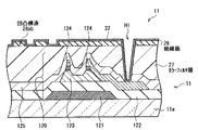
図23は、変形例5−1に係る凹凸構造例を説明するための断面図である。本変形例は、上記変形例1と同様の凹凸構造を有する場合(画素電極22の下地層である平坦化膜21の表面に凹凸構造21abを有する場合)の詳細構成例である。図23に示したように、平坦化膜21は、基板11a上のトランジスタ120(TFT)や図示しない配線等を覆うように設けられている。トランジスタ120は、例えばゲート電極121上に、ゲート絶縁膜122を介して半導体層123を有している。半導体層123上にはソース・ドレイン電極124が配設され、これらが保護膜125によって被覆されている。尚、トランジスタ120としては、そのようなボトムゲート型のものに限らず、トップゲート型のものであってもよい。
図24(A)は、変形例5−2に係る凹凸構造例を説明するための断面図である。本変形例は、上記変形例5−1と同様、画素電極22の下地層に凹凸構造を有するものであるが、次の点において上記変形例5−1と異なっている。即ち、本変形例では、平坦化膜12の表面が平坦となっており、この平坦化膜12上に凹凸構造25abを構成するフォトレジスト25が設けられている。平坦化膜12には、上記変形例5−1と同様、画素電極22とソース・ドレイン電極124との電気的導通を確保するためのコンタクトホールH1が設けられている。フォトレジスト25は、このコンタクトホールH1に対応する領域に開口を有すると共に、他の選択的な領域においてパターニングされて凹凸構造25abを形成している。画素電極22は、このフォトレジスト25上に、コンタクトホールH1の底部を埋め込むと共に、凹凸構造25abの形状に倣って、略一定の厚みで形成されている。
図25は、変形例5−3に係る凹凸構造例を説明するための断面図である。本変形例は、上記変形例5−1,5−2と同様、画素電極22の下地層に凹凸構造を有するものである。また、上記変形例5−2と同様、平坦化膜12の表面は平坦となっており、この平坦化膜12上に別途凹凸構造を形成するようになっている。但し、本変形例では、平坦化膜12上に、無機絶縁膜26が設けられ、この無機絶縁膜26に凹凸構造26abが形成されている。この無機絶縁膜26は、例えばシリコン酸化膜,シリコン窒化膜,シリコン酸窒化膜等により構成され、コンタクトホールH1に対応する領域と、凹凸構造26abを構成する領域とにおいてそれぞれパターニングされている。画素電極22は、この無機絶縁膜26上に、コンタクトホールH1の底部を埋め込むと共に、凹凸構造26abの形状に倣って、略一定の厚みで形成されている。
図26は、変形例5−4に係る凹凸構造例を説明するための断面図である。本変形例は、上記変形例5−1〜5−3と同様、画素電極22の下地層に凹凸構造を有するものである。但し、本変形例は、上記変形例5−1〜5−3と異なり、駆動基板11上にカラーフィルタ層27を有するCOA構造への適用例である。本変形例では、駆動基板11上に設けられたトランジスタ120を覆うようにカラーフィルタ層27が形成されている。このカラーフィルタ層27上には、このカラーフィルタ層27の保護層としての絶縁膜28が設けられており、この絶縁膜28が凹凸構造28abを有している。カラーフィルタ層27は、例えば樹脂材料と、顔料や染料等とを含むものであり、画素毎にR,G,Bのいずれかの色に塗り分けられている。絶縁膜28は、例えば熱硬化性樹脂、光反応性樹脂などの有機膜またはシリコン酸化膜、シリコン窒化膜、シリコン酸窒化膜などの無機膜により構成され、コンタクトホールH1に対応する領域と、凹凸構造28abを構成する領域とにおいてそれぞれパターニングされている。画素電極22は、この絶縁膜28上に、コンタクトホールH1の底部を埋め込むと共に、凹凸構造28abの形状に倣って、略一定の厚みで形成されている。
また、図27に示したように、上記変形例5−4で説明したようなCOA構造において、カラーフィルタ層29の表面に直に凹凸構造29abを形成してもよい。尚、この場合、上記変形例5−1において説明したような所定のフォトマスクを利用することで、凹凸構造29abを、コンタクトホールH1と同一工程において一括形成できる。また、本変形例では、カラーフィルタ層29の全面を画素電極22が覆い、この画素電極22がカラーフィルタ層29の保護膜として機能するようになっている。このように、カラーフィルタ層29自体に凹凸構造29abを設けてもよい。
図28(A),(B)は、画素電極端部の構成を説明するための模式図であり、(A)は斜視構成、(B)は駆動基板11上に平坦化膜21を介して設けられた画素電極22を画素電極22の側からみたものである。上記実施の形態および変形例において説明した画素電極では、その端部(具体的には、ブラクマトリクス層に対向する非表示部分)が除去されていてもよい。尚、画素電極としては、以下では、上記変形例1および変形例5−1〜5−5において説明した、凹凸構造を有する下地層の上に設けられた画素電極(画素電極22)を例に挙げる。具体的には、このような電極端22Eを有する画素電極22は、平坦化膜などの凹凸構造を有する下地層の上に画素電極22を形成した後、その端部をエッチング除去することにより形成する。
以下、上記実施の形態および変形例に係る液晶表示装置の実施例(実施例1〜3)について説明する。
図37に、上記実施の形態に係る液晶表示パネル2において、段差(凸面13bの厚みTbと凹面13aの厚みTaとの差)を変化させた場合の透過率の測定結果を示す。この際、ITOよりなる画素電極13の凹面13aの幅Sを4μm、凸面13bの幅Lを4μm、液晶層15の厚みを3.5μm、印加電圧を7.5V、入射光の波長を550nmとした。また、段差は、50nm〜500nmの範囲では50nm刻みで変化させ、1000nm〜3000nmの範囲では500nm刻みで変化させた。また、500nm〜800nmの範囲においては、750nmおよび800nmの2点において測定を行った。いずれの場合にも、液晶は問題なく配向したが、段差が大きくなるに従って、透過率は減少する傾向を示した。ここで、ファインスリット構造における透過率(REF=0.71)より高い透過率を実現できることから、段差は50nm〜750nmの範囲であることが望ましい。また、より望ましくは、50nm〜300nmである。成膜工程やエッチング工程におけるタクトタイムを短縮できると共に、段差が低減することにより、表面形状がフラットなベタ電極の構造により近づくため、透過率向上が期待できる。
実施例2として、上記変形例3で説明した画素電極23におけるテーパ面23cのテーパ角θtを変化させた場合の透過率を測定した。具体的には、図38に示したように、凹面23aの幅S(4μm),厚みTa(50nm),ピッチ(=台形状の凸部の下底の幅:4μm)および凸面23bの厚みTb(200nm)をそれぞれ固定とし、凸面23bの幅Daを可変として、テーパ角θtを変化させた。このとき、幅Daは、3.5〜1μmの範囲において0.5μm刻みで変化させた。いずれの場合にも、液晶は問題なく配向し、図39に示したように高透過率となった。また、透過率は、幅Daが1μmのときに最も高くなった。
実施例3として、上記実施例2と同様、テーパ面23cのテーパ角θtを変化させた場合の透過率を測定した。但し、本実施例では、図40に示したように、凹面23aの幅S(4μm),厚みTa(50nm),ピッチ(=台形状の凸部の下底の幅:4μm)および凸面23bの幅(1μm)をそれぞれ固定とし、凸面23bの厚みTbを可変として、段差(=Tb−50)を変化させた。段差は、200〜60nmの範囲において、20nm刻みで変化するようにした。いずれの場合にも、液晶は問題なく配向し、図41に示したように高透過率となった。また、段差が小さくなるに従ってより高い透過率を示した。
Claims (11)
- 垂直配向(VA:Vertical Alignment)型の液晶分子を含む液晶層と、
前記液晶層を挟んで対向配置された第1および第2の基板と、
前記第1の基板の前記液晶層側に設けられ、透明導電膜から構成された複数の画素電極と、
前記複数の画素電極に対向して、前記第2の基板に設けられた対向電極とを備え、
各画素電極では、前記液晶層側の面が凹凸構造を有すると共に、前記液晶層と反対側の面は、前記凹凸構造に対向する全域において連なった平坦面であり、
前記対向電極の前記液晶層側の面は平坦面であり、かつ
前記凹凸構造は、互いに異なる2以上の方向に沿って延在する複数の凹面を含むものである
液晶表示装置。 - 前記凹凸構造における凹面および凸面の外側端部が前記凹面および前記凸面の延在方向と直交する方向に沿って切断された形状を有する
請求項1に記載の液晶表示装置。 - 前記凹凸構造における凹面および凸面間の段差部分が基板面に垂直となっている
請求項1に記載の液晶表示装置。 - 前記凹凸構造における凹面および凸面間の段差部分がテーパ面である
請求項1に記載の液晶表示装置。 - 前記凹凸構造における凹面および凸面間の段差部分が逆テーパ面である
請求項1に記載の液晶表示装置。 - 前記液晶層では、前記画素電極および前記対向電極の近傍においてプレチルトが付与されている
請求項1に記載の液晶表示装置。 - 第1の基板上に、透明導電膜から構成された複数の画素電極を形成する工程と、
第2の基板上に対向電極を形成する工程と、
前記第1および第2の基板間に、前記画素電極および前記対向電極を対向させて、垂直配向(VA:Vertical Alignment)型の液晶分子を含む液晶層を封止する工程と、
前記画素電極と前記対向電極とを通じて前記液晶層に電圧を印加しつつ、前記液晶層を露光することにより、前記液晶層にプレチルトを付与する工程とを含み、
各画素電極では、前記液晶層側の面は凹凸構造を形成すると共に、前記液晶層と反対側の面は、前記凹凸構造に対向する全域において連なった平坦面であり、
前記対向電極では、前記液晶層側の面は平坦面であり、かつ
前記凹凸構造は、互いに異なる2以上の方向に沿って延在する複数の凹面を含むものである
液晶表示装置の製造方法。 - 前記凹凸構造における凹面および凸面の外側端部が前記凹面および前記凸面の延在方向と直交する方向に沿って切断された形状を有する
請求項7に記載の液晶表示装置の製造方法。 - 前記凹凸構造における凹面および凸面間の段差部分を基板面に垂直とする
請求項7に記載の液晶表示装置の製造方法。 - 前記凹凸構造における凹面および凸面間の段差部分をテーパ面とする
請求項7に記載の液晶表示装置の製造方法。 - 前記凹凸構造における凹面および凸面間の段差部分を逆テーパ面とする
請求項7に記載の液晶表示装置の製造方法。
Priority Applications (6)
| Application Number | Priority Date | Filing Date | Title |
|---|---|---|---|
| JP2011038640A JP5906571B2 (ja) | 2010-04-06 | 2011-02-24 | 液晶表示装置、液晶表示装置の製造方法 |
| US13/075,539 US9146422B2 (en) | 2010-04-06 | 2011-03-30 | Liquid crystal display and method of manufacturing liquid crystal display |
| KR1020110030999A KR101814208B1 (ko) | 2010-04-06 | 2011-04-05 | 액정 표시 장치, 액정 표시 장치의 제조 방법 |
| CN201110085988.2A CN102213874B (zh) | 2010-04-06 | 2011-04-06 | 液晶显示器及用于制造液晶显示器的方法 |
| TW100111890A TWI497177B (zh) | 2010-04-06 | 2011-04-06 | 液晶顯示器及其製造方法 |
| US14/671,404 US9507208B2 (en) | 2010-04-06 | 2015-03-27 | Liquid crystal display and method of manufacturing liquid crystal display |
Applications Claiming Priority (3)
| Application Number | Priority Date | Filing Date | Title |
|---|---|---|---|
| JP2010087658 | 2010-04-06 | ||
| JP2010087658 | 2010-04-06 | ||
| JP2011038640A JP5906571B2 (ja) | 2010-04-06 | 2011-02-24 | 液晶表示装置、液晶表示装置の製造方法 |
Publications (2)
| Publication Number | Publication Date |
|---|---|
| JP2011232736A JP2011232736A (ja) | 2011-11-17 |
| JP5906571B2 true JP5906571B2 (ja) | 2016-04-20 |
Family
ID=45322050
Family Applications (1)
| Application Number | Title | Priority Date | Filing Date |
|---|---|---|---|
| JP2011038640A Expired - Fee Related JP5906571B2 (ja) | 2010-04-06 | 2011-02-24 | 液晶表示装置、液晶表示装置の製造方法 |
Country Status (3)
| Country | Link |
|---|---|
| US (2) | US9146422B2 (ja) |
| JP (1) | JP5906571B2 (ja) |
| TW (1) | TWI497177B (ja) |
Families Citing this family (26)
| Publication number | Priority date | Publication date | Assignee | Title |
|---|---|---|---|---|
| US20120319277A1 (en) * | 2011-06-19 | 2012-12-20 | Shenzhen China Star Optoelectronics Technology, Co., Ltd. | Thin film transistor panel and manufacturing method thereof |
| JP6003192B2 (ja) * | 2012-04-27 | 2016-10-05 | ソニー株式会社 | 液晶表示装置 |
| US9057915B2 (en) * | 2012-05-29 | 2015-06-16 | International Business Machines Corporation | Liquid crystal integrated circuit and method to fabricate same |
| CN102723308B (zh) * | 2012-06-08 | 2014-09-24 | 京东方科技集团股份有限公司 | 一种阵列基板及其制作方法和显示装置 |
| JP2014081559A (ja) * | 2012-10-18 | 2014-05-08 | Sony Corp | 液晶表示装置 |
| JP2014095783A (ja) | 2012-11-08 | 2014-05-22 | Sony Corp | 液晶表示装置 |
| JP6194657B2 (ja) * | 2013-06-28 | 2017-09-13 | ソニー株式会社 | 液晶表示装置 |
| TWI512378B (zh) * | 2013-08-19 | 2015-12-11 | Au Optronics Corp | 畫素結構 |
| JP2015191232A (ja) | 2014-03-31 | 2015-11-02 | ソニー株式会社 | 液晶表示装置 |
| TWI564638B (zh) * | 2014-07-18 | 2017-01-01 | 友達光電股份有限公司 | 顯示面板之畫素結構 |
| US9577104B2 (en) | 2014-11-11 | 2017-02-21 | Shenzhen China Star Optoelectronics Technology Co., Ltd | COA substrate and liquid crystal display panel |
| CN104503155A (zh) * | 2014-11-17 | 2015-04-08 | 深圳市华星光电技术有限公司 | 液晶显示像素结构及其制作方法 |
| KR20160059580A (ko) | 2014-11-18 | 2016-05-27 | 삼성디스플레이 주식회사 | 액정 표시장치 및 이의 제조 방법 |
| US20160147093A1 (en) * | 2014-11-21 | 2016-05-26 | Shenzhen China Star Optoelectronics Technology Co., Ltd. | Display panel and display device |
| JP2016173544A (ja) | 2015-03-18 | 2016-09-29 | Jsr株式会社 | 液晶表示素子及びその製造方法、並びに液晶配向剤 |
| TWI525373B (zh) * | 2015-03-30 | 2016-03-11 | 友達光電股份有限公司 | 畫素結構以及顯示面板 |
| TWI564642B (zh) | 2015-08-21 | 2017-01-01 | 友達光電股份有限公司 | 液晶顯示面板其液晶配向方法 |
| TWI564616B (zh) | 2015-08-24 | 2017-01-01 | 友達光電股份有限公司 | 顯示面板 |
| KR102410039B1 (ko) * | 2015-11-30 | 2022-06-20 | 엘지디스플레이 주식회사 | 표시장치의 화소구조 및 이를 포함한 터치스크린 내장형 표시장치 |
| CN106932969B (zh) | 2015-12-29 | 2020-07-10 | 群创光电股份有限公司 | 显示器 |
| KR102502218B1 (ko) | 2016-04-08 | 2023-02-21 | 삼성디스플레이 주식회사 | 액정 표시 장치 및 액정 표시 장치 제조방법 |
| JP2018112700A (ja) * | 2017-01-13 | 2018-07-19 | 株式会社ジャパンディスプレイ | 表示装置及び電子棚札 |
| CN111785740B (zh) * | 2020-07-17 | 2025-04-29 | 武汉华星光电半导体显示技术有限公司 | 一种薄膜晶体管阵列基板及显示装置 |
| CN112068373B (zh) * | 2020-09-10 | 2022-05-03 | 深圳市华星光电半导体显示技术有限公司 | 阵列基板及其制作方法、显示面板 |
| US12025888B2 (en) * | 2021-08-19 | 2024-07-02 | Shenzhen China Star Optoelectronics Semiconductor Display Technology Co., Ltd. | Liquid crystal display panel, liquid crystal alignment method, and mobile terminal |
| CN117608130A (zh) * | 2023-11-10 | 2024-02-27 | 厦门天马光电子有限公司 | 一种显示面板及显示装置 |
Family Cites Families (25)
| Publication number | Priority date | Publication date | Assignee | Title |
|---|---|---|---|---|
| SG50586A1 (en) | 1991-07-26 | 2000-05-23 | Rolic Ag | Liquid crystal display cell |
| JPH0733612A (ja) | 1993-07-22 | 1995-02-03 | Ishihara Sangyo Kaisha Ltd | 安定化された油性懸濁状除草組成物 |
| JPH07333634A (ja) * | 1994-06-10 | 1995-12-22 | Sony Corp | 液晶表示パネル |
| JP3284292B2 (ja) * | 1994-06-10 | 2002-05-20 | 三菱電機株式会社 | 液晶表示装置 |
| US6504592B1 (en) * | 1999-06-16 | 2003-01-07 | Nec Corporation | Liquid crystal display and method of manufacturing the same and method of driving the same |
| JP3404467B2 (ja) * | 2000-02-24 | 2003-05-06 | シャープ株式会社 | 液晶表示装置 |
| JP3564417B2 (ja) * | 2000-05-31 | 2004-09-08 | Nec液晶テクノロジー株式会社 | カラー液晶表示装置及びその製造方法 |
| US6977704B2 (en) | 2001-03-30 | 2005-12-20 | Fujitsu Display Technologies Corporation | Liquid crystal display |
| JP2003066455A (ja) * | 2001-08-30 | 2003-03-05 | Toshiba Corp | 液晶表示装置、液晶表示装置の製造方法及びカラーフィルタ基板 |
| US7113241B2 (en) * | 2001-08-31 | 2006-09-26 | Sharp Kabushiki Kaisha | Liquid crystal display and method of manufacturing the same |
| JP2003075839A (ja) * | 2001-09-07 | 2003-03-12 | Toshiba Corp | 液晶表示装置 |
| JP4237977B2 (ja) * | 2001-10-02 | 2009-03-11 | シャープ株式会社 | 液晶表示装置 |
| JP2003241222A (ja) * | 2002-02-15 | 2003-08-27 | Matsushita Electric Ind Co Ltd | 反射型液晶表示装置 |
| KR100720450B1 (ko) * | 2002-12-23 | 2007-05-22 | 엘지.필립스 엘시디 주식회사 | 멀티도메인 액정표시장치 및 그 제조방법 |
| JP4364542B2 (ja) * | 2003-03-31 | 2009-11-18 | シャープ株式会社 | 液晶表示装置およびその製造方法 |
| TW200528831A (en) * | 2004-01-06 | 2005-09-01 | Samsung Electronics Co Ltd | Substrate for a display apparatus |
| JP2005316330A (ja) * | 2004-04-30 | 2005-11-10 | Toshiba Matsushita Display Technology Co Ltd | 液晶表示装置 |
| US20050270462A1 (en) * | 2004-05-21 | 2005-12-08 | Norio Koma | Liquid crystal display device |
| JP4638280B2 (ja) | 2005-05-25 | 2011-02-23 | 株式会社 日立ディスプレイズ | 液晶表示装置 |
| TWI338172B (en) * | 2005-12-30 | 2011-03-01 | Au Optronics Corp | Method of forming spacers and alignment protrusions simultaneously on color filter substrate |
| JP4766037B2 (ja) * | 2007-11-27 | 2011-09-07 | セイコーエプソン株式会社 | 液晶表示装置、電子機器 |
| KR20090059957A (ko) * | 2007-12-07 | 2009-06-11 | 삼성전자주식회사 | 액정 표시 장치 |
| TWI384275B (zh) * | 2008-05-30 | 2013-02-01 | Chimei Innolux Corp | 液晶顯示面板 |
| TW201003258A (en) * | 2008-07-08 | 2010-01-16 | Chi Mei Optoelectronics Corp | Liquid crystal display and pixel structure |
| KR20100065876A (ko) * | 2008-12-09 | 2010-06-17 | 삼성전자주식회사 | 액정 표시 장치 및 이의 제조 방법 |
-
2011
- 2011-02-24 JP JP2011038640A patent/JP5906571B2/ja not_active Expired - Fee Related
- 2011-03-30 US US13/075,539 patent/US9146422B2/en active Active
- 2011-04-06 TW TW100111890A patent/TWI497177B/zh not_active IP Right Cessation
-
2015
- 2015-03-27 US US14/671,404 patent/US9507208B2/en not_active Expired - Fee Related
Also Published As
| Publication number | Publication date |
|---|---|
| TWI497177B (zh) | 2015-08-21 |
| US9507208B2 (en) | 2016-11-29 |
| US9146422B2 (en) | 2015-09-29 |
| JP2011232736A (ja) | 2011-11-17 |
| TW201142445A (en) | 2011-12-01 |
| US20150198836A1 (en) | 2015-07-16 |
| US20110317104A1 (en) | 2011-12-29 |
Similar Documents
| Publication | Publication Date | Title |
|---|---|---|
| JP5906571B2 (ja) | 液晶表示装置、液晶表示装置の製造方法 | |
| KR101814208B1 (ko) | 액정 표시 장치, 액정 표시 장치의 제조 방법 | |
| CN1301438C (zh) | 液晶显示装置和电子设备 | |
| TWI584032B (zh) | 液晶顯示裝置 | |
| US20100091234A1 (en) | Liquid Crystal Display Device | |
| US20050195353A1 (en) | Liquid crystal display apparatus and method of manufacturing the same | |
| US8451411B2 (en) | Display panel having a domain divider | |
| KR20090090817A (ko) | 액정 표시 장치의 제조 방법 | |
| US10082702B2 (en) | Liquid-crystal display apparatus and method of giving a pretilt to liquid-crystal molecules | |
| KR101380784B1 (ko) | 액정표시장치의 제조방법 | |
| KR101146985B1 (ko) | 표시 장치 및 이의 제조 방법 | |
| US20190369424A1 (en) | Liquid crystal display device | |
| JP2009186822A (ja) | 液晶表示パネル及び液晶表示パネルの製造方法 | |
| KR20040060107A (ko) | 횡전계 방식의 액정표시장치 | |
| KR100840095B1 (ko) | 액정표시장치 및 그 제조방법 | |
| US20070153213A1 (en) | Method of forming spacers and alignment protrusions simultaneously | |
| US20090279036A1 (en) | Display substrate, a method of manufacturing the same and a display apparatus having the same | |
| US7812908B2 (en) | Display apparatus and method for manufacturing substrate for display apparatus | |
| KR100484948B1 (ko) | 횡전계 방식의 액정표시장치 | |
| JP2004206080A (ja) | 液晶表示装置および電子機器 | |
| KR101068354B1 (ko) | 액정표시장치 및 그 제조방법 | |
| KR20040062212A (ko) | 액정표시장치 | |
| CN108415113A (zh) | 偏振片、偏振片的制作方法及显示装置 | |
| KR20060006529A (ko) | 액정표시장치와 그 제조방법 | |
| KR20070002711A (ko) | 반사-투과형 액정표시장치의 제조방법 |
Legal Events
| Date | Code | Title | Description |
|---|---|---|---|
| A621 | Written request for application examination |
Free format text: JAPANESE INTERMEDIATE CODE: A621 Effective date: 20140204 |
|
| A131 | Notification of reasons for refusal |
Free format text: JAPANESE INTERMEDIATE CODE: A131 Effective date: 20140924 |
|
| A977 | Report on retrieval |
Free format text: JAPANESE INTERMEDIATE CODE: A971007 Effective date: 20140924 |
|
| A521 | Request for written amendment filed |
Free format text: JAPANESE INTERMEDIATE CODE: A523 Effective date: 20141112 |
|
| A131 | Notification of reasons for refusal |
Free format text: JAPANESE INTERMEDIATE CODE: A131 Effective date: 20150421 |
|
| A521 | Request for written amendment filed |
Free format text: JAPANESE INTERMEDIATE CODE: A523 Effective date: 20150615 |
|
| A131 | Notification of reasons for refusal |
Free format text: JAPANESE INTERMEDIATE CODE: A131 Effective date: 20151104 |
|
| A521 | Request for written amendment filed |
Free format text: JAPANESE INTERMEDIATE CODE: A523 Effective date: 20151215 |
|
| TRDD | Decision of grant or rejection written | ||
| A01 | Written decision to grant a patent or to grant a registration (utility model) |
Free format text: JAPANESE INTERMEDIATE CODE: A01 Effective date: 20160223 |
|
| A61 | First payment of annual fees (during grant procedure) |
Free format text: JAPANESE INTERMEDIATE CODE: A61 Effective date: 20160307 |
|
| R151 | Written notification of patent or utility model registration |
Ref document number: 5906571 Country of ref document: JP Free format text: JAPANESE INTERMEDIATE CODE: R151 |
|
| R250 | Receipt of annual fees |
Free format text: JAPANESE INTERMEDIATE CODE: R250 |
|
| R250 | Receipt of annual fees |
Free format text: JAPANESE INTERMEDIATE CODE: R250 |
|
| LAPS | Cancellation because of no payment of annual fees |