JP5940775B2 - 液晶表示装置バックライト用led光源装置および液晶表示装置 - Google Patents
液晶表示装置バックライト用led光源装置および液晶表示装置 Download PDFInfo
- Publication number
- JP5940775B2 JP5940775B2 JP2011166236A JP2011166236A JP5940775B2 JP 5940775 B2 JP5940775 B2 JP 5940775B2 JP 2011166236 A JP2011166236 A JP 2011166236A JP 2011166236 A JP2011166236 A JP 2011166236A JP 5940775 B2 JP5940775 B2 JP 5940775B2
- Authority
- JP
- Japan
- Prior art keywords
- light source
- source device
- led light
- liquid crystal
- substrate
- Prior art date
- Legal status (The legal status is an assumption and is not a legal conclusion. Google has not performed a legal analysis and makes no representation as to the accuracy of the status listed.)
- Expired - Fee Related
Links
Images


















Classifications
-
- H—ELECTRICITY
- H05—ELECTRIC TECHNIQUES NOT OTHERWISE PROVIDED FOR
- H05K—PRINTED CIRCUITS; CASINGS OR CONSTRUCTIONAL DETAILS OF ELECTRIC APPARATUS; MANUFACTURE OF ASSEMBLAGES OF ELECTRICAL COMPONENTS
- H05K1/00—Printed circuits
- H05K1/02—Details
- H05K1/03—Use of materials for the substrate
- H05K1/0306—Inorganic insulating substrates, e.g. ceramic, glass
-
- G—PHYSICS
- G02—OPTICS
- G02B—OPTICAL ELEMENTS, SYSTEMS OR APPARATUS
- G02B6/00—Light guides; Structural details of arrangements comprising light guides and other optical elements, e.g. couplings
- G02B6/0001—Light guides; Structural details of arrangements comprising light guides and other optical elements, e.g. couplings specially adapted for lighting devices or systems
- G02B6/0011—Light guides; Structural details of arrangements comprising light guides and other optical elements, e.g. couplings specially adapted for lighting devices or systems the light guides being planar or of plate-like form
- G02B6/0066—Light guides; Structural details of arrangements comprising light guides and other optical elements, e.g. couplings specially adapted for lighting devices or systems the light guides being planar or of plate-like form characterised by the light source being coupled to the light guide
- G02B6/0073—Light emitting diode [LED]
-
- G—PHYSICS
- G02—OPTICS
- G02B—OPTICAL ELEMENTS, SYSTEMS OR APPARATUS
- G02B6/00—Light guides; Structural details of arrangements comprising light guides and other optical elements, e.g. couplings
- G02B6/0001—Light guides; Structural details of arrangements comprising light guides and other optical elements, e.g. couplings specially adapted for lighting devices or systems
- G02B6/0011—Light guides; Structural details of arrangements comprising light guides and other optical elements, e.g. couplings specially adapted for lighting devices or systems the light guides being planar or of plate-like form
- G02B6/0013—Means for improving the coupling-in of light from the light source into the light guide
- G02B6/0023—Means for improving the coupling-in of light from the light source into the light guide provided by one optical element, or plurality thereof, placed between the light guide and the light source, or around the light source
- G02B6/0031—Reflecting element, sheet or layer
-
- G—PHYSICS
- G02—OPTICS
- G02B—OPTICAL ELEMENTS, SYSTEMS OR APPARATUS
- G02B6/00—Light guides; Structural details of arrangements comprising light guides and other optical elements, e.g. couplings
- G02B6/0001—Light guides; Structural details of arrangements comprising light guides and other optical elements, e.g. couplings specially adapted for lighting devices or systems
- G02B6/0011—Light guides; Structural details of arrangements comprising light guides and other optical elements, e.g. couplings specially adapted for lighting devices or systems the light guides being planar or of plate-like form
- G02B6/0066—Light guides; Structural details of arrangements comprising light guides and other optical elements, e.g. couplings specially adapted for lighting devices or systems the light guides being planar or of plate-like form characterised by the light source being coupled to the light guide
- G02B6/0068—Arrangements of plural sources, e.g. multi-colour light sources
-
- G—PHYSICS
- G02—OPTICS
- G02B—OPTICAL ELEMENTS, SYSTEMS OR APPARATUS
- G02B6/00—Light guides; Structural details of arrangements comprising light guides and other optical elements, e.g. couplings
- G02B6/0001—Light guides; Structural details of arrangements comprising light guides and other optical elements, e.g. couplings specially adapted for lighting devices or systems
- G02B6/0011—Light guides; Structural details of arrangements comprising light guides and other optical elements, e.g. couplings specially adapted for lighting devices or systems the light guides being planar or of plate-like form
- G02B6/0081—Mechanical or electrical aspects of the light guide and light source in the lighting device peculiar to the adaptation to planar light guides, e.g. concerning packaging
- G02B6/0083—Details of electrical connections of light sources to drivers, circuit boards, or the like
-
- H—ELECTRICITY
- H05—ELECTRIC TECHNIQUES NOT OTHERWISE PROVIDED FOR
- H05K—PRINTED CIRCUITS; CASINGS OR CONSTRUCTIONAL DETAILS OF ELECTRIC APPARATUS; MANUFACTURE OF ASSEMBLAGES OF ELECTRICAL COMPONENTS
- H05K2201/00—Indexing scheme relating to printed circuits covered by H05K1/00
- H05K2201/01—Dielectrics
- H05K2201/0137—Materials
- H05K2201/017—Glass ceramic coating, e.g. formed on inorganic substrate
-
- H—ELECTRICITY
- H05—ELECTRIC TECHNIQUES NOT OTHERWISE PROVIDED FOR
- H05K—PRINTED CIRCUITS; CASINGS OR CONSTRUCTIONAL DETAILS OF ELECTRIC APPARATUS; MANUFACTURE OF ASSEMBLAGES OF ELECTRICAL COMPONENTS
- H05K2201/00—Indexing scheme relating to printed circuits covered by H05K1/00
- H05K2201/10—Details of components or other objects attached to or integrated in a printed circuit board
- H05K2201/10007—Types of components
- H05K2201/10106—Light emitting diode [LED]
-
- H—ELECTRICITY
- H05—ELECTRIC TECHNIQUES NOT OTHERWISE PROVIDED FOR
- H05K—PRINTED CIRCUITS; CASINGS OR CONSTRUCTIONAL DETAILS OF ELECTRIC APPARATUS; MANUFACTURE OF ASSEMBLAGES OF ELECTRICAL COMPONENTS
- H05K2201/00—Indexing scheme relating to printed circuits covered by H05K1/00
- H05K2201/20—Details of printed circuits not provided for in H05K2201/01 - H05K2201/10
- H05K2201/2054—Light-reflecting surface, e.g. conductors, substrates, coatings, dielectrics
-
- H—ELECTRICITY
- H10—SEMICONDUCTOR DEVICES; ELECTRIC SOLID-STATE DEVICES NOT OTHERWISE PROVIDED FOR
- H10H—INORGANIC LIGHT-EMITTING SEMICONDUCTOR DEVICES HAVING POTENTIAL BARRIERS
- H10H20/00—Individual inorganic light-emitting semiconductor devices having potential barriers, e.g. light-emitting diodes [LED]
- H10H20/80—Constructional details
- H10H20/85—Packages
- H10H20/855—Optical field-shaping means, e.g. lenses
- H10H20/856—Reflecting means
-
- H—ELECTRICITY
- H10—SEMICONDUCTOR DEVICES; ELECTRIC SOLID-STATE DEVICES NOT OTHERWISE PROVIDED FOR
- H10W—GENERIC PACKAGES, INTERCONNECTIONS, CONNECTORS OR OTHER CONSTRUCTIONAL DETAILS OF DEVICES COVERED BY CLASS H10
- H10W72/00—Interconnections or connectors in packages
- H10W72/071—Connecting or disconnecting
- H10W72/075—Connecting or disconnecting of bond wires
- H10W72/07551—Connecting or disconnecting of bond wires characterised by changes in properties of the bond wires during the connecting
- H10W72/07554—Connecting or disconnecting of bond wires characterised by changes in properties of the bond wires during the connecting changes in dispositions
-
- H—ELECTRICITY
- H10—SEMICONDUCTOR DEVICES; ELECTRIC SOLID-STATE DEVICES NOT OTHERWISE PROVIDED FOR
- H10W—GENERIC PACKAGES, INTERCONNECTIONS, CONNECTORS OR OTHER CONSTRUCTIONAL DETAILS OF DEVICES COVERED BY CLASS H10
- H10W72/00—Interconnections or connectors in packages
- H10W72/30—Die-attach connectors
-
- H—ELECTRICITY
- H10—SEMICONDUCTOR DEVICES; ELECTRIC SOLID-STATE DEVICES NOT OTHERWISE PROVIDED FOR
- H10W—GENERIC PACKAGES, INTERCONNECTIONS, CONNECTORS OR OTHER CONSTRUCTIONAL DETAILS OF DEVICES COVERED BY CLASS H10
- H10W72/00—Interconnections or connectors in packages
- H10W72/50—Bond wires
- H10W72/541—Dispositions of bond wires
- H10W72/547—Dispositions of multiple bond wires
-
- H—ELECTRICITY
- H10—SEMICONDUCTOR DEVICES; ELECTRIC SOLID-STATE DEVICES NOT OTHERWISE PROVIDED FOR
- H10W—GENERIC PACKAGES, INTERCONNECTIONS, CONNECTORS OR OTHER CONSTRUCTIONAL DETAILS OF DEVICES COVERED BY CLASS H10
- H10W72/00—Interconnections or connectors in packages
- H10W72/851—Dispositions of multiple connectors or interconnections
- H10W72/874—On different surfaces
- H10W72/884—Die-attach connectors and bond wires
-
- H—ELECTRICITY
- H10—SEMICONDUCTOR DEVICES; ELECTRIC SOLID-STATE DEVICES NOT OTHERWISE PROVIDED FOR
- H10W—GENERIC PACKAGES, INTERCONNECTIONS, CONNECTORS OR OTHER CONSTRUCTIONAL DETAILS OF DEVICES COVERED BY CLASS H10
- H10W90/00—Package configurations
- H10W90/701—Package configurations characterised by the relative positions of pads or connectors relative to package parts
- H10W90/751—Package configurations characterised by the relative positions of pads or connectors relative to package parts of bond wires
- H10W90/754—Package configurations characterised by the relative positions of pads or connectors relative to package parts of bond wires between a chip and a stacked insulating package substrate, interposer or RDL
Landscapes
- Engineering & Computer Science (AREA)
- Microelectronics & Electronic Packaging (AREA)
- Physics & Mathematics (AREA)
- Chemical & Material Sciences (AREA)
- Ceramic Engineering (AREA)
- Inorganic Chemistry (AREA)
- General Physics & Mathematics (AREA)
- Optics & Photonics (AREA)
- Liquid Crystal (AREA)
- Planar Illumination Modules (AREA)
- Led Device Packages (AREA)
Description
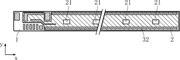
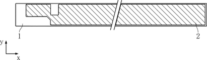
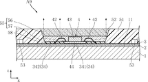
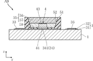
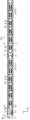
A1〜A14(液晶表示装置バックライト用)LED光源装置
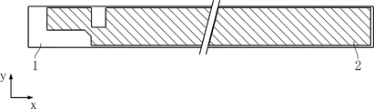
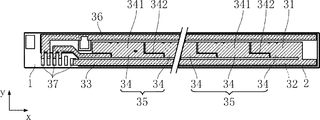
1 基板
11 主面
2 ガラス層
21 窓部
22 傾斜面
3 金属膜
31 Al層
32 AgPt層
33 共通帯状部
34 アイランド部
341 本体部
342 延出部
35 アイランド群
36 連絡帯状部
37 接続端子部
38 配線
4 LEDチップ
41 ツェナーダイオード
42 ワイヤ
43 半導体層
44 基板
441 スルーホール電極
442 バンプ
481 電極
51 リフレクタ
511 底面
512 突出部
52 開口
53 凹部
55 透光樹脂
56 蛍光部
57 透明部
58 白色樹脂(不透明樹脂)
591 (第1)表面
592,593 (第2)表面
594 (第3)表面
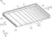
6 導光板
61 入射面
62 反射面
621 溝
63 出射面
7 液晶パネル
8 接着層
Claims (16)
- 複数のLEDチップを備える液晶表示装置バックライト用LED光源装置であって、
基板と、
上記基板の主面を覆う金属膜と、
上記金属膜と上記基板との間に介在するガラス層とを備えており、
上記複数のLEDチップは、上記金属膜に実装されており、
上記ガラス層には、上記基板の厚さ方向視において上記LEDチップを内包する窓部が設けられていることを特徴とする、液晶表示装置バックライト用LED光源装置。 - 上記ガラス層は、上記窓部の縁につながっており、かつ上記LEDチップから遠ざかるほど、上記基板の主面からその法線方向に遠ざかるように傾斜した傾斜面を有する、請求項1に記載の液晶表示装置バックライト用LED光源装置。
- 上記傾斜面は、上記LEDチップを囲む枠状である、請求項2に記載の液晶表示装置バックライト用LED光源装置。
- 上記基板は、セラミックスからなる、請求項1ないし3のいずれかに記載の液晶表示装置バックライト用LED光源装置。
- 上記金属膜は、少なくともその最外層がAl層からなる、請求項1ないし4のいずれかに記載の液晶表示装置バックライト用LED光源装置。
- 上記金属膜は、上記Al層の少なくとも一部と上記基板との間に介在するAgPt層をさらに含む、請求項5に記載の液晶表示装置バックライト用LED光源装置。
- 上記金属膜は、AgPt層のみからなる、請求項1ないし4のいずれかに記載の液晶表示装置バックライト用LED光源装置。
- 上記Al層は、スパッタ膜からなる、請求項5または6に記載の液晶表示装置バックライト用LED光源装置。
- 上記LEDチップを囲む枠状のリフレクタをさらに備えている、請求項1ないし8のいずれかに記載の液晶表示装置バックライト用LED光源装置。
- 上記リフレクタは、白色樹脂からなる、請求項9に記載の液晶表示装置バックライト用LED光源装置。
- 上記リフレクタが囲う空間には、上記LEDチップを覆う透光樹脂が充填されている、請求項9または10に記載の液晶表示装置バックライト用LED光源装置。
- 上記透光樹脂には、蛍光材料が混入されている、請求項11に記載の液晶表示装置バックライト用LED光源装置。
- 上記基板は、長矩形状であり、
上記複数のLEDチップは、上記基板の長手方向に沿って配列されている、請求項1ないし12のいずれかに記載の液晶表示装置バックライト用LED光源装置。 - 上記金属膜は、上記基板の幅方向一端寄りにおいて上記基板の長手方向に長く延びる共通帯状部と、上記共通帯状部と平行に配列されており、かつ上記長手方向において最も端に位置するものが上記共通帯状部と導通する複数のアイランド部からなる1以上のアイランド群と、を有しており、
上記複数のLEDチップは、上記複数のアイランド部に各別に実装されている、請求項13に記載の液晶表示装置バックライト用LED光源装置。 - 上記金属膜は、上記基板の長手方向一端寄りに設けられた接続端子部と、上記共通帯状部に沿って上記長手方向に配列された2つの上記アイランド群と、上記基板の幅方向において上記共通帯状部とは上記アイランド群を挟んで反対側に配置されており、上記長手方向に沿って上記接続端子部から長く延びており、かつ上記2つのアイランド群のうち上記接続端子部から遠いものに含まれる上記複数のアイランド部のうち上記接続端子部にもっとも近いものと導通する連絡帯状部と、を有する、請求項14に記載の液晶表示装置バックライト用LED光源装置。
- 請求項1ないし15のいずれかに記載の液晶表示装置バックライト用LED光源装置と、
全体略板状であり、厚さ方向に沿って広がるとともに上記液晶表示装置バックライト用LED光源装置と正対する入射面、上記厚さ方向と直角である方向に広がるとともに上記入射面から進行してきた光を上記厚さ方向に向けて反射する反射面、および上記反射面と上記厚さ方向において離間しているとともに上記反射面から進行してきた光を出射する出射面を有する導光部材と、
上記出射面から出射された光を選択的に透過させることにより画像を形成する液晶パネルと、
を備えることを特徴とする、液晶表示装置。
Priority Applications (3)
| Application Number | Priority Date | Filing Date | Title |
|---|---|---|---|
| JP2011166236A JP5940775B2 (ja) | 2010-08-27 | 2011-07-29 | 液晶表示装置バックライト用led光源装置および液晶表示装置 |
| US13/217,929 US9510442B2 (en) | 2010-08-27 | 2011-08-25 | LED light source unit for backlight of liquid crystal display, and liquid crystal display |
| CN201110253637.8A CN102384405B (zh) | 2010-08-27 | 2011-08-26 | 液晶显示装置背光源用led光源装置和液晶显示装置 |
Applications Claiming Priority (9)
| Application Number | Priority Date | Filing Date | Title |
|---|---|---|---|
| JP2010190469 | 2010-08-27 | ||
| JP2010190469 | 2010-08-27 | ||
| JP2010259269 | 2010-11-19 | ||
| JP2010259270 | 2010-11-19 | ||
| JP2010259270 | 2010-11-19 | ||
| JP2010259269 | 2010-11-19 | ||
| JP2011144716 | 2011-06-29 | ||
| JP2011144716 | 2011-06-29 | ||
| JP2011166236A JP5940775B2 (ja) | 2010-08-27 | 2011-07-29 | 液晶表示装置バックライト用led光源装置および液晶表示装置 |
Publications (2)
| Publication Number | Publication Date |
|---|---|
| JP2013033777A JP2013033777A (ja) | 2013-02-14 |
| JP5940775B2 true JP5940775B2 (ja) | 2016-06-29 |
Family
ID=45770488
Family Applications (1)
| Application Number | Title | Priority Date | Filing Date |
|---|---|---|---|
| JP2011166236A Expired - Fee Related JP5940775B2 (ja) | 2010-08-27 | 2011-07-29 | 液晶表示装置バックライト用led光源装置および液晶表示装置 |
Country Status (3)
| Country | Link |
|---|---|
| US (1) | US9510442B2 (ja) |
| JP (1) | JP5940775B2 (ja) |
| CN (1) | CN102384405B (ja) |
Cited By (1)
| Publication number | Priority date | Publication date | Assignee | Title |
|---|---|---|---|---|
| KR102920149B1 (ko) | 2019-06-21 | 2026-02-02 | 엘지디스플레이 주식회사 | 도광 필름, 백라이트 유닛 및 디스플레이 장치 |
Families Citing this family (21)
| Publication number | Priority date | Publication date | Assignee | Title |
|---|---|---|---|---|
| CN108565329A (zh) * | 2011-11-17 | 2018-09-21 | 株式会社流明斯 | 发光元件封装体以及包括该发光元件封装体的背光单元 |
| US9117991B1 (en) * | 2012-02-10 | 2015-08-25 | Flextronics Ap, Llc | Use of flexible circuits incorporating a heat spreading layer and the rigidizing specific areas within such a construction by creating stiffening structures within said circuits by either folding, bending, forming or combinations thereof |
| CN102707349B (zh) * | 2012-03-31 | 2015-07-29 | 深圳市华星光电技术有限公司 | 反射型液晶显示器的反射层的制造方法 |
| JP6233560B2 (ja) * | 2013-04-04 | 2017-11-22 | 東芝ライテック株式会社 | 車両用照明装置、および車両用灯具 |
| US9605837B2 (en) | 2013-04-04 | 2017-03-28 | Toshiba Lighting & Technology Corporation | Lighting device |
| JP6221403B2 (ja) * | 2013-06-26 | 2017-11-01 | 日亜化学工業株式会社 | 発光装置 |
| KR20150015905A (ko) * | 2013-08-02 | 2015-02-11 | 삼성디스플레이 주식회사 | 광원 모듈 및 이를 포함하는 백라이트 어셈블리 |
| US9389354B2 (en) * | 2013-12-16 | 2016-07-12 | Shenzhen China Star Optoelectronics Technology Co., Ltd | Backlight module |
| JP2016029686A (ja) * | 2014-07-25 | 2016-03-03 | サンケン電気株式会社 | 発光装置 |
| JP6414485B2 (ja) | 2015-02-27 | 2018-10-31 | 日亜化学工業株式会社 | 発光装置 |
| JP6284277B2 (ja) * | 2015-04-15 | 2018-02-28 | ミネベアミツミ株式会社 | 面状照明装置 |
| US20160313491A1 (en) * | 2015-04-24 | 2016-10-27 | Qualcomm Mems Technologies, Inc. | Illumination structure for use with frontlight |
| US10408993B2 (en) * | 2015-08-31 | 2019-09-10 | Sharp Kabushiki Kaisha | Light source unit, lighting device, and display device |
| CN106784203B (zh) * | 2017-03-31 | 2019-01-04 | 深圳市华星光电技术有限公司 | 一种像素结构及制造方法 |
| US10699932B2 (en) * | 2018-04-10 | 2020-06-30 | Asm Technology Singapore Pte Ltd | Apparatus and method for inspecting substantially transparent electronic devices |
| TWI684293B (zh) * | 2018-06-29 | 2020-02-01 | 同泰電子科技股份有限公司 | 高反射背光電路板結構及其製作方法 |
| JP6733716B2 (ja) * | 2018-10-03 | 2020-08-05 | 日亜化学工業株式会社 | 発光装置 |
| JP7137079B2 (ja) * | 2018-11-22 | 2022-09-14 | 日亜化学工業株式会社 | 発光装置及びその製造方法 |
| JP7037078B2 (ja) * | 2019-07-04 | 2022-03-16 | 日亜化学工業株式会社 | 発光装置の製造方法及び発光モジュールの製造方法、並びに、発光装置及び発光モジュール |
| EP4550040A4 (en) * | 2022-07-28 | 2025-08-13 | Boe Technology Group Co Ltd | BACKLIGHT MODULE AND MANUFACTURING METHOD THEREOF, AND DISPLAY DEVICE |
| CN119738989A (zh) * | 2024-11-14 | 2025-04-01 | 珠海华汇智造半导体有限公司 | 背光模组和显示面板 |
Family Cites Families (24)
| Publication number | Priority date | Publication date | Assignee | Title |
|---|---|---|---|---|
| JPH05304318A (ja) * | 1992-02-06 | 1993-11-16 | Rohm Co Ltd | 発光素子アレイ基板 |
| US7072096B2 (en) * | 2001-12-14 | 2006-07-04 | Digital Optics International, Corporation | Uniform illumination system |
| JP2004146132A (ja) | 2002-10-22 | 2004-05-20 | Citizen Electronics Co Ltd | 面状光源 |
| EP1590994B1 (en) * | 2003-02-07 | 2016-05-18 | Panasonic Intellectual Property Management Co., Ltd. | Metal base wiring board for retaining light emitting elements, light emitting source, lighting apparatus, and display apparatus |
| CN102290409B (zh) * | 2003-04-01 | 2014-01-15 | 夏普株式会社 | 发光装置 |
| JP4363268B2 (ja) * | 2004-07-08 | 2009-11-11 | 三菱電機株式会社 | 面状光源装置 |
| CN2720645Y (zh) * | 2004-07-29 | 2005-08-24 | 亿光电子工业股份有限公司 | 发光二极管防静电封装结构 |
| JP2006060070A (ja) * | 2004-08-20 | 2006-03-02 | Kyoritsu Elex Co Ltd | 発光ダイオード用パッケージ及び発光ダイオード並びに発光ダイオード用パッケージの製造方法 |
| JP4922555B2 (ja) * | 2004-09-24 | 2012-04-25 | スタンレー電気株式会社 | Led装置 |
| KR100593935B1 (ko) * | 2005-03-24 | 2006-06-30 | 삼성전기주식회사 | 발광 다이오드 패키지 및 그 제조 방법 |
| JP2006339224A (ja) | 2005-05-31 | 2006-12-14 | Tanazawa Hakkosha:Kk | Led用基板およびledパッケージ |
| KR20060131327A (ko) * | 2005-06-16 | 2006-12-20 | 엘지전자 주식회사 | 발광 다이오드의 제조 방법 |
| JP2007123130A (ja) | 2005-10-28 | 2007-05-17 | Citizen Electronics Co Ltd | バックライトユニット及びそれを備えた表示機器 |
| GB2432967A (en) * | 2005-11-30 | 2007-06-06 | Unity Opto Technology Co Ltd | White light LED with fluorescent powder containing wavelength converting plate |
| WO2007083521A1 (ja) * | 2006-01-19 | 2007-07-26 | Kabushiki Kaisha Toshiba | 発光モジュールとそれを用いたバックライトおよび液晶表示装置 |
| CN100539224C (zh) | 2006-10-31 | 2009-09-09 | 东芝照明技术株式会社 | 发光装置 |
| CN201062757Y (zh) * | 2007-06-05 | 2008-05-21 | 诸建平 | 白光面光源发光装置 |
| CN100536130C (zh) | 2007-10-12 | 2009-09-02 | 上海大学 | 高散热多芯片集成大功率白光发光二极管模块及其制备方法 |
| JP2009231440A (ja) * | 2008-03-21 | 2009-10-08 | Nippon Carbide Ind Co Inc | 発光素子搭載用配線基板及び発光装置 |
| JP2010027937A (ja) * | 2008-07-23 | 2010-02-04 | Panasonic Corp | 配線基板および線状光源装置 |
| JP5493312B2 (ja) * | 2008-08-22 | 2014-05-14 | ソニー株式会社 | 面発光装置及び画像表示装置 |
| JP2010250962A (ja) * | 2009-04-10 | 2010-11-04 | Toshiba Lighting & Technology Corp | 発光モジュール及び照明器具 |
| CN201475693U (zh) * | 2009-06-08 | 2010-05-19 | 吴丹凤 | 一种高发光效率的led的封装结构 |
| KR101352276B1 (ko) * | 2009-07-24 | 2014-01-16 | 엘지디스플레이 주식회사 | 발광다이오드의 방열장치와 이를 이용한 액정표시장치 |
-
2011
- 2011-07-29 JP JP2011166236A patent/JP5940775B2/ja not_active Expired - Fee Related
- 2011-08-25 US US13/217,929 patent/US9510442B2/en not_active Expired - Fee Related
- 2011-08-26 CN CN201110253637.8A patent/CN102384405B/zh not_active Expired - Fee Related
Cited By (1)
| Publication number | Priority date | Publication date | Assignee | Title |
|---|---|---|---|---|
| KR102920149B1 (ko) | 2019-06-21 | 2026-02-02 | 엘지디스플레이 주식회사 | 도광 필름, 백라이트 유닛 및 디스플레이 장치 |
Also Published As
| Publication number | Publication date |
|---|---|
| JP2013033777A (ja) | 2013-02-14 |
| CN102384405A (zh) | 2012-03-21 |
| CN102384405B (zh) | 2015-01-14 |
| US20120057099A1 (en) | 2012-03-08 |
| US9510442B2 (en) | 2016-11-29 |
Similar Documents
| Publication | Publication Date | Title |
|---|---|---|
| JP5940775B2 (ja) | 液晶表示装置バックライト用led光源装置および液晶表示装置 | |
| JP4757477B2 (ja) | 光源ユニット、それを用いた照明装置及びそれを用いた表示装置 | |
| JP4909450B2 (ja) | 発光装置、バックライトユニット、液晶表示装置及び照明装置 | |
| JP6852336B2 (ja) | 発光装置 | |
| KR101389719B1 (ko) | 반도체 발광 장치 | |
| JP6127468B2 (ja) | 発光装置 | |
| CN101055373B (zh) | 液晶显示装置 | |
| TWI784376B (zh) | 發光裝置以及液晶顯示裝置 | |
| CN103430339B (zh) | 基板、发光装置以及照明装置 | |
| WO2011111399A1 (ja) | 発光モジュール、光源装置、液晶表示装置および発光モジュールの製造方法 | |
| JP2012114284A (ja) | Ledモジュール及び照明装置 | |
| JP2012113919A (ja) | 照明装置 | |
| JP2012049348A (ja) | 発光装置 | |
| JP2022007896A (ja) | 発光装置及びledパッケージ | |
| JP2013115116A (ja) | Ledモジュール | |
| JP2015023219A (ja) | Led発光装置およびled発光装置の製造方法 | |
| JP2014029970A (ja) | 光源装置、光源ユニットおよび液晶表示装置 | |
| JP2013080860A (ja) | Led光源装置 | |
| JP6087098B2 (ja) | 光源装置、ledランプ、および液晶表示装置 | |
| JP7504093B2 (ja) | 線状発光装置 | |
| KR20130017556A (ko) | 발광 패키지 및 그를 이용한 백라이트 모듈 | |
| JP7005817B2 (ja) | 線状発光装置及び面状発光装置 | |
| JP6959557B2 (ja) | 発光装置 | |
| JP2019145820A (ja) | 発光装置 | |
| JP2021168229A (ja) | 線状発光部材及び面状発光装置 |
Legal Events
| Date | Code | Title | Description |
|---|---|---|---|
| A621 | Written request for application examination |
Free format text: JAPANESE INTERMEDIATE CODE: A621 Effective date: 20140724 |
|
| A977 | Report on retrieval |
Free format text: JAPANESE INTERMEDIATE CODE: A971007 Effective date: 20150519 |
|
| A131 | Notification of reasons for refusal |
Free format text: JAPANESE INTERMEDIATE CODE: A131 Effective date: 20150616 |
|
| A521 | Request for written amendment filed |
Free format text: JAPANESE INTERMEDIATE CODE: A523 Effective date: 20150805 |
|
| A131 | Notification of reasons for refusal |
Free format text: JAPANESE INTERMEDIATE CODE: A131 Effective date: 20151104 |
|
| A521 | Request for written amendment filed |
Free format text: JAPANESE INTERMEDIATE CODE: A523 Effective date: 20151225 |
|
| TRDD | Decision of grant or rejection written | ||
| A01 | Written decision to grant a patent or to grant a registration (utility model) |
Free format text: JAPANESE INTERMEDIATE CODE: A01 Effective date: 20160510 |
|
| A61 | First payment of annual fees (during grant procedure) |
Free format text: JAPANESE INTERMEDIATE CODE: A61 Effective date: 20160519 |
|
| R150 | Certificate of patent or registration of utility model |
Ref document number: 5940775 Country of ref document: JP Free format text: JAPANESE INTERMEDIATE CODE: R150 |
|
| LAPS | Cancellation because of no payment of annual fees |