JP5959868B2 - バックライトユニット及びそれを用いたディスプレイ装置 - Google Patents
バックライトユニット及びそれを用いたディスプレイ装置 Download PDFInfo
- Publication number
- JP5959868B2 JP5959868B2 JP2012029679A JP2012029679A JP5959868B2 JP 5959868 B2 JP5959868 B2 JP 5959868B2 JP 2012029679 A JP2012029679 A JP 2012029679A JP 2012029679 A JP2012029679 A JP 2012029679A JP 5959868 B2 JP5959868 B2 JP 5959868B2
- Authority
- JP
- Japan
- Prior art keywords
- light source
- protrusion
- display device
- guide plate
- light
- Prior art date
- Legal status (The legal status is an assumption and is not a legal conclusion. Google has not performed a legal analysis and makes no representation as to the accuracy of the status listed.)
- Expired - Fee Related
Links
Images






Classifications
-
- G—PHYSICS
- G02—OPTICS
- G02F—OPTICAL DEVICES OR ARRANGEMENTS FOR THE CONTROL OF LIGHT BY MODIFICATION OF THE OPTICAL PROPERTIES OF THE MEDIA OF THE ELEMENTS INVOLVED THEREIN; NON-LINEAR OPTICS; FREQUENCY-CHANGING OF LIGHT; OPTICAL LOGIC ELEMENTS; OPTICAL ANALOGUE/DIGITAL CONVERTERS
- G02F1/00—Devices or arrangements for the control of the intensity, colour, phase, polarisation or direction of light arriving from an independent light source, e.g. switching, gating or modulating; Non-linear optics
- G02F1/01—Devices or arrangements for the control of the intensity, colour, phase, polarisation or direction of light arriving from an independent light source, e.g. switching, gating or modulating; Non-linear optics for the control of the intensity, phase, polarisation or colour
- G02F1/13—Devices or arrangements for the control of the intensity, colour, phase, polarisation or direction of light arriving from an independent light source, e.g. switching, gating or modulating; Non-linear optics for the control of the intensity, phase, polarisation or colour based on liquid crystals, e.g. single liquid crystal display cells
- G02F1/133—Constructional arrangements; Operation of liquid crystal cells; Circuit arrangements
- G02F1/1333—Constructional arrangements; Manufacturing methods
- G02F1/1335—Structural association of cells with optical devices, e.g. polarisers or reflectors
- G02F1/1336—Illuminating devices
-
- G—PHYSICS
- G02—OPTICS
- G02B—OPTICAL ELEMENTS, SYSTEMS OR APPARATUS
- G02B6/00—Light guides; Structural details of arrangements comprising light guides and other optical elements, e.g. couplings
- G02B6/0001—Light guides; Structural details of arrangements comprising light guides and other optical elements, e.g. couplings specially adapted for lighting devices or systems
- G02B6/0011—Light guides; Structural details of arrangements comprising light guides and other optical elements, e.g. couplings specially adapted for lighting devices or systems the light guides being planar or of plate-like form
- G02B6/0013—Means for improving the coupling-in of light from the light source into the light guide
- G02B6/0015—Means for improving the coupling-in of light from the light source into the light guide provided on the surface of the light guide or in the bulk of it
- G02B6/002—Means for improving the coupling-in of light from the light source into the light guide provided on the surface of the light guide or in the bulk of it by shaping at least a portion of the light guide, e.g. with collimating, focussing or diverging surfaces
- G02B6/0021—Means for improving the coupling-in of light from the light source into the light guide provided on the surface of the light guide or in the bulk of it by shaping at least a portion of the light guide, e.g. with collimating, focussing or diverging surfaces for housing at least a part of the light source, e.g. by forming holes or recesses
-
- G—PHYSICS
- G02—OPTICS
- G02B—OPTICAL ELEMENTS, SYSTEMS OR APPARATUS
- G02B6/00—Light guides; Structural details of arrangements comprising light guides and other optical elements, e.g. couplings
- G02B6/0001—Light guides; Structural details of arrangements comprising light guides and other optical elements, e.g. couplings specially adapted for lighting devices or systems
- G02B6/0011—Light guides; Structural details of arrangements comprising light guides and other optical elements, e.g. couplings specially adapted for lighting devices or systems the light guides being planar or of plate-like form
- G02B6/0013—Means for improving the coupling-in of light from the light source into the light guide
- G02B6/0023—Means for improving the coupling-in of light from the light source into the light guide provided by one optical element, or plurality thereof, placed between the light guide and the light source, or around the light source
- G02B6/0028—Light guide, e.g. taper
-
- G—PHYSICS
- G02—OPTICS
- G02F—OPTICAL DEVICES OR ARRANGEMENTS FOR THE CONTROL OF LIGHT BY MODIFICATION OF THE OPTICAL PROPERTIES OF THE MEDIA OF THE ELEMENTS INVOLVED THEREIN; NON-LINEAR OPTICS; FREQUENCY-CHANGING OF LIGHT; OPTICAL LOGIC ELEMENTS; OPTICAL ANALOGUE/DIGITAL CONVERTERS
- G02F1/00—Devices or arrangements for the control of the intensity, colour, phase, polarisation or direction of light arriving from an independent light source, e.g. switching, gating or modulating; Non-linear optics
- G02F1/01—Devices or arrangements for the control of the intensity, colour, phase, polarisation or direction of light arriving from an independent light source, e.g. switching, gating or modulating; Non-linear optics for the control of the intensity, phase, polarisation or colour
- G02F1/13—Devices or arrangements for the control of the intensity, colour, phase, polarisation or direction of light arriving from an independent light source, e.g. switching, gating or modulating; Non-linear optics for the control of the intensity, phase, polarisation or colour based on liquid crystals, e.g. single liquid crystal display cells
- G02F1/133—Constructional arrangements; Operation of liquid crystal cells; Circuit arrangements
- G02F1/1333—Constructional arrangements; Manufacturing methods
- G02F1/1335—Structural association of cells with optical devices, e.g. polarisers or reflectors
- G02F1/1336—Illuminating devices
- G02F1/133602—Direct backlight
- G02F1/133611—Direct backlight including means for improving the brightness uniformity
-
- G—PHYSICS
- G02—OPTICS
- G02B—OPTICAL ELEMENTS, SYSTEMS OR APPARATUS
- G02B6/00—Light guides; Structural details of arrangements comprising light guides and other optical elements, e.g. couplings
- G02B6/0001—Light guides; Structural details of arrangements comprising light guides and other optical elements, e.g. couplings specially adapted for lighting devices or systems
- G02B6/0011—Light guides; Structural details of arrangements comprising light guides and other optical elements, e.g. couplings specially adapted for lighting devices or systems the light guides being planar or of plate-like form
- G02B6/0066—Light guides; Structural details of arrangements comprising light guides and other optical elements, e.g. couplings specially adapted for lighting devices or systems the light guides being planar or of plate-like form characterised by the light source being coupled to the light guide
- G02B6/0068—Arrangements of plural sources, e.g. multi-colour light sources
-
- G—PHYSICS
- G02—OPTICS
- G02B—OPTICAL ELEMENTS, SYSTEMS OR APPARATUS
- G02B6/00—Light guides; Structural details of arrangements comprising light guides and other optical elements, e.g. couplings
- G02B6/0001—Light guides; Structural details of arrangements comprising light guides and other optical elements, e.g. couplings specially adapted for lighting devices or systems
- G02B6/0011—Light guides; Structural details of arrangements comprising light guides and other optical elements, e.g. couplings specially adapted for lighting devices or systems the light guides being planar or of plate-like form
- G02B6/0066—Light guides; Structural details of arrangements comprising light guides and other optical elements, e.g. couplings specially adapted for lighting devices or systems the light guides being planar or of plate-like form characterised by the light source being coupled to the light guide
- G02B6/0073—Light emitting diode [LED]
-
- G—PHYSICS
- G02—OPTICS
- G02B—OPTICAL ELEMENTS, SYSTEMS OR APPARATUS
- G02B6/00—Light guides; Structural details of arrangements comprising light guides and other optical elements, e.g. couplings
- G02B6/0001—Light guides; Structural details of arrangements comprising light guides and other optical elements, e.g. couplings specially adapted for lighting devices or systems
- G02B6/0011—Light guides; Structural details of arrangements comprising light guides and other optical elements, e.g. couplings specially adapted for lighting devices or systems the light guides being planar or of plate-like form
- G02B6/0075—Arrangements of multiple light guides
- G02B6/0078—Side-by-side arrangements, e.g. for large area displays
- G02B6/008—Side-by-side arrangements, e.g. for large area displays of the partially overlapping type
Landscapes
- Physics & Mathematics (AREA)
- General Physics & Mathematics (AREA)
- Optics & Photonics (AREA)
- Nonlinear Science (AREA)
- Mathematical Physics (AREA)
- Chemical & Material Sciences (AREA)
- Crystallography & Structural Chemistry (AREA)
- Planar Illumination Modules (AREA)
- Liquid Crystal (AREA)
Description
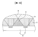
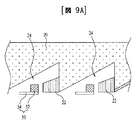
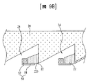
一例として、導光板20の溝24が断面三角形の場合、互いに相対し、頂点で会う第1及び第2側面のうち、溝の第1側面は、導光板20の上部面に平行な水平面と垂直であり、溝の第2側面は、導光板20の上部面に平行な水平面に対して傾斜すればよい。
このような暗部26は、導光板20の側面24bから前方約3〜5mmの距離にわたって現れることがある。
Claims (27)
- 溝を有する導光板と、
前記導光板の溝に配置された光源モジュールと、
前記導光板の溝の側面から前記光源モジュールの方向に突出し、前記光源モジュールで生成された光を前記導光板に導く突出部と
を備え、
前記突出部は
前記光源モジュールに面する第1側面と、
前記溝の側面に面する第2側面とを有し、
前記突出部の長さは、前記第1側面と前記第2側面との間の前記光源モジュール方向への第1距離に該当し、
前記光源モジュールは、前記光源モジュール方向と異なる方向に配列された複数の光源を有し、
前記複数の光源のうち、隣接した光源は互いに第2距離だけ離隔しており、
前記突出部の長さは、前記第2距離が小さいほど短くなっており、第2距離が大きいほど長くなっている、ディスプレイ装置。 - 前記第1側面の面積は前記第2側面の面積よりも小さい、請求項1に記載のディスプレイ装置。
- 前記突出部の第1側面の高さと前記第2側面の高さの比は1:1〜3である、請求項2に記載のディスプレイ装置。
- 前記突出部の第1側面の高さは、前記光源モジュールの光源の高さよりも高い、請求項2又は3に記載のディスプレイ装置。
- 前記突出部の第1側面の高さと前記光源モジュールの光源の高さは互いに同一である、
請求項2に記載のディスプレイ装置。 - 前記突出部の第1側面は前記光源モジュールの光源から離隔する、請求項2乃至5のいずれかに記載のディスプレイ装置。
- 前記突出部の第1側面は前記光源モジュールの光源に接触する、請求項2乃至5のいずれかに記載のディスプレイ装置。
- 前記突出部の第2側面の高さと前記導光板の溝の高さとの比は1:1〜3である、請求項2に記載のディスプレイ装置。
- 前記導光板及び突出部は互いに同一の物質で構成されている、請求項1に記載のディスプレイ装置。
- 前記導光板及び突出部は、互いに異なる物質で構成されている、請求項1に記載のディスプレイ装置。
- 前記光源モジュールは光源の配列された基板を備え、前記基板は、前記突出部の下部面
に配置されている、請求項1に記載のディスプレイ装置。 - 前記導光板及び突出部は、PMMA(Polymethylmethacrylate)、PET(polyethyleneterephthlate)、COC(Cyclic Olefin Copolymers)、PEN(polyethylenenaphthalate)、PC(Polycarbonate)、PS(Polystyrene)、MS(Mathacylate styrene)のいずれか1つからなる、
請求項1乃至11のいずれかに記載のディスプレイ装置。 - 前記突出部は、前記溝の側面から前記光源モジュールの方向に1〜10mm長さだけ突出する、請求項1乃至11のいずれかに記載のディスプレイ装置。
- 前記突出部の上部面及び下部面の少なくとも一方は、前記溝の側面に垂直な平面である、または、前記溝の側面に対して所定角度で傾斜した傾斜面である、請求項1乃至11のいずれかに記載のディスプレイ装置。
- 前記突出部の上部面及び下部面は互いに平行である、請求項3乃至11のいずれかに記載のディスプレイ装置。
- 前記導光板の溝の高さと前記導光板の厚さとの比は0.3〜0.9:1である、請求項1乃至11のいずれかに記載のディスプレイ装置。
- 前記突出部の上部面または前記導光板の溝の内面のうちの少なくとも一方に第2リフレクタが配置されている、請求項1乃至11のいずれかに記載のディスプレイ装置。
- 前記第2リフレクタは凹凸パターンを有する、請求項17に記載のディスプレイ装置。
- 前記突出部の上部面は、水平面に対して第1角度で傾斜し、前記突出部の下部面は、水平面に対して第2角度で傾斜し、前記第1角度及び第2角度は互いに異なる、請求項1乃至6のいずれかに記載のディスプレイ装置。
- 前記第1角度は前記第2角度よりも大きい、請求項19に記載のディスプレイ装置。
- 前記導光板の溝内に配置され、前記光源モジュールを固定するストッパーをさらに備える、請求項1に記載のディスプレイ装置。
- 前記光源モジュールは、
前記導光板と第1方向に向かい合う上面を有する基板と、
前記基板の上面上に配置された複数の光源と、
を備える、請求項1に記載のディスプレイ装置。 - 前記突出部は、前記第1方向と垂直な第2方向に突出している、請求項22に記載のディスプレイ装置。
- 前記基板の上面上に配置された第1リフレクタをさらに備える、請求項22に記載のディスプレイ装置。
- 前記第1リフレクタは凹凸パターンを有する、請求項24に記載のディスプレイ装置。
- 前記突出部の前記第1及び第2側面間の前記第1距離は、前記隣接した光源間の第2距離と異なる、請求項1に記載のディスプレイ装置。
- ディスプレイパネルをさらに備える、請求項1乃至26のいずれかに記載のディスプレイ装置。
Applications Claiming Priority (2)
| Application Number | Priority Date | Filing Date | Title |
|---|---|---|---|
| KR10-2011-0064747 | 2011-06-30 | ||
| KR1020110064747A KR101824036B1 (ko) | 2011-06-30 | 2011-06-30 | 디스플레이 장치 |
Publications (3)
| Publication Number | Publication Date |
|---|---|
| JP2013016459A JP2013016459A (ja) | 2013-01-24 |
| JP2013016459A5 JP2013016459A5 (ja) | 2015-03-19 |
| JP5959868B2 true JP5959868B2 (ja) | 2016-08-02 |
Family
ID=45841373
Family Applications (1)
| Application Number | Title | Priority Date | Filing Date |
|---|---|---|---|
| JP2012029679A Expired - Fee Related JP5959868B2 (ja) | 2011-06-30 | 2012-02-14 | バックライトユニット及びそれを用いたディスプレイ装置 |
Country Status (6)
| Country | Link |
|---|---|
| US (1) | US8915639B2 (ja) |
| EP (1) | EP2541136B1 (ja) |
| JP (1) | JP5959868B2 (ja) |
| KR (1) | KR101824036B1 (ja) |
| CN (1) | CN102853328A (ja) |
| TW (1) | TWI594051B (ja) |
Families Citing this family (8)
| Publication number | Priority date | Publication date | Assignee | Title |
|---|---|---|---|---|
| KR101529558B1 (ko) * | 2013-05-23 | 2015-06-17 | 엘지디스플레이 주식회사 | 액정표시소자 |
| WO2016075737A1 (ja) * | 2014-11-10 | 2016-05-19 | 株式会社ワンダーフューチャーコーポレーション | タッチパネル、タッチパネルの製造方法、及びタッチパネル一体型表示装置 |
| JP6827635B2 (ja) * | 2016-12-09 | 2021-02-10 | 日亜化学工業株式会社 | 面光源装置、表示装置及び電子機器 |
| US20180306960A1 (en) * | 2017-04-25 | 2018-10-25 | Wuhan China Star Optoelectronics Technology Co., Ltd. | Backlight modules and liquid crystal displays |
| WO2019201729A1 (en) * | 2018-04-18 | 2019-10-24 | Lumileds Holding B.V. | Segmented backlight structure with in-coupling structures |
| KR102785601B1 (ko) * | 2018-12-26 | 2025-03-26 | 엘지이노텍 주식회사 | 조명 모듈, 조명 장치 및 그 제조방법 |
| KR102884668B1 (ko) * | 2019-08-01 | 2025-11-11 | 엘지이노텍 주식회사 | 조명 장치 |
| US11874562B2 (en) * | 2021-12-07 | 2024-01-16 | Huizhou China Star Optoelectronics Display Co., Ltd. | Component for dissipating heat of device, backlight module, and display panel |
Family Cites Families (27)
| Publication number | Priority date | Publication date | Assignee | Title |
|---|---|---|---|---|
| JP2000267093A (ja) * | 1999-03-19 | 2000-09-29 | Matsushita Electric Ind Co Ltd | 照明装置およびこれを備えた携帯情報機器 |
| JP4262368B2 (ja) * | 1999-09-22 | 2009-05-13 | 株式会社日立製作所 | 照明装置、及びこれを用いた表示装置 |
| JP2001312916A (ja) * | 2000-02-24 | 2001-11-09 | Sony Corp | 面光源装置 |
| JP4413455B2 (ja) * | 2001-08-09 | 2010-02-10 | 日本ライツ株式会社 | 導光板および平面照明装置 |
| US6948840B2 (en) | 2001-11-16 | 2005-09-27 | Everbrite, Llc | Light emitting diode light bar |
| JP2004095390A (ja) * | 2002-08-30 | 2004-03-25 | Fujitsu Display Technologies Corp | 照明装置及び表示装置 |
| DE102004046696A1 (de) * | 2004-05-24 | 2005-12-29 | Osram Opto Semiconductors Gmbh | Verfahren zur Montage eines Oberflächenleuchtsystems und Oberflächenleuchtsystem |
| WO2008032277A2 (en) | 2006-09-15 | 2008-03-20 | Koninklijke Philips Electronics N.V. | Flat and thin led-based luminary providing collimated light |
| TW200900766A (en) * | 2007-02-21 | 2009-01-01 | Koninkl Philips Electronics Nv | Lighting system with improved rigidity |
| DE102007042104A1 (de) * | 2007-09-05 | 2009-03-12 | Osram Opto Semiconductors Gmbh | Display-Anordnung sowie Verfahren zur Ansteuerung einer Displayeinheit einer Displayanordnung |
| KR101565934B1 (ko) * | 2008-05-23 | 2015-11-06 | 삼성디스플레이 주식회사 | 백라이트 어셈블리 및 이를 갖는 표시장치 |
| WO2009145548A2 (en) * | 2008-05-27 | 2009-12-03 | Lg Electronics Inc. | Led back-light unit and liquid crystal display device using the same |
| US8220981B2 (en) * | 2008-05-27 | 2012-07-17 | Lg Electronics Inc. | Liquid crystal display having a plurality of modules |
| US8360592B2 (en) * | 2008-09-29 | 2013-01-29 | Seoul Semiconductor Co., Ltd. | Backlight unit and display apparatus having the same |
| US20110164404A1 (en) * | 2008-09-30 | 2011-07-07 | Sharp Kabushiki Kaisha | Illumination device, surface light source device, and liquid crystal display apparatus |
| WO2010038808A1 (ja) * | 2008-09-30 | 2010-04-08 | シャープ株式会社 | 照明装置および液晶表示装置 |
| KR20100054209A (ko) * | 2008-11-14 | 2010-05-25 | 엘지이노텍 주식회사 | 액정표시장치 및 도광판의 제조방법 |
| TW200938909A (en) | 2009-03-13 | 2009-09-16 | Global Lighting Technologies Taiwan Inc | Section light-guide structure of light-guide plate |
| JP2011023139A (ja) * | 2009-07-13 | 2011-02-03 | Sharp Corp | 導光体、照明ユニット、バックライト装置および表示装置 |
| KR101255287B1 (ko) * | 2009-07-16 | 2013-04-15 | 엘지디스플레이 주식회사 | 백라이트 유닛 |
| KR20110011463A (ko) * | 2009-07-28 | 2011-02-08 | 엘지이노텍 주식회사 | 라이트 유닛 및 이를 구비한 표시장치 |
| KR101611616B1 (ko) * | 2009-08-28 | 2016-04-11 | 엘지전자 주식회사 | 백라이트 유닛 및 그를 이용한 디스플레이 장치 |
| JP5492519B2 (ja) * | 2009-10-02 | 2014-05-14 | 日立コンシューマエレクトロニクス株式会社 | バックライトユニットおよびそれを用いた映像表示装置 |
| JP2011107229A (ja) * | 2009-11-13 | 2011-06-02 | Sony Ericsson Mobile Communications Ab | 液晶モジュールおよび電子機器 |
| WO2011115351A1 (en) * | 2010-03-15 | 2011-09-22 | Lg Electronics Inc. | Backlight unit and display apparatus including the same |
| US8646932B2 (en) * | 2010-06-15 | 2014-02-11 | Lg Innotek Co., Ltd. | Backlight unit and the display device having the same |
| JP2012119246A (ja) * | 2010-12-03 | 2012-06-21 | Hitachi Consumer Electronics Co Ltd | バックライト装置及びこれを用いた映像表示装置 |
-
2011
- 2011-06-30 KR KR1020110064747A patent/KR101824036B1/ko not_active Expired - Fee Related
-
2012
- 2012-02-14 JP JP2012029679A patent/JP5959868B2/ja not_active Expired - Fee Related
- 2012-02-14 US US13/396,108 patent/US8915639B2/en active Active
- 2012-02-21 TW TW101105617A patent/TWI594051B/zh not_active IP Right Cessation
- 2012-02-27 CN CN2012100478372A patent/CN102853328A/zh active Pending
- 2012-03-19 EP EP12160155.3A patent/EP2541136B1/en active Active
Also Published As
| Publication number | Publication date |
|---|---|
| KR101824036B1 (ko) | 2018-03-14 |
| TW201300901A (zh) | 2013-01-01 |
| JP2013016459A (ja) | 2013-01-24 |
| EP2541136B1 (en) | 2019-05-08 |
| US20130003353A1 (en) | 2013-01-03 |
| EP2541136A1 (en) | 2013-01-02 |
| TWI594051B (zh) | 2017-08-01 |
| US8915639B2 (en) | 2014-12-23 |
| KR20130003407A (ko) | 2013-01-09 |
| CN102853328A (zh) | 2013-01-02 |
Similar Documents
| Publication | Publication Date | Title |
|---|---|---|
| JP6042072B2 (ja) | ディスプレイ装置 | |
| JP6029837B2 (ja) | バックライトユニット及びそれを用いたディスプレイ装置 | |
| JP6062083B2 (ja) | 照明システム | |
| JP5959868B2 (ja) | バックライトユニット及びそれを用いたディスプレイ装置 | |
| JP5999917B2 (ja) | バックライトユニット及びそれを用いたディスプレイ装置 | |
| JP6087508B2 (ja) | バックライトユニット及びそれを用いたディスプレイ装置 | |
| KR20130039406A (ko) | 백라이트 유닛 및 이를 이용한 디스플레이 장치 | |
| KR20130000903A (ko) | 백라이트 유닛 및 그를 이용한 디스플레이 장치 | |
| KR101874902B1 (ko) | 백라이트 유닛 및 그를 이용한 디스플레이 장치 | |
| KR101838020B1 (ko) | 조명 장치 | |
| KR101820693B1 (ko) | 백라이트 유닛 및 그를 이용한 디스플레이 장치 | |
| KR20120112989A (ko) | 백라이트 유닛 및 그를 이용한 표시장치 |
Legal Events
| Date | Code | Title | Description |
|---|---|---|---|
| A521 | Request for written amendment filed |
Free format text: JAPANESE INTERMEDIATE CODE: A523 Effective date: 20150130 |
|
| A621 | Written request for application examination |
Free format text: JAPANESE INTERMEDIATE CODE: A621 Effective date: 20150130 |
|
| A977 | Report on retrieval |
Free format text: JAPANESE INTERMEDIATE CODE: A971007 Effective date: 20151207 |
|
| A131 | Notification of reasons for refusal |
Free format text: JAPANESE INTERMEDIATE CODE: A131 Effective date: 20151215 |
|
| A521 | Request for written amendment filed |
Free format text: JAPANESE INTERMEDIATE CODE: A523 Effective date: 20160310 |
|
| TRDD | Decision of grant or rejection written | ||
| A01 | Written decision to grant a patent or to grant a registration (utility model) |
Free format text: JAPANESE INTERMEDIATE CODE: A01 Effective date: 20160614 |
|
| A61 | First payment of annual fees (during grant procedure) |
Free format text: JAPANESE INTERMEDIATE CODE: A61 Effective date: 20160622 |
|
| R150 | Certificate of patent or registration of utility model |
Ref document number: 5959868 Country of ref document: JP Free format text: JAPANESE INTERMEDIATE CODE: R150 |
|
| R250 | Receipt of annual fees |
Free format text: JAPANESE INTERMEDIATE CODE: R250 |
|
| R250 | Receipt of annual fees |
Free format text: JAPANESE INTERMEDIATE CODE: R250 |
|
| R250 | Receipt of annual fees |
Free format text: JAPANESE INTERMEDIATE CODE: R250 |
|
| S531 | Written request for registration of change of domicile |
Free format text: JAPANESE INTERMEDIATE CODE: R313531 |
|
| S111 | Request for change of ownership or part of ownership |
Free format text: JAPANESE INTERMEDIATE CODE: R313113 |
|
| R350 | Written notification of registration of transfer |
Free format text: JAPANESE INTERMEDIATE CODE: R350 |
|
| R350 | Written notification of registration of transfer |
Free format text: JAPANESE INTERMEDIATE CODE: R350 |
|
| R250 | Receipt of annual fees |
Free format text: JAPANESE INTERMEDIATE CODE: R250 |
|
| R250 | Receipt of annual fees |
Free format text: JAPANESE INTERMEDIATE CODE: R250 |
|
| LAPS | Cancellation because of no payment of annual fees |