JP5977830B2 - 異なるエッチングレートに基づくpチャネル又はnチャネルデバイスの区別についての方法 - Google Patents
異なるエッチングレートに基づくpチャネル又はnチャネルデバイスの区別についての方法 Download PDFInfo
- Publication number
- JP5977830B2 JP5977830B2 JP2014531322A JP2014531322A JP5977830B2 JP 5977830 B2 JP5977830 B2 JP 5977830B2 JP 2014531322 A JP2014531322 A JP 2014531322A JP 2014531322 A JP2014531322 A JP 2014531322A JP 5977830 B2 JP5977830 B2 JP 5977830B2
- Authority
- JP
- Japan
- Prior art keywords
- cesl
- fet
- layer
- image
- cmos
- Prior art date
- Legal status (The legal status is an assumption and is not a legal conclusion. Google has not performed a legal analysis and makes no representation as to the accuracy of the status listed.)
- Expired - Fee Related
Links
- 238000000034 method Methods 0.000 title claims description 130
- 238000005530 etching Methods 0.000 title claims description 33
- 230000008569 process Effects 0.000 claims description 74
- 239000000463 material Substances 0.000 claims description 24
- 239000004065 semiconductor Substances 0.000 claims description 14
- XUIMIQQOPSSXEZ-UHFFFAOYSA-N Silicon Chemical compound [Si] XUIMIQQOPSSXEZ-UHFFFAOYSA-N 0.000 claims description 11
- 229910044991 metal oxide Inorganic materials 0.000 claims description 11
- 150000004706 metal oxides Chemical class 0.000 claims description 11
- 229910052710 silicon Inorganic materials 0.000 claims description 11
- 239000010703 silicon Substances 0.000 claims description 11
- 238000001312 dry etching Methods 0.000 claims description 9
- 238000001039 wet etching Methods 0.000 claims description 9
- 238000005498 polishing Methods 0.000 claims description 7
- QTBSBXVTEAMEQO-UHFFFAOYSA-N Acetic acid Chemical compound CC(O)=O QTBSBXVTEAMEQO-UHFFFAOYSA-N 0.000 claims description 6
- 239000000126 substance Substances 0.000 claims description 6
- 230000000295 complement effect Effects 0.000 claims description 5
- 239000000758 substrate Substances 0.000 claims description 5
- KRHYYFGTRYWZRS-UHFFFAOYSA-N Fluorane Chemical compound F KRHYYFGTRYWZRS-UHFFFAOYSA-N 0.000 claims description 4
- 239000012811 non-conductive material Substances 0.000 claims description 4
- 238000004519 manufacturing process Methods 0.000 claims description 2
- 239000000203 mixture Substances 0.000 claims description 2
- XLYOFNOQVPJJNP-UHFFFAOYSA-N water Substances O XLYOFNOQVPJJNP-UHFFFAOYSA-N 0.000 claims description 2
- 241001481833 Coryphaena hippurus Species 0.000 claims 1
- 239000010410 layer Substances 0.000 description 236
- 229910052751 metal Inorganic materials 0.000 description 117
- 239000002184 metal Substances 0.000 description 117
- 238000004458 analytical method Methods 0.000 description 44
- 238000013461 design Methods 0.000 description 44
- 230000006870 function Effects 0.000 description 23
- 230000004888 barrier function Effects 0.000 description 15
- 238000001000 micrograph Methods 0.000 description 10
- 229910021420 polycrystalline silicon Inorganic materials 0.000 description 10
- 238000000354 decomposition reaction Methods 0.000 description 9
- 238000010586 diagram Methods 0.000 description 9
- 230000033001 locomotion Effects 0.000 description 9
- 230000003287 optical effect Effects 0.000 description 9
- 238000000605 extraction Methods 0.000 description 8
- 238000003384 imaging method Methods 0.000 description 8
- 238000012545 processing Methods 0.000 description 8
- 238000003860 storage Methods 0.000 description 8
- 229920005591 polysilicon Polymers 0.000 description 7
- 238000011835 investigation Methods 0.000 description 6
- 238000002372 labelling Methods 0.000 description 6
- 238000002161 passivation Methods 0.000 description 5
- XAGFODPZIPBFFR-UHFFFAOYSA-N aluminium Chemical compound [Al] XAGFODPZIPBFFR-UHFFFAOYSA-N 0.000 description 4
- 230000014509 gene expression Effects 0.000 description 4
- 238000009413 insulation Methods 0.000 description 4
- 238000005259 measurement Methods 0.000 description 4
- 230000000644 propagated effect Effects 0.000 description 4
- WFKWXMTUELFFGS-UHFFFAOYSA-N tungsten Chemical compound [W] WFKWXMTUELFFGS-UHFFFAOYSA-N 0.000 description 4
- 229910052721 tungsten Inorganic materials 0.000 description 4
- 239000010937 tungsten Substances 0.000 description 4
- 235000012431 wafers Nutrition 0.000 description 4
- 230000004913 activation Effects 0.000 description 3
- 238000001994 activation Methods 0.000 description 3
- 229910052782 aluminium Inorganic materials 0.000 description 3
- 230000000694 effects Effects 0.000 description 3
- 230000005669 field effect Effects 0.000 description 3
- 239000011229 interlayer Substances 0.000 description 3
- 238000004091 panning Methods 0.000 description 3
- 238000001020 plasma etching Methods 0.000 description 3
- 230000004044 response Effects 0.000 description 3
- 230000011664 signaling Effects 0.000 description 3
- RYGMFSIKBFXOCR-UHFFFAOYSA-N Copper Chemical compound [Cu] RYGMFSIKBFXOCR-UHFFFAOYSA-N 0.000 description 2
- VYPSYNLAJGMNEJ-UHFFFAOYSA-N Silicium dioxide Chemical compound O=[Si]=O VYPSYNLAJGMNEJ-UHFFFAOYSA-N 0.000 description 2
- 230000009471 action Effects 0.000 description 2
- 239000000654 additive Substances 0.000 description 2
- 230000000996 additive effect Effects 0.000 description 2
- 230000008859 change Effects 0.000 description 2
- 238000001311 chemical methods and process Methods 0.000 description 2
- 229910052802 copper Inorganic materials 0.000 description 2
- 239000010949 copper Substances 0.000 description 2
- 230000008878 coupling Effects 0.000 description 2
- 238000010168 coupling process Methods 0.000 description 2
- 238000005859 coupling reaction Methods 0.000 description 2
- 238000005516 engineering process Methods 0.000 description 2
- 239000000284 extract Substances 0.000 description 2
- 230000002452 interceptive effect Effects 0.000 description 2
- 150000002500 ions Chemical class 0.000 description 2
- 238000007521 mechanical polishing technique Methods 0.000 description 2
- 230000005499 meniscus Effects 0.000 description 2
- 150000002739 metals Chemical class 0.000 description 2
- 230000004048 modification Effects 0.000 description 2
- 238000012986 modification Methods 0.000 description 2
- 238000005268 plasma chemical vapour deposition Methods 0.000 description 2
- 230000005855 radiation Effects 0.000 description 2
- 239000002356 single layer Substances 0.000 description 2
- 230000000007 visual effect Effects 0.000 description 2
- 229910018503 SF6 Inorganic materials 0.000 description 1
- 229910004298 SiO 2 Inorganic materials 0.000 description 1
- 241000519995 Stachys sylvatica Species 0.000 description 1
- 239000002253 acid Substances 0.000 description 1
- 150000007513 acids Chemical class 0.000 description 1
- 238000013459 approach Methods 0.000 description 1
- 230000008901 benefit Effects 0.000 description 1
- 230000002457 bidirectional effect Effects 0.000 description 1
- 238000004891 communication Methods 0.000 description 1
- 238000005520 cutting process Methods 0.000 description 1
- 238000013500 data storage Methods 0.000 description 1
- 230000000994 depressogenic effect Effects 0.000 description 1
- 238000001493 electron microscopy Methods 0.000 description 1
- 239000007789 gas Substances 0.000 description 1
- 239000011521 glass Substances 0.000 description 1
- 239000011810 insulating material Substances 0.000 description 1
- 238000005468 ion implantation Methods 0.000 description 1
- 238000012804 iterative process Methods 0.000 description 1
- 239000007788 liquid Substances 0.000 description 1
- 239000004973 liquid crystal related substance Substances 0.000 description 1
- 238000011068 loading method Methods 0.000 description 1
- 238000004518 low pressure chemical vapour deposition Methods 0.000 description 1
- 239000003550 marker Substances 0.000 description 1
- 238000012544 monitoring process Methods 0.000 description 1
- TWNQGVIAIRXVLR-UHFFFAOYSA-N oxo(oxoalumanyloxy)alumane Chemical compound O=[Al]O[Al]=O TWNQGVIAIRXVLR-UHFFFAOYSA-N 0.000 description 1
- 238000004806 packaging method and process Methods 0.000 description 1
- 238000000623 plasma-assisted chemical vapour deposition Methods 0.000 description 1
- 238000001878 scanning electron micrograph Methods 0.000 description 1
- 238000000926 separation method Methods 0.000 description 1
- 235000012239 silicon dioxide Nutrition 0.000 description 1
- 239000000377 silicon dioxide Substances 0.000 description 1
- 239000007787 solid Substances 0.000 description 1
- 238000004544 sputter deposition Methods 0.000 description 1
- SFZCNBIFKDRMGX-UHFFFAOYSA-N sulfur hexafluoride Chemical compound FS(F)(F)(F)(F)F SFZCNBIFKDRMGX-UHFFFAOYSA-N 0.000 description 1
- 229960000909 sulfur hexafluoride Drugs 0.000 description 1
Images


Classifications
-
- G—PHYSICS
- G01—MEASURING; TESTING
- G01R—MEASURING ELECTRIC VARIABLES; MEASURING MAGNETIC VARIABLES
- G01R31/00—Arrangements for testing electric properties; Arrangements for locating electric faults; Arrangements for electrical testing characterised by what is being tested not provided for elsewhere
- G01R31/28—Testing of electronic circuits, e.g. by signal tracer
- G01R31/302—Contactless testing
- G01R31/305—Contactless testing using electron beams
- G01R31/307—Contactless testing using electron beams of integrated circuits
-
- G—PHYSICS
- G01—MEASURING; TESTING
- G01R—MEASURING ELECTRIC VARIABLES; MEASURING MAGNETIC VARIABLES
- G01R31/00—Arrangements for testing electric properties; Arrangements for locating electric faults; Arrangements for electrical testing characterised by what is being tested not provided for elsewhere
- G01R31/28—Testing of electronic circuits, e.g. by signal tracer
- G01R31/2851—Testing of integrated circuits [IC]
- G01R31/2898—Sample preparation, e.g. removing encapsulation, etching
Landscapes
- Engineering & Computer Science (AREA)
- Computer Hardware Design (AREA)
- Microelectronics & Electronic Packaging (AREA)
- General Engineering & Computer Science (AREA)
- Physics & Mathematics (AREA)
- General Physics & Mathematics (AREA)
- Metal-Oxide And Bipolar Metal-Oxide Semiconductor Integrated Circuits (AREA)
- Testing Or Measuring Of Semiconductors Or The Like (AREA)
- Weting (AREA)
Description
(背景)
(発明の分野)
本出願の主題は、半導体集積回路に関し、より具体的には、既に存在しているCMOS集積回路上のデバイスがpチャネルデバイスかnチャネルデバイスかを特定することに関する。
集積回路(IC)は、pタイプ領域用の過剰ホール及びnタイプ領域用の過剰電子を与えるようにドープが行われたアクティブ領域(複数)を備えるシリコンウェハ上に形成されることが多い。アクティブ領域は、pチャネル金属酸化物電界効果トランジスタ(p-MOSFET、PMOS、又は p-FET)及び又はnチャネル金属酸化物電界効果トランジスタ(n-MOSFET、NMOS、又は n-FET)を形成するように配することができる。或る場合には、アクティブ領域は、当該アクティブ領域(複数)とシリコンウェハとの間に配された二酸化シリコン(SiO2)のような非導電層上に形成される。集積回路の多くは、p−FETとn−FETの両者を設計に組み込んだ相補型金属酸化物半導体(CMOS、complimentary metal-oxide semiconductor)回路を利用する。
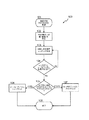
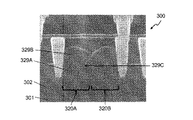
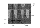
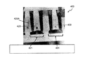
相補型金属酸化物半導体(CMOS)集積回路(IC)を調査する方法についての種々の実施形態は、コンタクトエッチストップ層(CESL、contact etch stop layer)の上にあるCMOS ICの少なくとも少量の材料を除去することと、次にそのCMOS ICを或る時間長さにわたってエッチングして、そのCESLの少なくとも少量を除去することを含み得る。その後に、そのCMOS ICの詳細が精査されて、CESLの領域が区別され得る。CESLの上記区別された領域に基づいて、そのCMOS ICの第1の領域が、pチャネル金属酸化物半導体(p-FET)デバイスを含むものとして特定され、そのCMOS ICの第2の領域が、nチャネル金属酸化物半導体(n-FET)デバイスを含むものとして特定され得る。
本明細書に組み込まれその一部を構成する添付図面は、本発明の種々の実施形態を例示するものである。これらの図は、概要説明と共に、種々の実施形態の原理を説明するのに役立つ。これらの図面において:
以下に示す詳細な説明では、種々の実施形態を完全に理解できるように、多数の具体的詳細が例として示されている。しかしながら、ここに記載された実施例をそのような詳細を用いずに実施できることは、当業者にとり明らかである。他の例示では、本概念について不要な曖昧さが生じるのを避けるべく、周知の方法、手順、及びコンポーネントが、比較的高いレベルで、詳細を示すことなく記載されている。ここに開示する種々の実施形態の説明においては、多くの記述的な用語やフレーズが用いられている。これらの記述的な用語やフレーズは、本明細書において他の定義が示されている場合を除き、当業者において一般的に認められている意味を伝えるべく用いられている。記述的用語及びフレーズの一部については、その意味を明確にすべく、以下の段落(複数)において説明されている。次に、添付図面に示した例を参照しつつ、以下に詳細に説明する。
ロックステップの動きは、残像効果(trailing effect)として図中に示される。
アノテーションオブジェクトは、編集操作を開始したモザイクビューに表示されているアノテーションオーバレイに関連付けられる;
アノテーションオブジェクトの移動やコピーを行うと、そのアノテーションオブジェクトは、編集操作を終了したモザイクビューに表示されているアノテーションオーバレイに関連付けられる。
Claims (18)
- 相補型金属酸化物半導体(CMOS)集積回路(IC)を調査する方法であって、
コンタクトエッチストップ層(CESL)の上の、前記CMOS−ICの材料の少なくとも少量を除去して、当該CMOS−ICの一の領域における前記CESLの少なくとも一部分を露出させるステップと、
前記CMOS−ICの前記領域をエッチングして、当該領域内に前記CESLの少なくとも少量が残存するように前記CESLの前記露出された部分を部分的に除去するステップと、
前記領域内に残存するCESLの状態を精査してCESLの領域を区別するステップと、
CESLの前記区別された領域に基づき、pチャネル金属酸化物半導体デバイス(p−FET)を含むCMOS−ICの第1の領域と、nチャネル金属酸化物半導体デバイス(n−FET)を含むCMOS−ICの第2の領域と、を特定するステップと、
を有する、方法。 - 前記CMOS−ICに用いられたものと同じ作製プロセスを用いて形成されたn−FETとp−FETと、を有するデバイスの、断面を作成するステップと、
前記断面を精査して、前記断面を生成したデバイスの、n−FETとは異なるp−FETのCESL特性を特定するステップと、
を更に有する、請求項1に記載の方法。 - 前記CESLの厚さを測定するステップと、
前記CESLの前記測定された厚さに基づいて、前記CMOS−ICの前記領域をエッチングする時間長さを決定するステップと、
を更に有する、請求項2に記載の方法。 - 前記材料の少なくとも少量の前記除去は、ウェットエッチング、ドライエッチング、化学機械研磨(CMP)、化学研磨、及び機械研磨で構成されるグループから選択された少なくとも一つのプロセスを含む、
請求項1に記載の方法。 - 前記時間長さは、予め定められた所定の時間期間である、請求項3に記載の方法。
- 前記所定の時間期間は、30秒と60秒との間である、請求項5に記載の方法。
- p−FETを覆うCESLのエリアからn−FETを覆うCESLのエリアを区別できる程度に、前記CESLが十分にエッチング除去されているか否かを判断するステップと、
前記CESLが未だ十分にエッチング除去されていないと判断されるときに、前記CMOS−ICを、他の時間期間にわたり再度エッチングし、前記CESLの更に少なくとも少量を除去するステップと、
を更に有する、請求項1に記載の方法。 - 前記他の時間期間は前記時間長さ以下である、請求項7に記載の方法。
- 前記エッチングはウェットエッチ・プロセスを用いる、請求項1に記載の方法。
- 前記ウェットエッチ・プロセスは、水、フッ化水素酸、及び酢酸の混合液を用いる、請求項9に記載の方法。
- CMOS−ICの前記精査は走査型電子顕微鏡を用いて行われる、請求項1に記載の方法。
- 前記第1の領域と前記第2の領域を特定する前記ステップは、
第1の特性を有するCESLに関連する第1のデバイスフットプリントを見つけ出すステップと、
第2の特性を有するCESLに関連する第2のデバイスフットプリントを見つけ出すステップと、
前記第1のデバイスフットプリントを前記第1の領域として特定し、前記第2のデバイスフットプリントを前記第2の領域として特定するステップと、
を有する、請求項1に記載の方法。 - 前記第1の特性はCESLの第1の量が残存することであり、前記第2の特性はCESLの第2の量が残存することであって、
CESLの前記第2の量は、CESLの前記第1の量よりも少ない、
請求項12に記載の方法。 - CESLの前記第2の量はゼロである、請求項13に記載の方法。
- 前記第1の領域と前記第2の領域とを特定する前記ステップは、
少なくとも少量のCESLが残存する第1のデバイスフットプリントを見つけ出すステップと、
CESLが何も残っていない第2のデバイスフットプリントを見つけ出すステップと、
前記第1のデバイスフットプリントを前記第1の領域として特定し、前記第2のデバイスフットプリントを前記第2の領域として特定するステップと、
を有する、請求項1に記載の方法。 - 前記第1の領域と前記第2の領域とを特定する前記ステップは、
CESLが殆ど乃至全く残っていない第1のデバイスフットプリントを見つけ出すステップと、
第1のデバイスフットプリントより多くのCESLが残存する第2のデバイスフットプリントを見つけ出すステップと、
前記第1のデバイスフットプリントを前記第1の領域として特定し、前記第2のデバイスフットプリントを前記第2の領域として特定するステップと、
を有する、請求項1に記載の方法。 - 前記CMOS−ICは、n−FETとp−FETとを有し、当該n−FETと当該p−FETは、共に非導電材料の層の上面上に形成されている、
請求項1に記載の方法。 - 前記非導電材料の層は、シリコンの基板の上面上にある、
請求項17に記載の方法。
Applications Claiming Priority (1)
| Application Number | Priority Date | Filing Date | Title |
|---|---|---|---|
| PCT/IB2011/054245 WO2013045973A1 (en) | 2011-09-27 | 2011-09-27 | A method to differential p-channel or n-channel devices based on different etching rates. |
Publications (2)
| Publication Number | Publication Date |
|---|---|
| JP2014531763A JP2014531763A (ja) | 2014-11-27 |
| JP5977830B2 true JP5977830B2 (ja) | 2016-08-24 |
Family
ID=47994345
Family Applications (1)
| Application Number | Title | Priority Date | Filing Date |
|---|---|---|---|
| JP2014531322A Expired - Fee Related JP5977830B2 (ja) | 2011-09-27 | 2011-09-27 | 異なるエッチングレートに基づくpチャネル又はnチャネルデバイスの区別についての方法 |
Country Status (7)
| Country | Link |
|---|---|
| EP (1) | EP2764376B1 (ja) |
| JP (1) | JP5977830B2 (ja) |
| KR (1) | KR20140082993A (ja) |
| CN (1) | CN104105976B (ja) |
| CA (1) | CA2849729A1 (ja) |
| PL (1) | PL2764376T3 (ja) |
| WO (1) | WO2013045973A1 (ja) |
Families Citing this family (2)
| Publication number | Priority date | Publication date | Assignee | Title |
|---|---|---|---|---|
| KR102260931B1 (ko) * | 2017-05-15 | 2021-06-04 | 엘피케이에프 레이저 앤드 일렉트로닉스 악티엔게젤샤프트 | 레이저 유도 디프 반응성 에칭을 이용해 기판을 가공하기 위한, 특히 분리하기 위한 방법 |
| JP2020131141A (ja) * | 2019-02-21 | 2020-08-31 | 紀州技研工業株式会社 | 描画方法および描画装置 |
Family Cites Families (13)
| Publication number | Priority date | Publication date | Assignee | Title |
|---|---|---|---|---|
| US4623255A (en) * | 1983-10-13 | 1986-11-18 | The United States Of America As Represented By The Administrator, National Aeronautics And Space Administration | Method of examining microcircuit patterns |
| JP2953020B2 (ja) * | 1990-10-05 | 1999-09-27 | 日本電気株式会社 | 半導体装置の製造方法 |
| JPH11135785A (ja) * | 1997-10-31 | 1999-05-21 | Sony Corp | 半導体装置の製造方法 |
| JP2000260768A (ja) * | 1999-03-05 | 2000-09-22 | Nec Corp | 半導体装置の製造方法 |
| US7294935B2 (en) * | 2001-01-24 | 2007-11-13 | Hrl Laboratories, Llc | Integrated circuits protected against reverse engineering and method for fabricating the same using an apparent metal contact line terminating on field oxide |
| US6872581B2 (en) * | 2001-04-16 | 2005-03-29 | Nptest, Inc. | Measuring back-side voltage of an integrated circuit |
| JP4302971B2 (ja) * | 2002-12-17 | 2009-07-29 | Necエレクトロニクス株式会社 | 半導体装置の製造方法 |
| JP2005045006A (ja) * | 2003-07-22 | 2005-02-17 | Matsushita Electric Ind Co Ltd | 半導体装置の製造方法 |
| US7015146B2 (en) * | 2004-01-06 | 2006-03-21 | International Business Machines Corporation | Method of processing backside unlayering of MOSFET devices for electrical and physical characterization including a collimated ion plasma |
| CA2521675C (en) * | 2005-09-29 | 2009-11-24 | Chipworks Inc | Method of preparing an integrated circuit die for imaging |
| US20070200179A1 (en) * | 2006-02-24 | 2007-08-30 | Taiwan Semiconductor Manufacturing Co., Ltd. | Strain enhanced CMOS architecture with amorphous carbon film and fabrication method of forming the same |
| US7745236B2 (en) * | 2006-12-21 | 2010-06-29 | Spansion Llc | Floating gate process methodology |
| US7655984B2 (en) * | 2007-06-12 | 2010-02-02 | Taiwan Semiconductor Manufacturing Company, Ltd. | Semiconductor device with discontinuous CESL structure |
-
2011
- 2011-09-27 KR KR20147011513A patent/KR20140082993A/ko not_active Withdrawn
- 2011-09-27 EP EP11873517.4A patent/EP2764376B1/en not_active Not-in-force
- 2011-09-27 CA CA2849729A patent/CA2849729A1/en not_active Abandoned
- 2011-09-27 JP JP2014531322A patent/JP5977830B2/ja not_active Expired - Fee Related
- 2011-09-27 WO PCT/IB2011/054245 patent/WO2013045973A1/en not_active Ceased
- 2011-09-27 CN CN201180075089.2A patent/CN104105976B/zh not_active Expired - Fee Related
- 2011-09-27 PL PL11873517T patent/PL2764376T3/pl unknown
Also Published As
| Publication number | Publication date |
|---|---|
| PL2764376T3 (pl) | 2017-03-31 |
| CA2849729A1 (en) | 2013-04-04 |
| EP2764376A4 (en) | 2015-06-17 |
| EP2764376B1 (en) | 2016-11-16 |
| EP2764376A1 (en) | 2014-08-13 |
| CN104105976A (zh) | 2014-10-15 |
| WO2013045973A1 (en) | 2013-04-04 |
| KR20140082993A (ko) | 2014-07-03 |
| CN104105976B (zh) | 2016-09-21 |
| JP2014531763A (ja) | 2014-11-27 |
Similar Documents
| Publication | Publication Date | Title |
|---|---|---|
| US6684379B2 (en) | Design analysis workstation for analyzing integrated circuits | |
| US7020853B2 (en) | Design analysis workstation for analyzing integrated circuits | |
| US8174522B2 (en) | Three-dimensional (3D) structure data creation method, 3D structure data creation apparatus, computer-readable record media and computer system | |
| US8178837B2 (en) | Logical CAD navigation for device characteristics evaluation system | |
| JP5977830B2 (ja) | 異なるエッチングレートに基づくpチャネル又はnチャネルデバイスの区別についての方法 | |
| JP4700890B2 (ja) | 特徴整列のためのロック・ステップ・カーソル | |
| TWI844033B (zh) | 電腦系統、尺寸計測方法、及記憶媒體 | |
| CN115698627B (zh) | 图案检查/测量装置、图案检查/测量程序产品 | |
| US20050226521A1 (en) | Method and apparatus for producing a 3-D model of a semiconductor chip from mosaic images | |
| KR102801943B1 (ko) | 컴퓨터 시스템, 치수 계측 방법, 및 반도체 장치 제조 시스템 | |
| US20070031027A1 (en) | Method and system for vertically aligning tile images of an area of interest of an integrated circuit | |
| HK1058417B (en) | Man-machine interface, method and apparatus for analyzing image-mosaics |
Legal Events
| Date | Code | Title | Description |
|---|---|---|---|
| A621 | Written request for application examination |
Free format text: JAPANESE INTERMEDIATE CODE: A621 Effective date: 20140909 |
|
| A521 | Request for written amendment filed |
Free format text: JAPANESE INTERMEDIATE CODE: A523 Effective date: 20140911 |
|
| A977 | Report on retrieval |
Free format text: JAPANESE INTERMEDIATE CODE: A971007 Effective date: 20150625 |
|
| A131 | Notification of reasons for refusal |
Free format text: JAPANESE INTERMEDIATE CODE: A131 Effective date: 20150701 |
|
| A521 | Request for written amendment filed |
Free format text: JAPANESE INTERMEDIATE CODE: A523 Effective date: 20150928 |
|
| A131 | Notification of reasons for refusal |
Free format text: JAPANESE INTERMEDIATE CODE: A131 Effective date: 20160317 |
|
| A521 | Request for written amendment filed |
Free format text: JAPANESE INTERMEDIATE CODE: A523 Effective date: 20160606 |
|
| TRDD | Decision of grant or rejection written | ||
| A01 | Written decision to grant a patent or to grant a registration (utility model) |
Free format text: JAPANESE INTERMEDIATE CODE: A01 Effective date: 20160630 |
|
| A61 | First payment of annual fees (during grant procedure) |
Free format text: JAPANESE INTERMEDIATE CODE: A61 Effective date: 20160722 |
|
| R150 | Certificate of patent or registration of utility model |
Ref document number: 5977830 Country of ref document: JP Free format text: JAPANESE INTERMEDIATE CODE: R150 |
|
| R250 | Receipt of annual fees |
Free format text: JAPANESE INTERMEDIATE CODE: R250 |
|
| LAPS | Cancellation because of no payment of annual fees |