JP5985605B2 - 微分干渉計モジュールを備えたリソグラフィシステム - Google Patents
微分干渉計モジュールを備えたリソグラフィシステム Download PDFInfo
- Publication number
- JP5985605B2 JP5985605B2 JP2014502500A JP2014502500A JP5985605B2 JP 5985605 B2 JP5985605 B2 JP 5985605B2 JP 2014502500 A JP2014502500 A JP 2014502500A JP 2014502500 A JP2014502500 A JP 2014502500A JP 5985605 B2 JP5985605 B2 JP 5985605B2
- Authority
- JP
- Japan
- Prior art keywords
- beams
- mirror
- measurement
- interferometer module
- reflected
- Prior art date
- Legal status (The legal status is an assumption and is not a legal conclusion. Google has not performed a legal analysis and makes no representation as to the accuracy of the status listed.)
- Active
Links
Images


Classifications
-
- G—PHYSICS
- G01—MEASURING; TESTING
- G01B—MEASURING LENGTH, THICKNESS OR SIMILAR LINEAR DIMENSIONS; MEASURING ANGLES; MEASURING AREAS; MEASURING IRREGULARITIES OF SURFACES OR CONTOURS
- G01B9/00—Measuring instruments characterised by the use of optical techniques
- G01B9/02—Interferometers
- G01B9/02015—Interferometers characterised by the beam path configuration
- G01B9/02027—Two or more interferometric channels or interferometers
-
- G—PHYSICS
- G03—PHOTOGRAPHY; CINEMATOGRAPHY; ANALOGOUS TECHNIQUES USING WAVES OTHER THAN OPTICAL WAVES; ELECTROGRAPHY; HOLOGRAPHY
- G03F—PHOTOMECHANICAL PRODUCTION OF TEXTURED OR PATTERNED SURFACES, e.g. FOR PRINTING, FOR PROCESSING OF SEMICONDUCTOR DEVICES; MATERIALS THEREFOR; ORIGINALS THEREFOR; APPARATUS SPECIALLY ADAPTED THEREFOR
- G03F7/00—Photomechanical, e.g. photolithographic, production of textured or patterned surfaces, e.g. printing surfaces; Materials therefor, e.g. comprising photoresists; Apparatus specially adapted therefor
- G03F7/20—Exposure; Apparatus therefor
-
- G—PHYSICS
- G03—PHOTOGRAPHY; CINEMATOGRAPHY; ANALOGOUS TECHNIQUES USING WAVES OTHER THAN OPTICAL WAVES; ELECTROGRAPHY; HOLOGRAPHY
- G03F—PHOTOMECHANICAL PRODUCTION OF TEXTURED OR PATTERNED SURFACES, e.g. FOR PRINTING, FOR PROCESSING OF SEMICONDUCTOR DEVICES; MATERIALS THEREFOR; ORIGINALS THEREFOR; APPARATUS SPECIALLY ADAPTED THEREFOR
- G03F7/00—Photomechanical, e.g. photolithographic, production of textured or patterned surfaces, e.g. printing surfaces; Materials therefor, e.g. comprising photoresists; Apparatus specially adapted therefor
- G03F7/70—Microphotolithographic exposure; Apparatus therefor
- G03F7/70691—Handling of masks or workpieces
- G03F7/70775—Position control, e.g. interferometers or encoders for determining the stage position
-
- G—PHYSICS
- G01—MEASURING; TESTING
- G01B—MEASURING LENGTH, THICKNESS OR SIMILAR LINEAR DIMENSIONS; MEASURING ANGLES; MEASURING AREAS; MEASURING IRREGULARITIES OF SURFACES OR CONTOURS
- G01B9/00—Measuring instruments characterised by the use of optical techniques
- G01B9/02—Interferometers
- G01B9/02001—Interferometers characterised by controlling or generating intrinsic radiation properties
- G01B9/02007—Two or more frequencies or sources used for interferometric measurement
-
- G—PHYSICS
- G01—MEASURING; TESTING
- G01B—MEASURING LENGTH, THICKNESS OR SIMILAR LINEAR DIMENSIONS; MEASURING ANGLES; MEASURING AREAS; MEASURING IRREGULARITIES OF SURFACES OR CONTOURS
- G01B9/00—Measuring instruments characterised by the use of optical techniques
- G01B9/02—Interferometers
- G01B9/02001—Interferometers characterised by controlling or generating intrinsic radiation properties
- G01B9/02011—Interferometers characterised by controlling or generating intrinsic radiation properties using temporal polarization variation
-
- G—PHYSICS
- G01—MEASURING; TESTING
- G01B—MEASURING LENGTH, THICKNESS OR SIMILAR LINEAR DIMENSIONS; MEASURING ANGLES; MEASURING AREAS; MEASURING IRREGULARITIES OF SURFACES OR CONTOURS
- G01B9/00—Measuring instruments characterised by the use of optical techniques
- G01B9/02—Interferometers
- G01B9/02001—Interferometers characterised by controlling or generating intrinsic radiation properties
- G01B9/02012—Interferometers characterised by controlling or generating intrinsic radiation properties using temporal intensity variation
-
- G—PHYSICS
- G01—MEASURING; TESTING
- G01B—MEASURING LENGTH, THICKNESS OR SIMILAR LINEAR DIMENSIONS; MEASURING ANGLES; MEASURING AREAS; MEASURING IRREGULARITIES OF SURFACES OR CONTOURS
- G01B9/00—Measuring instruments characterised by the use of optical techniques
- G01B9/02—Interferometers
- G01B9/02015—Interferometers characterised by the beam path configuration
- G01B9/02016—Interferometers characterised by the beam path configuration contacting two or more objects
-
- G—PHYSICS
- G02—OPTICS
- G02B—OPTICAL ELEMENTS, SYSTEMS OR APPARATUS
- G02B27/00—Optical systems or apparatus not provided for by any of the groups G02B1/00 - G02B26/00, G02B30/00
- G02B27/28—Optical systems or apparatus not provided for by any of the groups G02B1/00 - G02B26/00, G02B30/00 for polarising
- G02B27/283—Optical systems or apparatus not provided for by any of the groups G02B1/00 - G02B26/00, G02B30/00 for polarising used for beam splitting or combining
-
- G—PHYSICS
- G03—PHOTOGRAPHY; CINEMATOGRAPHY; ANALOGOUS TECHNIQUES USING WAVES OTHER THAN OPTICAL WAVES; ELECTROGRAPHY; HOLOGRAPHY
- G03F—PHOTOMECHANICAL PRODUCTION OF TEXTURED OR PATTERNED SURFACES, e.g. FOR PRINTING, FOR PROCESSING OF SEMICONDUCTOR DEVICES; MATERIALS THEREFOR; ORIGINALS THEREFOR; APPARATUS SPECIALLY ADAPTED THEREFOR
- G03F7/00—Photomechanical, e.g. photolithographic, production of textured or patterned surfaces, e.g. printing surfaces; Materials therefor, e.g. comprising photoresists; Apparatus specially adapted therefor
- G03F7/70—Microphotolithographic exposure; Apparatus therefor
- G03F7/70483—Information management; Active and passive control; Testing; Wafer monitoring, e.g. pattern monitoring
- G03F7/70591—Testing optical components
-
- G—PHYSICS
- G03—PHOTOGRAPHY; CINEMATOGRAPHY; ANALOGOUS TECHNIQUES USING WAVES OTHER THAN OPTICAL WAVES; ELECTROGRAPHY; HOLOGRAPHY
- G03F—PHOTOMECHANICAL PRODUCTION OF TEXTURED OR PATTERNED SURFACES, e.g. FOR PRINTING, FOR PROCESSING OF SEMICONDUCTOR DEVICES; MATERIALS THEREFOR; ORIGINALS THEREFOR; APPARATUS SPECIALLY ADAPTED THEREFOR
- G03F7/00—Photomechanical, e.g. photolithographic, production of textured or patterned surfaces, e.g. printing surfaces; Materials therefor, e.g. comprising photoresists; Apparatus specially adapted therefor
- G03F7/70—Microphotolithographic exposure; Apparatus therefor
- G03F7/708—Construction of apparatus, e.g. environment aspects, hygiene aspects or materials
- G03F7/70808—Construction details, e.g. housing, load-lock, seals or windows for passing light in or out of apparatus
- G03F7/70833—Mounting of optical systems, e.g. mounting of illumination system, projection system or stage systems on base-plate or ground
-
- G—PHYSICS
- G03—PHOTOGRAPHY; CINEMATOGRAPHY; ANALOGOUS TECHNIQUES USING WAVES OTHER THAN OPTICAL WAVES; ELECTROGRAPHY; HOLOGRAPHY
- G03F—PHOTOMECHANICAL PRODUCTION OF TEXTURED OR PATTERNED SURFACES, e.g. FOR PRINTING, FOR PROCESSING OF SEMICONDUCTOR DEVICES; MATERIALS THEREFOR; ORIGINALS THEREFOR; APPARATUS SPECIALLY ADAPTED THEREFOR
- G03F7/00—Photomechanical, e.g. photolithographic, production of textured or patterned surfaces, e.g. printing surfaces; Materials therefor, e.g. comprising photoresists; Apparatus specially adapted therefor
- G03F7/70—Microphotolithographic exposure; Apparatus therefor
- G03F7/708—Construction of apparatus, e.g. environment aspects, hygiene aspects or materials
- G03F7/7085—Detection arrangement, e.g. detectors of apparatus alignment possibly mounted on wafers, exposure dose, photo-cleaning flux, stray light, thermal load
-
- H—ELECTRICITY
- H10—SEMICONDUCTOR DEVICES; ELECTRIC SOLID-STATE DEVICES NOT OTHERWISE PROVIDED FOR
- H10P—GENERIC PROCESSES OR APPARATUS FOR THE MANUFACTURE OR TREATMENT OF DEVICES COVERED BY CLASS H10
- H10P76/00—Manufacture or treatment of masks on semiconductor bodies, e.g. by lithography or photolithography
- H10P76/20—Manufacture or treatment of masks on semiconductor bodies, e.g. by lithography or photolithography of masks comprising organic materials
- H10P76/204—Manufacture or treatment of masks on semiconductor bodies, e.g. by lithography or photolithography of masks comprising organic materials of organic photoresist masks
- H10P76/2041—Photolithographic processes
-
- H—ELECTRICITY
- H01—ELECTRIC ELEMENTS
- H01J—ELECTRIC DISCHARGE TUBES OR DISCHARGE LAMPS
- H01J2237/00—Discharge tubes exposing object to beam, e.g. for analysis treatment, etching, imaging
- H01J2237/30—Electron or ion beam tubes for processing objects
- H01J2237/304—Controlling tubes
- H01J2237/30433—System calibration
- H01J2237/30438—Registration
-
- H—ELECTRICITY
- H01—ELECTRIC ELEMENTS
- H01J—ELECTRIC DISCHARGE TUBES OR DISCHARGE LAMPS
- H01J2237/00—Discharge tubes exposing object to beam, e.g. for analysis treatment, etching, imaging
- H01J2237/30—Electron or ion beam tubes for processing objects
- H01J2237/317—Processing objects on a microscale
- H01J2237/3175—Lithography
Landscapes
- Physics & Mathematics (AREA)
- General Physics & Mathematics (AREA)
- Health & Medical Sciences (AREA)
- Engineering & Computer Science (AREA)
- Environmental & Geological Engineering (AREA)
- Epidemiology (AREA)
- Public Health (AREA)
- Optics & Photonics (AREA)
- Instruments For Measurement Of Length By Optical Means (AREA)
- Length Measuring Devices By Optical Means (AREA)
- Exposure And Positioning Against Photoresist Photosensitive Materials (AREA)
- Exposure Of Semiconductors, Excluding Electron Or Ion Beam Exposure (AREA)
Description
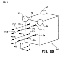
一実施の形態では、前記3つの入射測定ビームの各々は、それに関連する入射基準ビームにほぼ平行である。
Claims (15)
- リソグラフィシステムの第1の鏡と第2の鏡との間の相対的な変位を測定する方法であって、
前記第2の鏡は、前記リソグラフィシステムの露光ツールに接続されており、前記第1の鏡は、前記リソグラフィシステムによって露光されるターゲットに接続されており、
前記第1の鏡は、前記第2の鏡に対して移動可能であり、
この方法は、微分干渉計モジュールを使用することにより実行され、次の工程、
a)3つのコヒーレントビームを発生させる工程と、
b)前記3つのコヒーレントビームを、ユニタリビームスプリッタを使用して、3つの測定ビーム及び関連する基準ビームの対に分割する工程とを具備し、
前記発生させる工程は、前記分割する工程の前に行われ、
この方法は、さらに、
c)前記分割する工程の後に、前記3つの測定ビームが非同一平面上にあるように、前記3つの測定ビームを、前記3つの測定ビームを反射させる前記第1の鏡に入射するように向ける工程、及び、前記3つの基準ビームが非同一平面上にあるように、前記3つの基準ビームを、前記3つの基準ビームを反射させる前記第2の鏡に入射するように向ける工程と、ここで、前記第1の鏡及び前記第2の鏡にそれぞれ入射する前記3つの測定ビームと前記3つの基準ビームは、すべてが互いに平行であり、
d)3つの結合ビームを与えるために、前記3つの反射された測定ビームをこれらの3つの関連する反射された基準ビームと結合させる工程と、ここで、各結合されるビームは、1つの反射された測定ビームと1つの反射された基準ビームとの結合であり、
e)前記3つの結合ビームの各々の1つを、各々が結合されたビームを前記第2の鏡に対する前記第1の鏡の位置と向きとの少なくとも一方を表す信号に変換するように構成された対応するビーム受光器に投影する工程と、を具備する方法であって、
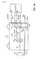
前記微分干渉計モジュールは、前記3つのコヒーレントビーム(b1,b2,b3)を発生させるように構成されたビーム源(32,33,34)と、
前記3つのコヒーレントビームを測定ビーム(mb1,mb2,mb3)と関連する基準ビーム(rb1,rb2,rb3)の各対に分割するように構成されたユニタリビームスプリッタ(42)と、
前記3つの反射された測定ビームと関連する3つの反射された基準ビームとを結合し、対応する3つの結合ビーム(cb1,cb2,cb3)と、前記3つの結合ビームのそれぞれを受光する3つのビーム受光器(51,52,53)とを備える、方法。 - 前記工程d)において、前記3つの結合ビームを与えるためにユニタリビームコンバイナが使用される請求項1に記載の方法。
- 前記3つのコヒーレントビームは、単一のビームから発生される請求項1又は2に記載の方法。
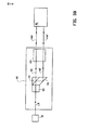
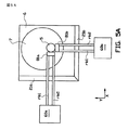
- フレームと、
前記フレームに装着され、第2の鏡が設けられた、ターゲット上にパターンを投影する鏡筒と、
前記鏡筒に対して前記ターゲットを移動させ、第1の鏡が設けられたターゲットキャリアと、
前記鏡筒に対して前記ターゲットキャリアの変位を表す少なくとも1つの信号を発生させ、各々が、3つのコヒーレントビームを発生させるように構成されたビーム源を有する少なくとも1つの微分干渉計モジュールとを具備するリソグラフィシステムであって、
前記少なくとも1つの微分干渉計モジュールの各々は、さらに、
前記3つのコヒーレントビームを受光し、前記3つのコヒーレントビームを3つの測定ビーム及び関連する基準ビームのそれぞれの対に分割するように構成され、前記3つのコヒーレントビームは、前記3つのコヒーレントビームがそれぞれのビーム対に分割される前に発生され、前記3つの測定ビームは、前記第1の鏡に入射して反射するように向けられ、前記3つの基準ビームは、前記第2の鏡に入射して反射するように向けられるビームスプリッタユニットであって、前記3つのコヒーレントビームを、前記3つの測定ビームと前記3つの基準ビームに分割するための単一のビームスプリッタを備える、ビームスプリッタユニットと、
3つの反射された測定ビーム及びこれらに関連する3つの反射された基準ビームを3つの結合ビームへと結合させるための少なくとも1つのビームコンバイナであって、各結合されたビームは、1つの反射された測定ビームと1つの反射された基準ビームとの結合であるビームコンバイナと、
3つのビーム受光器とを有し、前記3つの結合ビームの各々が対応するビーム受光器に投影される、リソグラフィシステム。 - 前記ビームスプリッタユニットは、前記3つのビームを前記3つの測定ビーム/基準ビームの対に分割するための単一のビームスプリッタを有する請求項4に記載のリソグラフィシステム。
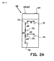
- 前記微分干渉計モジュールは、前記微分干渉計モジュールから前記第1の鏡へと前記3つの測定ビームを非同一平面に照射するように配置され、さらに、前記微分干渉計モジュールから前記第2の鏡へと前記基準ビームを非同一平面に照射するように配置されている請求項4又は5に記載のリソグラフィシステム。
- 前記ビーム受光器は、前記微分干渉計モジュールから出る光ファイバのファイバ端を有する請求項4ないし6のいずれか1項に記載のリソグラフィシステム。
- 前記少なくとも1つの干渉計モジュールは、キネマティックマウントによって前記フレームに装着されている請求項4ないし7のいずれか1項に記載のリソグラフィシステム。
- 前記微分干渉計モジュールは、第1の方向に沿った前記ターゲットキャリアの変位を測定するための第1の微分干渉計モジュールであり、
さらに、前記第1の方向に垂直な第2の方向に沿った前記ターゲットキャリアの変位を測定するための第2の微分干渉計モジュールを具備し、
前記第1及び第2の方向は、前記ターゲットキャリアに対する移動の平面を規定し、
前記第1の微分干渉計モジュールは、さらに、前記第2の方向に平行な軸に沿った回転を表す信号を与えるように構成され、
前記第2の微分干渉計モジュールは、さらに、前記第1の方向に平行な軸に沿った回転を表す信号を与えるように構成されている請求項4ないし8のいずれか1項に記載のリソグラフィシステム。 - 3つのコヒーレントビームを与えるように構成されたビーム源と、
前記3つのコヒーレントビームを受光して、前記3つのコヒーレントビームを測定ビーム及び関連する基準ビームのそれぞれの対に分割するように構成され、前記3つのコヒーレントビームは、前記3つのコヒーレントビームがそれぞれのビーム対に分割される前に発生され、分割された後に、前記3つの測定ビームは、第1の鏡に入射するように向けられ、前記3つの基準ビームは、前記第1の鏡に対して移動可能な第2の鏡に入射するように向けられるビームスプリッタユニットであって、前記3つのコヒーレントビームを、測定ビームと基準ビームとの対のそれぞれに分割するための単一のビームスプリッタを備えた、ビームスプリッタユニットと、
各反射された測定ビーム及びこれらに関連する反射された基準ビームを結合ビームへと結合させるための少なくとも1つのビームコンバイナであって、3つの結合されたビームを形成し、各結合ビームは、1つの反射された測定ビームと1つの反射された基準ビームとの結合であるビームコンバイナと、
3つのビーム受光器とを具備し、各結合ビームが、前記3つのビーム受光器の対応する1つに投影される、微分干渉計モジュール。 - 前記ビームスプリッタユニットは、前記3つのビームを3つの測定ビーム/基準ビームの対に分割するための単一のビームスプリッタを有する請求項10に記載の微分干渉計モジュール。
- 前記3つのビーム受光器の各々は、対応する結合ビームの強度を検出するための強度検出器を有する請求項10又は11に記載の微分干渉計モジュール。
- 前記ビームスプリッタユニットは、前記3つの測定ビームを非同一平面に照射するようにと、前記3つの基準ビームを非同一平面に照射するようにとの少なくとも一方であるように配置されている請求項10ないし12のいずれか1項に記載の微分干渉計モジュール。
- モジュールの内部は、固体材料、好ましくは、硬化エポキシ樹脂で実質的に充填されている請求項10ないし13のいずれか1項に記載の微分干渉計モジュール。
- 前記ビームスプリッタ及び前記ビームコンバイナは、単一の統合ユニットに含まれる請求項10ないし14のいずれか1項に記載の微分干渉計モジュール。
Applications Claiming Priority (3)
| Application Number | Priority Date | Filing Date | Title |
|---|---|---|---|
| NL2006496 | 2011-03-30 | ||
| NL2006496 | 2011-03-30 | ||
| PCT/NL2012/050209 WO2012134290A1 (en) | 2011-03-30 | 2012-03-30 | Lithography system with differential interferometer module |
Publications (2)
| Publication Number | Publication Date |
|---|---|
| JP2014515186A JP2014515186A (ja) | 2014-06-26 |
| JP5985605B2 true JP5985605B2 (ja) | 2016-09-06 |
Family
ID=45930961
Family Applications (3)
| Application Number | Title | Priority Date | Filing Date |
|---|---|---|---|
| JP2014502501A Withdrawn JP2014509750A (ja) | 2011-03-30 | 2012-03-30 | 露光ツール用干渉計モジュールのアライメント |
| JP2014502500A Active JP5985605B2 (ja) | 2011-03-30 | 2012-03-30 | 微分干渉計モジュールを備えたリソグラフィシステム |
| JP2017078979A Active JP6339262B2 (ja) | 2011-03-30 | 2017-04-12 | 露光ツール用干渉計モジュールのアライメント |
Family Applications Before (1)
| Application Number | Title | Priority Date | Filing Date |
|---|---|---|---|
| JP2014502501A Withdrawn JP2014509750A (ja) | 2011-03-30 | 2012-03-30 | 露光ツール用干渉計モジュールのアライメント |
Family Applications After (1)
| Application Number | Title | Priority Date | Filing Date |
|---|---|---|---|
| JP2017078979A Active JP6339262B2 (ja) | 2011-03-30 | 2017-04-12 | 露光ツール用干渉計モジュールのアライメント |
Country Status (8)
| Country | Link |
|---|---|
| US (5) | US9678443B2 (ja) |
| EP (3) | EP2691734B1 (ja) |
| JP (3) | JP2014509750A (ja) |
| KR (2) | KR101955561B1 (ja) |
| CN (5) | CN202793314U (ja) |
| RU (1) | RU2612361C2 (ja) |
| TW (3) | TWI566052B (ja) |
| WO (3) | WO2012134290A1 (ja) |
Families Citing this family (28)
| Publication number | Priority date | Publication date | Assignee | Title |
|---|---|---|---|---|
| CN202793314U (zh) | 2011-03-30 | 2013-03-13 | 迈普尔平版印刷Ip有限公司 | 干涉仪模块和光刻系统 |
| JP6181189B2 (ja) | 2012-09-27 | 2017-08-16 | マッパー・リソグラフィー・アイピー・ビー.ブイ. | 多軸微分干渉計 |
| JP6170694B2 (ja) * | 2013-03-06 | 2017-07-26 | 株式会社荏原製作所 | 測長計の設置構造 |
| CN103257402B (zh) * | 2013-04-23 | 2015-08-12 | 青岛海信宽带多媒体技术有限公司 | 光混合器以及应用光混合器进行信号解调的方法 |
| KR102238107B1 (ko) * | 2014-05-22 | 2021-04-12 | 삼성전자주식회사 | 계측 시스템 및 계측 방법 |
| US9874435B2 (en) * | 2014-05-22 | 2018-01-23 | Samsung Electronics Co., Ltd. | Measuring system and measuring method |
| JP5839759B1 (ja) | 2015-07-30 | 2016-01-06 | 浜松ホトニクス株式会社 | 光干渉計 |
| US10272851B2 (en) * | 2015-10-08 | 2019-04-30 | Toyota Motor Engineering & Manufacturing North America, Inc. | Vehicle emblem alignment and installation tools and methods of use |
| CN106931878A (zh) * | 2015-12-31 | 2017-07-07 | 上海微电子装备有限公司 | 一种干涉仪测量装置及其控制方法 |
| CN107024176A (zh) * | 2016-02-01 | 2017-08-08 | 上海微电子装备有限公司 | 基于衍射光栅的位移测量系统及方法 |
| US10976155B2 (en) * | 2016-09-27 | 2021-04-13 | Intuitive Surgical Operations, Inc. | Micro optic assemblies and optical interrogation systems |
| US10712775B2 (en) * | 2016-12-06 | 2020-07-14 | Facebook Technologies, Llc | Dichroic combiner backlight used in a head mounted display |
| DE102017003084B4 (de) * | 2017-03-31 | 2025-07-17 | Just Vacuum Gmbh | System zum Messen von Längenänderungen im Vakuum |
| WO2019009402A1 (ja) | 2017-07-06 | 2019-01-10 | 浜松ホトニクス株式会社 | 光学デバイス |
| CN107328355B (zh) * | 2017-09-01 | 2023-06-23 | 中科酷原科技(武汉)有限公司 | 用于冷原子干涉仪的集成化光学系统 |
| JP7200234B2 (ja) * | 2017-10-04 | 2023-01-06 | エーエスエムエル ネザーランズ ビー.ブイ. | 干渉計ステージ位置決めデバイス |
| CN108627996B (zh) * | 2018-05-07 | 2020-12-08 | 西安应用光学研究所 | 一种基于双层透光框架的变间隙fp干涉仪装调机构和方法 |
| CN109520428B (zh) * | 2018-11-09 | 2020-01-31 | 中国科学院长春光学精密机械与物理研究所 | 一种位移测量光学系统 |
| KR102125624B1 (ko) * | 2018-11-22 | 2020-07-07 | 전북대학교산학협력단 | 핸드헬드형 분광타원편광계측장치 및 이를 이용한 분광타원편광 파라미터 측정방법 |
| US11698526B2 (en) * | 2019-02-08 | 2023-07-11 | The Charles Stark Draper Laboratory, Inc. | Multi-channel optical system |
| CN109975727B (zh) * | 2019-03-04 | 2020-03-27 | 中国科学技术大学 | 纳米级磁共振扫描成像设备以及方法 |
| CN113939770B (zh) * | 2019-05-30 | 2024-10-11 | Asml控股股份有限公司 | 自参考干涉仪和双重自参考干涉仪装置 |
| CN112113509B (zh) * | 2019-06-20 | 2022-06-17 | 上海微电子装备(集团)股份有限公司 | 龙门式测量装置及龙门式测量方法 |
| CN110806680B (zh) | 2019-10-31 | 2020-11-24 | 清华大学 | 激光干涉光刻系统 |
| CN111045070B (zh) * | 2019-11-26 | 2021-11-30 | 浙江大学 | 一种基于差分干涉仪测量被捕获冷原子的系统及方法 |
| CN110927880B (zh) * | 2019-11-28 | 2021-06-18 | 中国科学院微电子研究所 | 高稳定偏振保持合束装置及方法 |
| US11761750B1 (en) | 2022-02-25 | 2023-09-19 | Utah State University Space Dynamics Laboratory | Multi-environment Rayleigh interferometer |
| EP4647841A1 (en) * | 2024-05-07 | 2025-11-12 | Mycronic AB | Substrate pattern system with sensor heads emitting laser beams for stage position measurement |
Family Cites Families (82)
| Publication number | Priority date | Publication date | Assignee | Title |
|---|---|---|---|---|
| US4504147A (en) | 1981-07-28 | 1985-03-12 | Huang Cheng Chung | Angular alignment sensor |
| DE3262679D1 (en) | 1981-09-03 | 1985-04-25 | Bbc Brown Boveri & Cie | Process for manufacturing an article from a heat-resisting alloy |
| US4528490A (en) * | 1982-08-11 | 1985-07-09 | Hughes Aircraft Company | Two axis drive for stage |
| JPS60203804A (ja) | 1984-03-29 | 1985-10-15 | Mitsubishi Heavy Ind Ltd | 真直度測定装置 |
| US4891526A (en) | 1986-12-29 | 1990-01-02 | Hughes Aircraft Company | X-Y-θ-Z positioning stage |
| JPH01184402A (ja) * | 1988-01-18 | 1989-07-24 | Hitachi Electron Eng Co Ltd | 光学式変位測定方法および測定装置 |
| NL9100215A (nl) * | 1991-02-07 | 1992-09-01 | Asm Lithography Bv | Inrichting voor het repeterend afbeelden van een maskerpatroon op een substraat. |
| RU2047085C1 (ru) | 1992-06-30 | 1995-10-27 | Владимир Николаевич Давыдов | Интерферометр для измерения перемещений двухкоординатного стола |
| US5719702A (en) | 1993-08-03 | 1998-02-17 | The United States Of America As Represented By The United States Department Of Energy | Polarization-balanced beamsplitter |
| JP3367209B2 (ja) * | 1994-05-30 | 2003-01-14 | 株式会社ニコン | 干渉計 |
| US6122036A (en) | 1993-10-21 | 2000-09-19 | Nikon Corporation | Projection exposure apparatus and method |
| JP3413945B2 (ja) | 1994-01-28 | 2003-06-09 | 株式会社ニコン | 縞計数変位干渉計 |
| JPH08210814A (ja) | 1994-10-12 | 1996-08-20 | Canon Inc | 光学式変位測定装置 |
| JP3315540B2 (ja) | 1994-10-28 | 2002-08-19 | キヤノン株式会社 | 位置計測装置、位置合わせ装置、露光装置およびデバイスの製造方法 |
| JP3739121B2 (ja) | 1995-10-30 | 2006-01-25 | 株式会社ソキア | レーザ測長機 |
| DE69705779T2 (de) * | 1996-03-06 | 2002-05-23 | Asm Lithography B.V., Veldhoven | Differential-interferometer-system und lithographischer "step and scan" apparat ausgestattet mit diesem system |
| US6020963A (en) | 1996-06-04 | 2000-02-01 | Northeastern University | Optical quadrature Interferometer |
| US5880838A (en) | 1996-06-05 | 1999-03-09 | California Institute Of California | System and method for optically measuring a structure |
| US6507326B2 (en) | 1996-07-10 | 2003-01-14 | Nikon Corporation | Color-projection apparatus operable to project a high-contrast image with minimal change in the state or phase of polarization of light flux |
| JP2879325B2 (ja) | 1996-07-29 | 1999-04-05 | 新菱冷熱工業株式会社 | レーザ光を用いた配管組立治具 |
| JP3832681B2 (ja) * | 1997-03-19 | 2006-10-11 | 株式会社ニコン | ステージ装置及び該装置を備えた露光装置 |
| US5949546A (en) | 1997-05-14 | 1999-09-07 | Ahead Optoelectronics, Inc. | Interference apparatus for measuring absolute and differential motions of same or different testing surface |
| KR100228285B1 (ko) | 1997-07-23 | 1999-11-01 | 윤종용 | 액정 표시 장치의 액정 물질 주입 장치 및 그 방법 |
| AU8746998A (en) * | 1997-08-19 | 1999-03-08 | Nikon Corporation | Object observation device and object observation method |
| IL135139A0 (en) | 1997-09-19 | 2001-05-20 | Nikon Corp | Stage apparatus, scanning type exposure apparatus, and device produced with the same |
| US6020964A (en) | 1997-12-02 | 2000-02-01 | Asm Lithography B.V. | Interferometer system and lithograph apparatus including an interferometer system |
| JPH11265847A (ja) | 1998-01-16 | 1999-09-28 | Canon Inc | 位置検出方法及び位置検出装置 |
| JPH11281319A (ja) | 1998-03-30 | 1999-10-15 | Sumitomo Heavy Ind Ltd | 光学素子の位置設定装置、及び光学素子の位置設定方法 |
| US6765217B1 (en) * | 1998-04-28 | 2004-07-20 | Nikon Corporation | Charged-particle-beam mapping projection-optical systems and methods for adjusting same |
| JP4109765B2 (ja) | 1998-09-14 | 2008-07-02 | キヤノン株式会社 | 結像性能評価方法 |
| US7139080B2 (en) * | 1998-09-18 | 2006-11-21 | Zygo Corporation | Interferometry systems involving a dynamic beam-steering assembly |
| US6181420B1 (en) * | 1998-10-06 | 2001-01-30 | Zygo Corporation | Interferometry system having reduced cyclic errors |
| WO2000022376A1 (en) * | 1998-10-14 | 2000-04-20 | Nikon Corporation | Shape measuring method and shape measuring device, position control method, stage device, exposure apparatus and method for producing exposure apparatus, and device and method for manufacturing device |
| JP3796363B2 (ja) | 1998-10-30 | 2006-07-12 | キヤノン株式会社 | 位置検出装置及びそれを用いた露光装置 |
| US6550919B1 (en) | 1999-03-26 | 2003-04-22 | Unaxis Balzers Aktiengesellschaft | Spectral light division and recombination configuration as well as process for the spectrally selective modulation of light |
| US6201609B1 (en) * | 1999-08-27 | 2001-03-13 | Zygo Corporation | Interferometers utilizing polarization preserving optical systems |
| CN1117963C (zh) * | 2000-07-07 | 2003-08-13 | 清华大学 | 利用合成波长法实现纳米测量的方法 |
| JP2002141393A (ja) * | 2000-07-18 | 2002-05-17 | Nikon Corp | 干渉計ボックス |
| US6727992B2 (en) * | 2001-07-06 | 2004-04-27 | Zygo Corporation | Method and apparatus to reduce effects of sheared wavefronts on interferometric phase measurements |
| WO2003033199A1 (en) | 2001-10-19 | 2003-04-24 | U.C. Laser Ltd. | Method for improved wafer alignment |
| WO2003062926A2 (de) | 2002-01-24 | 2003-07-31 | Jenoptik Laser, Optik, Systeme Gmbh | Verfahren zum aufbau eines optischen strahlführungssystems |
| US6757066B2 (en) | 2002-01-28 | 2004-06-29 | Zygo Corporation | Multiple degree of freedom interferometer |
| TWI277720B (en) * | 2002-01-28 | 2007-04-01 | Zygo Corp | Multi-axis interferometer apparatus and method, lithography apparatus and method using same, and beam writing system and method using same |
| DE10206061A1 (de) | 2002-02-08 | 2003-09-04 | Carl Zeiss Semiconductor Mfg S | Polarisationsoptimiertes Beleuchtungssystem |
| US7057739B2 (en) * | 2002-02-12 | 2006-06-06 | Zygo Corporation | Separated beam multiple degree of freedom interferometer |
| GB0222970D0 (en) * | 2002-10-04 | 2002-11-13 | Renishaw Plc | Vacuum compatible laser interferometer |
| EP1583934A1 (en) * | 2002-12-12 | 2005-10-12 | Zygo Corporation | In-process correction of stage mirror deformations during a photolithography exposure cycle |
| CN1252444C (zh) * | 2002-12-24 | 2006-04-19 | 中国航空工业总公司第三○四研究所 | 一种实现阿贝误差实时补偿的激光干涉测长系统 |
| EP1590625A4 (en) | 2003-01-15 | 2007-08-01 | Inlight Solutions Inc | Interferometer |
| JP2004228382A (ja) | 2003-01-23 | 2004-08-12 | Nikon Corp | 露光装置 |
| US7224466B2 (en) * | 2003-02-05 | 2007-05-29 | Agilent Technologies, Inc. | Compact multi-axis interferometer |
| CN1227520C (zh) * | 2003-05-14 | 2005-11-16 | 安徽大学 | 远距离散射物微振动信号测量和保真拾取干涉仪 |
| JP2005057222A (ja) | 2003-08-07 | 2005-03-03 | Canon Inc | マーク検出装置、マーク検出方法、マーク検出プログラム、露光装置、デバイスの製造方法、及び、デバイス |
| WO2005047974A2 (en) * | 2003-11-10 | 2005-05-26 | Zygo Corporation | Measurement and compensation of errors in interferometers |
| US7443511B2 (en) * | 2003-11-25 | 2008-10-28 | Asml Netherlands B.V. | Integrated plane mirror and differential plane mirror interferometer system |
| DE102004023030B4 (de) | 2004-05-06 | 2012-12-27 | SIOS Meßtechnik GmbH | Mehrfachstrahlteiler |
| JP2005345329A (ja) * | 2004-06-04 | 2005-12-15 | Tokyo Seimitsu Co Ltd | 測長用レーザ干渉計 |
| US7212290B2 (en) | 2004-07-28 | 2007-05-01 | Agilent Technologies, Inc. | Differential interferometers creating desired beam patterns |
| US20080068568A1 (en) * | 2004-09-30 | 2008-03-20 | Nikon Corporation | Projection Optical Device And Exposure Apparatus |
| JP4465451B2 (ja) | 2004-12-15 | 2010-05-19 | 独立行政法人産業技術総合研究所 | 光干渉計の周期誤差低減方法および装置 |
| US7298492B2 (en) | 2004-12-29 | 2007-11-20 | Honeywell International Inc. | Method and system for on-line measurement of thickness and birefringence of thin plastic films |
| JP5149486B2 (ja) | 2005-05-18 | 2013-02-20 | 株式会社ミツトヨ | 干渉計、形状測定方法 |
| US7355719B2 (en) | 2005-08-16 | 2008-04-08 | Agilent Technologies, Inc. | Interferometer for measuring perpendicular translations |
| US7362446B2 (en) * | 2005-09-15 | 2008-04-22 | Asml Netherlands B.V. | Position measurement unit, measurement system and lithographic apparatus comprising such position measurement unit |
| US7397039B2 (en) | 2005-09-30 | 2008-07-08 | Applied Materials, Inc. | Real-time compensation of mechanical position error in pattern generation or imaging applications |
| JP4631655B2 (ja) | 2005-10-31 | 2011-02-16 | セイコーエプソン株式会社 | 光伝送モジュール、光伝送モジュールの製造方法、光インターコネクション回路及び電子機器 |
| US7379187B2 (en) * | 2006-03-31 | 2008-05-27 | Mitutoyo Corporation | Detector configuration for interferometric distance measurement |
| JP4191201B2 (ja) | 2006-04-25 | 2008-12-03 | アンリツ株式会社 | 三次元形状測定装置 |
| DE102007017630B4 (de) | 2006-05-16 | 2009-08-20 | Vistec Semiconductor Systems Gmbh | Verfahren zum Steigern der Messgenauigkeit beim Bestimmen der Koordinaten von Strukturen auf einem Substrat |
| JP5613893B2 (ja) | 2006-05-22 | 2014-10-29 | 株式会社ブイ・テクノロジー | 作業装置におけるテーブル位置決め装置および位置決め方法。 |
| KR20090081029A (ko) | 2006-12-08 | 2009-07-27 | 캐논 가부시끼가이샤 | 노광장치 |
| JP4264667B2 (ja) | 2007-02-16 | 2009-05-20 | ソニー株式会社 | 振動検出装置 |
| JP5523664B2 (ja) | 2007-11-06 | 2014-06-18 | 株式会社ミツトヨ | 干渉計 |
| US20090135430A1 (en) | 2007-11-26 | 2009-05-28 | Miao Zhu | Systems and Methods for Reducing Nonlinearity in an Interferometer |
| US8711327B2 (en) | 2007-12-14 | 2014-04-29 | Nikon Corporation | Exposure apparatus, exposure method, and device manufacturing method |
| US7897942B1 (en) | 2007-12-20 | 2011-03-01 | Kla-Tencor Corporation | Dynamic tracking of wafer motion and distortion during lithography |
| DE102008004762A1 (de) * | 2008-01-16 | 2009-07-30 | Carl Zeiss Smt Ag | Projektionsbelichtungsanlage für die Mikrolithographie mit einer Messeinrichtung |
| TW200951640A (en) * | 2008-04-30 | 2009-12-16 | Nikon Corp | Exposure apparatus, exposure method, and device manufacturing method |
| WO2010004900A1 (ja) | 2008-07-09 | 2010-01-14 | 株式会社ニコン | 位置計測方法、並びに露光方法及び装置 |
| CN102187424B (zh) | 2008-08-18 | 2013-07-17 | 迈普尔平版印刷Ip有限公司 | 带电粒子束光刻系统以及目标定位装置 |
| US8462349B1 (en) | 2010-07-20 | 2013-06-11 | Science Applications International Corporation | System and method for a self-referencing interferometer |
| CN202793314U (zh) | 2011-03-30 | 2013-03-13 | 迈普尔平版印刷Ip有限公司 | 干涉仪模块和光刻系统 |
-
2012
- 2012-03-30 CN CN2012201314341U patent/CN202793314U/zh not_active Expired - Lifetime
- 2012-03-30 CN CN201710222191.XA patent/CN107036528B/zh active Active
- 2012-03-30 WO PCT/NL2012/050209 patent/WO2012134290A1/en not_active Ceased
- 2012-03-30 TW TW101111337A patent/TWI566052B/zh active
- 2012-03-30 TW TW101111339A patent/TWI624733B/zh active
- 2012-03-30 WO PCT/NL2012/050211 patent/WO2012134292A1/en not_active Ceased
- 2012-03-30 TW TW101111338A patent/TW201243278A/zh unknown
- 2012-03-30 WO PCT/NL2012/050210 patent/WO2012134291A1/en not_active Ceased
- 2012-03-30 JP JP2014502501A patent/JP2014509750A/ja not_active Withdrawn
- 2012-03-30 US US13/436,736 patent/US9678443B2/en active Active
- 2012-03-30 EP EP12712417.0A patent/EP2691734B1/en active Active
- 2012-03-30 CN CN2012201314981U patent/CN202793315U/zh not_active Expired - Lifetime
- 2012-03-30 CN CN201210091620.1A patent/CN102735170B/zh active Active
- 2012-03-30 EP EP12712415.4A patent/EP2691812B1/en active Active
- 2012-03-30 RU RU2013148110A patent/RU2612361C2/ru active
- 2012-03-30 US US13/436,738 patent/US9069265B2/en active Active
- 2012-03-30 CN CN201210091968.0A patent/CN102735163B/zh active Active
- 2012-03-30 US US13/436,741 patent/US9261800B2/en active Active
- 2012-03-30 KR KR1020137028680A patent/KR101955561B1/ko active Active
- 2012-03-30 JP JP2014502500A patent/JP5985605B2/ja active Active
- 2012-03-30 KR KR1020137028682A patent/KR101804610B1/ko active Active
- 2012-03-30 EP EP12712416.2A patent/EP2691733B1/en active Active
-
2015
- 2015-05-19 US US14/716,801 patent/US9690215B2/en active Active
-
2017
- 2017-04-12 JP JP2017078979A patent/JP6339262B2/ja active Active
- 2017-06-12 US US15/620,699 patent/US20170277043A1/en not_active Abandoned
Also Published As
Similar Documents
| Publication | Publication Date | Title |
|---|---|---|
| JP5985605B2 (ja) | 微分干渉計モジュールを備えたリソグラフィシステム | |
| US9395636B2 (en) | Lithography system for processing a target, such as a wafer, and a method for operating a lithography system for processing a target, such as a wafer | |
| JP6219320B2 (ja) | ウェーハなどのターゲットを処理するためのリソグラフィシステム及び方法 | |
| US9551563B2 (en) | Multi-axis differential interferometer | |
| JP2009002673A (ja) | 干渉計のアライメント装置 | |
| JP2005345356A (ja) | 平面度測定における取付位置の測定方法並びにその装置 |
Legal Events
| Date | Code | Title | Description |
|---|---|---|---|
| A621 | Written request for application examination |
Free format text: JAPANESE INTERMEDIATE CODE: A621 Effective date: 20150325 |
|
| A131 | Notification of reasons for refusal |
Free format text: JAPANESE INTERMEDIATE CODE: A131 Effective date: 20160105 |
|
| A521 | Request for written amendment filed |
Free format text: JAPANESE INTERMEDIATE CODE: A523 Effective date: 20160405 |
|
| TRDD | Decision of grant or rejection written | ||
| A01 | Written decision to grant a patent or to grant a registration (utility model) |
Free format text: JAPANESE INTERMEDIATE CODE: A01 Effective date: 20160712 |
|
| A61 | First payment of annual fees (during grant procedure) |
Free format text: JAPANESE INTERMEDIATE CODE: A61 Effective date: 20160803 |
|
| R150 | Certificate of patent or registration of utility model |
Ref document number: 5985605 Country of ref document: JP Free format text: JAPANESE INTERMEDIATE CODE: R150 |
|
| S111 | Request for change of ownership or part of ownership |
Free format text: JAPANESE INTERMEDIATE CODE: R313113 |
|
| R350 | Written notification of registration of transfer |
Free format text: JAPANESE INTERMEDIATE CODE: R350 |
|
| RD02 | Notification of acceptance of power of attorney |
Free format text: JAPANESE INTERMEDIATE CODE: R3D02 |
|
| R250 | Receipt of annual fees |
Free format text: JAPANESE INTERMEDIATE CODE: R250 |
|
| R250 | Receipt of annual fees |
Free format text: JAPANESE INTERMEDIATE CODE: R250 |
|
| R250 | Receipt of annual fees |
Free format text: JAPANESE INTERMEDIATE CODE: R250 |
|
| R250 | Receipt of annual fees |
Free format text: JAPANESE INTERMEDIATE CODE: R250 |
|
| R250 | Receipt of annual fees |
Free format text: JAPANESE INTERMEDIATE CODE: R250 |
|
| R250 | Receipt of annual fees |
Free format text: JAPANESE INTERMEDIATE CODE: R250 |
|
| R250 | Receipt of annual fees |
Free format text: JAPANESE INTERMEDIATE CODE: R250 |