JP6060652B2 - 太陽電池及びその製造方法 - Google Patents
太陽電池及びその製造方法 Download PDFInfo
- Publication number
- JP6060652B2 JP6060652B2 JP2012259941A JP2012259941A JP6060652B2 JP 6060652 B2 JP6060652 B2 JP 6060652B2 JP 2012259941 A JP2012259941 A JP 2012259941A JP 2012259941 A JP2012259941 A JP 2012259941A JP 6060652 B2 JP6060652 B2 JP 6060652B2
- Authority
- JP
- Japan
- Prior art keywords
- layer
- type
- type gan
- solar cell
- ingan
- Prior art date
- Legal status (The legal status is an assumption and is not a legal conclusion. Google has not performed a legal analysis and makes no representation as to the accuracy of the status listed.)
- Expired - Fee Related
Links
Images




Classifications
-
- Y—GENERAL TAGGING OF NEW TECHNOLOGICAL DEVELOPMENTS; GENERAL TAGGING OF CROSS-SECTIONAL TECHNOLOGIES SPANNING OVER SEVERAL SECTIONS OF THE IPC; TECHNICAL SUBJECTS COVERED BY FORMER USPC CROSS-REFERENCE ART COLLECTIONS [XRACs] AND DIGESTS
- Y02—TECHNOLOGIES OR APPLICATIONS FOR MITIGATION OR ADAPTATION AGAINST CLIMATE CHANGE
- Y02E—REDUCTION OF GREENHOUSE GAS [GHG] EMISSIONS, RELATED TO ENERGY GENERATION, TRANSMISSION OR DISTRIBUTION
- Y02E10/00—Energy generation through renewable energy sources
- Y02E10/50—Photovoltaic [PV] energy
Landscapes
- Photovoltaic Devices (AREA)
Description
また、実施形態の他の観点によれば、p型の半導体基板と、前記半導体基板上に形成されたp型GaN層と、前記p型GaN層上に形成されたInGaN光吸収層と、前記InGaN光吸収層上に形成されたn型GaN層とを有する柱状構造体と、前記半導体基板と前記p型GaN層との間に形成され、金属的伝導性を有するp型GaP層のp型半導体層とを有することを特徴とする太陽電池が提供される。
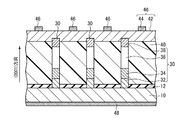
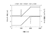
第1実施形態による太陽電池及びその製造方法について図1乃至図4を用いて説明する。
d=λ/n=400/3.2=125(nm)
となる。
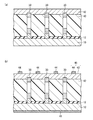
第2実施形態による太陽電池及びその製造方法について図5乃至図7を用いて説明する。図1乃至図4に示す第1実施形態による太陽電池及びその製造方法と同様の構成要素には同一の符号を付し説明を省略し又は簡潔にする。
上記実施形態に限らず種々の変形が可能である。
12…絶縁膜
14…開口部
30…柱状構造体
32…p型半導体層
34…p型GaN層
36…i型InGaN層
38…n型GaN層
40…樹脂層
42…透明電極
44…金属グリッド電極
46…n側電極
48…p側電極
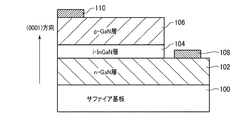
100…サファイア基板
102…n型GaN層
104…i型InGaN層
106…p型GaN層
108…n側電極
110…p側電極
Claims (8)
- p型の半導体基板と、
前記半導体基板上に形成されたp型GaN層と、前記p型GaN層上に形成されたInGaN光吸収層と、前記InGaN光吸収層上に形成されたn型GaN層とを有する柱状構造体と、
前記半導体基板と前記p型GaN層との間に形成され、金属的伝導性を有するp型GaAs層又はp型Si層のp型半導体層と
を有することを特徴とする太陽電池。 - p型の半導体基板と、
前記半導体基板上に形成されたp型GaN層と、前記p型GaN層上に形成されたInGaN光吸収層と、前記InGaN光吸収層上に形成されたn型GaN層とを有する柱状構造体と、
前記半導体基板と前記p型GaN層との間に形成され、金属的伝導性を有するp型GaP層のp型半導体層と
を有することを特徴とする太陽電池。 - 請求項1又は2記載の太陽電池において、
前記p型GaN層、前記InGaN光吸収層及び前記n型GaN層は、(0001)方向に配向している
ことを特徴とする太陽電池。 - 請求項1記載の太陽電池において、
前記半導体基板は、GaAs(111)基板である
ことを特徴とする太陽電池。 - 請求項2記載の太陽電池において、
前記半導体基板は、SiC(111)基板である
ことを特徴とする太陽電池。 - 請求項1乃至5のいずれか1項に記載の太陽電池において、
前記柱状構造体の直径は、125nm〜400nmである
ことを特徴とする太陽電池。 - 請求項1乃至6のいずれか1項に記載の太陽電池において、
前記半導体基板に接続されたp側電極と、
前記n型GaN層に接続されたn側電極と
を更に有することを特徴とする太陽電池。 - p型の半導体基板上に、開口部を有するマスク膜を形成する工程と、
前記マスク膜をマスクとして、前記開口部内の前記半導体基板上に、p型GaN層と、InGaN光吸収層と、n型GaN層とを(0001)方向に配向して順次成長し、前記p型GaN層、前記InGaN光吸収層及び前記n型GaN層の積層構造を有する柱状構造体を形成する工程と
を有することを特徴とする太陽電池の製造方法。
Priority Applications (1)
| Application Number | Priority Date | Filing Date | Title |
|---|---|---|---|
| JP2012259941A JP6060652B2 (ja) | 2012-11-28 | 2012-11-28 | 太陽電池及びその製造方法 |
Applications Claiming Priority (1)
| Application Number | Priority Date | Filing Date | Title |
|---|---|---|---|
| JP2012259941A JP6060652B2 (ja) | 2012-11-28 | 2012-11-28 | 太陽電池及びその製造方法 |
Publications (2)
| Publication Number | Publication Date |
|---|---|
| JP2014107441A JP2014107441A (ja) | 2014-06-09 |
| JP6060652B2 true JP6060652B2 (ja) | 2017-01-18 |
Family
ID=51028667
Family Applications (1)
| Application Number | Title | Priority Date | Filing Date |
|---|---|---|---|
| JP2012259941A Expired - Fee Related JP6060652B2 (ja) | 2012-11-28 | 2012-11-28 | 太陽電池及びその製造方法 |
Country Status (1)
| Country | Link |
|---|---|
| JP (1) | JP6060652B2 (ja) |
Cited By (5)
| Publication number | Priority date | Publication date | Assignee | Title |
|---|---|---|---|---|
| US10502435B2 (en) | 2013-09-06 | 2019-12-10 | Zinniatek Limited | Solar thermal roofing system |
| US10858839B2 (en) | 2011-11-30 | 2020-12-08 | Zinniatek Limited | Roofing, cladding or siding product, its manufacture and its use as part of a solar energy recovery system |
| US11011912B2 (en) | 2011-11-30 | 2021-05-18 | Zinniatek Limited | Photovoltaic systems |
| US11408613B2 (en) | 2014-03-07 | 2022-08-09 | Zinniatek Limited | Solar thermal roofing system |
| US11970858B2 (en) | 2017-02-21 | 2024-04-30 | Zinniatek Limited | Substrate having decorated surface and method of production |
Families Citing this family (1)
| Publication number | Priority date | Publication date | Assignee | Title |
|---|---|---|---|---|
| JP6619370B2 (ja) * | 2017-02-13 | 2019-12-11 | 日本電信電話株式会社 | 光反応装置 |
Family Cites Families (15)
| Publication number | Priority date | Publication date | Assignee | Title |
|---|---|---|---|---|
| JP3332127B2 (ja) * | 1995-03-20 | 2002-10-07 | 株式会社東芝 | 半導体素子 |
| JP3955367B2 (ja) * | 1997-09-30 | 2007-08-08 | フィリップス ルミレッズ ライティング カンパニー リミテッド ライアビリティ カンパニー | 光半導体素子およびその製造方法 |
| JP2000277440A (ja) * | 1999-03-25 | 2000-10-06 | Nec Corp | 窒化物系iii−v族化合物半導体結晶膜、窒化物系iii−v族化合物半導体結晶膜をもちいた半導体装置及び窒化物系iii−v族化合物半導体結晶膜をもちいた半導体レーザ |
| JP3702700B2 (ja) * | 1999-03-31 | 2005-10-05 | 豊田合成株式会社 | Iii族窒化物系化合物半導体素子及びその製造方法 |
| JP4104305B2 (ja) * | 2001-08-07 | 2008-06-18 | 三洋電機株式会社 | 窒化物系半導体チップおよび窒化物系半導体基板 |
| JP4118061B2 (ja) * | 2002-02-07 | 2008-07-16 | 三洋電機株式会社 | 半導体の形成方法および半導体素子 |
| JP2003318434A (ja) * | 2002-04-25 | 2003-11-07 | Nichia Chem Ind Ltd | 窒化物半導体受光素子とその製造方法 |
| US20060207647A1 (en) * | 2005-03-16 | 2006-09-21 | General Electric Company | High efficiency inorganic nanorod-enhanced photovoltaic devices |
| JP5324222B2 (ja) * | 2005-08-22 | 2013-10-23 | キュー・ワン・ナノシステムズ・インコーポレイテッド | ナノ構造およびそれを実施する光起電力セル |
| US7629532B2 (en) * | 2006-12-29 | 2009-12-08 | Sundiode, Inc. | Solar cell having active region with nanostructures having energy wells |
| US8183566B2 (en) * | 2007-03-01 | 2012-05-22 | Hewlett-Packard Development Company, L.P. | Hetero-crystalline semiconductor device and method of making same |
| WO2010023921A1 (ja) * | 2008-09-01 | 2010-03-04 | 学校法人上智学院 | 半導体光素子アレイおよびその製造方法 |
| US20100148221A1 (en) * | 2008-11-13 | 2010-06-17 | Zena Technologies, Inc. | Vertical photogate (vpg) pixel structure with nanowires |
| US20110115041A1 (en) * | 2009-11-19 | 2011-05-19 | Zena Technologies, Inc. | Nanowire core-shell light pipes |
| JP2012188294A (ja) * | 2011-03-08 | 2012-10-04 | Tohoku Univ | 半導体装置の製造方法 |
-
2012
- 2012-11-28 JP JP2012259941A patent/JP6060652B2/ja not_active Expired - Fee Related
Cited By (5)
| Publication number | Priority date | Publication date | Assignee | Title |
|---|---|---|---|---|
| US10858839B2 (en) | 2011-11-30 | 2020-12-08 | Zinniatek Limited | Roofing, cladding or siding product, its manufacture and its use as part of a solar energy recovery system |
| US11011912B2 (en) | 2011-11-30 | 2021-05-18 | Zinniatek Limited | Photovoltaic systems |
| US10502435B2 (en) | 2013-09-06 | 2019-12-10 | Zinniatek Limited | Solar thermal roofing system |
| US11408613B2 (en) | 2014-03-07 | 2022-08-09 | Zinniatek Limited | Solar thermal roofing system |
| US11970858B2 (en) | 2017-02-21 | 2024-04-30 | Zinniatek Limited | Substrate having decorated surface and method of production |
Also Published As
| Publication number | Publication date |
|---|---|
| JP2014107441A (ja) | 2014-06-09 |
Similar Documents
| Publication | Publication Date | Title |
|---|---|---|
| US10050166B2 (en) | Silicon heterojunction photovoltaic device with wide band gap emitter | |
| JP3657143B2 (ja) | 太陽電池及びその製造方法 | |
| US8952243B2 (en) | Stacked structure including vertically grown semiconductor, p-n junction device including the stacked structure, and method of manufacturing thereof | |
| CN102456763A (zh) | 包含异质结的光电子器件 | |
| JP6060652B2 (ja) | 太陽電池及びその製造方法 | |
| US20120305059A1 (en) | Photon recycling in an optoelectronic device | |
| US9324911B2 (en) | Methods of fabricating dilute nitride semiconductor materials for use in photoactive devices and related structures | |
| US20160056333A1 (en) | Nitride semiconductor multilayer film reflector and light-emitting device using the same | |
| CN107342535A (zh) | 基于GeSn/SiGeSn材料的应变多量子阱激光器及其制作方法 | |
| JP2010267934A (ja) | 太陽電池およびその製造方法 | |
| CN107546287B (zh) | 一种太阳能电池及其制作方法 | |
| US20180287015A1 (en) | Semiconductor device | |
| JP6335784B2 (ja) | 可変バンドギャップ太陽電池 | |
| TWI496314B (zh) | Compound semiconductor solar cell manufacturing laminated body, compound semiconductor solar cell and manufacturing method thereof | |
| JP5634955B2 (ja) | Iii−v族化合物半導体膜の製造方法および化合物半導体太陽電池の製造方法 | |
| JP2010171374A (ja) | 太陽電池 | |
| CN102738267B (zh) | 具有超晶格结构的太阳能电池及其制备方法 | |
| Yu et al. | Conversion efficiency improvement of InGaN/GaN multiple-quantum-well solar cells with ex situ AlN nucleation layer | |
| CN104617167A (zh) | 形成光伏器件的方法以及光伏器件 | |
| KR101539183B1 (ko) | 하부 폭에 비해 상부 폭이 좁은 다면체, 이의 제조방법, 및 이를 포함하는 광전변환소자 | |
| Zhang et al. | Photovoltaic effects of InGaN/GaN double heterojunctions with p-GaN nanorod arrays | |
| CN111785806A (zh) | 一种太阳能电池以及制作方法 | |
| US10763111B2 (en) | Polyhedron of which upper width is narrower than lower width, manufacturing method therefor, and photoelectric conversion device comprising same | |
| JP2013197485A (ja) | エピタキシャル基板及びこれを用いた半導体素子の製造方法 | |
| JP2013183125A (ja) | 化合物半導体素子エピタキシャル成長基板 |
Legal Events
| Date | Code | Title | Description |
|---|---|---|---|
| A621 | Written request for application examination |
Free format text: JAPANESE INTERMEDIATE CODE: A621 Effective date: 20150706 |
|
| A977 | Report on retrieval |
Free format text: JAPANESE INTERMEDIATE CODE: A971007 Effective date: 20160229 |
|
| A131 | Notification of reasons for refusal |
Free format text: JAPANESE INTERMEDIATE CODE: A131 Effective date: 20160308 |
|
| A521 | Request for written amendment filed |
Free format text: JAPANESE INTERMEDIATE CODE: A523 Effective date: 20160506 |
|
| A131 | Notification of reasons for refusal |
Free format text: JAPANESE INTERMEDIATE CODE: A131 Effective date: 20160719 |
|
| A521 | Request for written amendment filed |
Free format text: JAPANESE INTERMEDIATE CODE: A523 Effective date: 20160906 |
|
| TRDD | Decision of grant or rejection written | ||
| A01 | Written decision to grant a patent or to grant a registration (utility model) |
Free format text: JAPANESE INTERMEDIATE CODE: A01 Effective date: 20161115 |
|
| A61 | First payment of annual fees (during grant procedure) |
Free format text: JAPANESE INTERMEDIATE CODE: A61 Effective date: 20161128 |
|
| R150 | Certificate of patent or registration of utility model |
Ref document number: 6060652 Country of ref document: JP Free format text: JAPANESE INTERMEDIATE CODE: R150 |
|
| LAPS | Cancellation because of no payment of annual fees |