JP6073339B2 - 部品内蔵基板の製造方法及びこれを用いた部品内蔵基板 - Google Patents
部品内蔵基板の製造方法及びこれを用いた部品内蔵基板 Download PDFInfo
- Publication number
- JP6073339B2 JP6073339B2 JP2014535252A JP2014535252A JP6073339B2 JP 6073339 B2 JP6073339 B2 JP 6073339B2 JP 2014535252 A JP2014535252 A JP 2014535252A JP 2014535252 A JP2014535252 A JP 2014535252A JP 6073339 B2 JP6073339 B2 JP 6073339B2
- Authority
- JP
- Japan
- Prior art keywords
- component
- adhesive
- adhesive body
- layer
- metal layer
- Prior art date
- Legal status (The legal status is an assumption and is not a legal conclusion. Google has not performed a legal analysis and makes no representation as to the accuracy of the status listed.)
- Active
Links
Images



Classifications
-
- H—ELECTRICITY
- H10—SEMICONDUCTOR DEVICES; ELECTRIC SOLID-STATE DEVICES NOT OTHERWISE PROVIDED FOR
- H10W—GENERIC PACKAGES, INTERCONNECTIONS, CONNECTORS OR OTHER CONSTRUCTIONAL DETAILS OF DEVICES COVERED BY CLASS H10
- H10W72/00—Interconnections or connectors in packages
- H10W72/071—Connecting or disconnecting
- H10W72/073—Connecting or disconnecting of die-attach connectors
-
- H—ELECTRICITY
- H05—ELECTRIC TECHNIQUES NOT OTHERWISE PROVIDED FOR
- H05K—PRINTED CIRCUITS; CASINGS OR CONSTRUCTIONAL DETAILS OF ELECTRIC APPARATUS; MANUFACTURE OF ASSEMBLAGES OF ELECTRICAL COMPONENTS
- H05K1/00—Printed circuits
- H05K1/18—Printed circuits structurally associated with non-printed electric components
-
- H—ELECTRICITY
- H05—ELECTRIC TECHNIQUES NOT OTHERWISE PROVIDED FOR
- H05K—PRINTED CIRCUITS; CASINGS OR CONSTRUCTIONAL DETAILS OF ELECTRIC APPARATUS; MANUFACTURE OF ASSEMBLAGES OF ELECTRICAL COMPONENTS
- H05K1/00—Printed circuits
- H05K1/18—Printed circuits structurally associated with non-printed electric components
- H05K1/182—Printed circuits structurally associated with non-printed electric components associated with components mounted in printed circuit boards [PCB], e.g. insert-mounted components [IMC]
- H05K1/185—Printed circuits structurally associated with non-printed electric components associated with components mounted in printed circuit boards [PCB], e.g. insert-mounted components [IMC] associated with components encapsulated in the insulating substrate of the PCBs; associated with components incorporated in internal layers of multilayer circuit boards
- H05K1/188—Printed circuits structurally associated with non-printed electric components associated with components mounted in printed circuit boards [PCB], e.g. insert-mounted components [IMC] associated with components encapsulated in the insulating substrate of the PCBs; associated with components incorporated in internal layers of multilayer circuit boards manufactured by mounting on or attaching to a structure having a conductive layer, e.g. a metal foil, such that the terminals of the component are connected to or adjacent to the conductive layer before embedding, and by using the conductive layer, which is patterned after embedding, at least partially for connecting the component
-
- H—ELECTRICITY
- H10—SEMICONDUCTOR DEVICES; ELECTRIC SOLID-STATE DEVICES NOT OTHERWISE PROVIDED FOR
- H10W—GENERIC PACKAGES, INTERCONNECTIONS, CONNECTORS OR OTHER CONSTRUCTIONAL DETAILS OF DEVICES COVERED BY CLASS H10
- H10W20/00—Interconnections in chips, wafers or substrates
- H10W20/01—Manufacture or treatment
- H10W20/031—Manufacture or treatment of conductive parts of the interconnections
- H10W20/056—Manufacture or treatment of conductive parts of the interconnections by filling conductive material into holes, grooves or trenches
-
- H—ELECTRICITY
- H10—SEMICONDUCTOR DEVICES; ELECTRIC SOLID-STATE DEVICES NOT OTHERWISE PROVIDED FOR
- H10W—GENERIC PACKAGES, INTERCONNECTIONS, CONNECTORS OR OTHER CONSTRUCTIONAL DETAILS OF DEVICES COVERED BY CLASS H10
- H10W20/00—Interconnections in chips, wafers or substrates
- H10W20/01—Manufacture or treatment
- H10W20/071—Manufacture or treatment of dielectric parts thereof
- H10W20/081—Manufacture or treatment of dielectric parts thereof by forming openings in the dielectric parts
-
- H—ELECTRICITY
- H10—SEMICONDUCTOR DEVICES; ELECTRIC SOLID-STATE DEVICES NOT OTHERWISE PROVIDED FOR
- H10W—GENERIC PACKAGES, INTERCONNECTIONS, CONNECTORS OR OTHER CONSTRUCTIONAL DETAILS OF DEVICES COVERED BY CLASS H10
- H10W20/00—Interconnections in chips, wafers or substrates
- H10W20/40—Interconnections external to wafers or substrates, e.g. back-end-of-line [BEOL] metallisations or vias connecting to gate electrodes
- H10W20/41—Interconnections external to wafers or substrates, e.g. back-end-of-line [BEOL] metallisations or vias connecting to gate electrodes characterised by their conductive parts
- H10W20/42—Vias, e.g. via plugs
-
- H—ELECTRICITY
- H05—ELECTRIC TECHNIQUES NOT OTHERWISE PROVIDED FOR
- H05K—PRINTED CIRCUITS; CASINGS OR CONSTRUCTIONAL DETAILS OF ELECTRIC APPARATUS; MANUFACTURE OF ASSEMBLAGES OF ELECTRICAL COMPONENTS
- H05K2201/00—Indexing scheme relating to printed circuits covered by H05K1/00
- H05K2201/10—Details of components or other objects attached to or integrated in a printed circuit board
- H05K2201/10613—Details of electrical connections of non-printed components, e.g. special leads
- H05K2201/10621—Components characterised by their electrical contacts
- H05K2201/10636—Leadless chip, e.g. chip capacitor or resistor
-
- H—ELECTRICITY
- H05—ELECTRIC TECHNIQUES NOT OTHERWISE PROVIDED FOR
- H05K—PRINTED CIRCUITS; CASINGS OR CONSTRUCTIONAL DETAILS OF ELECTRIC APPARATUS; MANUFACTURE OF ASSEMBLAGES OF ELECTRICAL COMPONENTS
- H05K2203/00—Indexing scheme relating to apparatus or processes for manufacturing printed circuits covered by H05K3/00
- H05K2203/01—Tools for processing; Objects used during processing
- H05K2203/0147—Carriers and holders
- H05K2203/0152—Temporary metallic carrier, e.g. for transferring material
-
- H—ELECTRICITY
- H05—ELECTRIC TECHNIQUES NOT OTHERWISE PROVIDED FOR
- H05K—PRINTED CIRCUITS; CASINGS OR CONSTRUCTIONAL DETAILS OF ELECTRIC APPARATUS; MANUFACTURE OF ASSEMBLAGES OF ELECTRICAL COMPONENTS
- H05K3/00—Apparatus or processes for manufacturing printed circuits
- H05K3/30—Assembling printed circuits with electric components, e.g. with resistors
- H05K3/303—Assembling printed circuits with electric components, e.g. with resistors with surface mounted components
- H05K3/305—Affixing by adhesive
-
- H—ELECTRICITY
- H10—SEMICONDUCTOR DEVICES; ELECTRIC SOLID-STATE DEVICES NOT OTHERWISE PROVIDED FOR
- H10W—GENERIC PACKAGES, INTERCONNECTIONS, CONNECTORS OR OTHER CONSTRUCTIONAL DETAILS OF DEVICES COVERED BY CLASS H10
- H10W70/00—Package substrates; Interposers; Redistribution layers [RDL]
- H10W70/60—Insulating or insulated package substrates; Interposers; Redistribution layers
- H10W70/611—Insulating or insulated package substrates; Interposers; Redistribution layers for connecting multiple chips together
- H10W70/614—Insulating or insulated package substrates; Interposers; Redistribution layers for connecting multiple chips together the multiple chips being integrally enclosed
-
- H—ELECTRICITY
- H10—SEMICONDUCTOR DEVICES; ELECTRIC SOLID-STATE DEVICES NOT OTHERWISE PROVIDED FOR
- H10W—GENERIC PACKAGES, INTERCONNECTIONS, CONNECTORS OR OTHER CONSTRUCTIONAL DETAILS OF DEVICES COVERED BY CLASS H10
- H10W70/00—Package substrates; Interposers; Redistribution layers [RDL]
- H10W70/60—Insulating or insulated package substrates; Interposers; Redistribution layers
- H10W70/62—Insulating or insulated package substrates; Interposers; Redistribution layers characterised by their interconnections
- H10W70/63—Vias, e.g. via plugs
- H10W70/635—Through-vias
-
- H—ELECTRICITY
- H10—SEMICONDUCTOR DEVICES; ELECTRIC SOLID-STATE DEVICES NOT OTHERWISE PROVIDED FOR
- H10W—GENERIC PACKAGES, INTERCONNECTIONS, CONNECTORS OR OTHER CONSTRUCTIONAL DETAILS OF DEVICES COVERED BY CLASS H10
- H10W70/00—Package substrates; Interposers; Redistribution layers [RDL]
- H10W70/60—Insulating or insulated package substrates; Interposers; Redistribution layers
- H10W70/67—Insulating or insulated package substrates; Interposers; Redistribution layers characterised by their insulating layers or insulating parts
- H10W70/68—Shapes or dispositions thereof
- H10W70/685—Shapes or dispositions thereof comprising multiple insulating layers
-
- H—ELECTRICITY
- H10—SEMICONDUCTOR DEVICES; ELECTRIC SOLID-STATE DEVICES NOT OTHERWISE PROVIDED FOR
- H10W—GENERIC PACKAGES, INTERCONNECTIONS, CONNECTORS OR OTHER CONSTRUCTIONAL DETAILS OF DEVICES COVERED BY CLASS H10
- H10W72/00—Interconnections or connectors in packages
-
- Y—GENERAL TAGGING OF NEW TECHNOLOGICAL DEVELOPMENTS; GENERAL TAGGING OF CROSS-SECTIONAL TECHNOLOGIES SPANNING OVER SEVERAL SECTIONS OF THE IPC; TECHNICAL SUBJECTS COVERED BY FORMER USPC CROSS-REFERENCE ART COLLECTIONS [XRACs] AND DIGESTS
- Y02—TECHNOLOGIES OR APPLICATIONS FOR MITIGATION OR ADAPTATION AGAINST CLIMATE CHANGE
- Y02P—CLIMATE CHANGE MITIGATION TECHNOLOGIES IN THE PRODUCTION OR PROCESSING OF GOODS
- Y02P70/00—Climate change mitigation technologies in the production process for final industrial or consumer products
- Y02P70/50—Manufacturing or production processes characterised by the final manufactured product
Landscapes
- Engineering & Computer Science (AREA)
- Microelectronics & Electronic Packaging (AREA)
- Manufacturing & Machinery (AREA)
- Production Of Multi-Layered Print Wiring Board (AREA)
Description
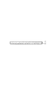
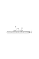
2 絶縁層
3 電気又は電子的な部品
3a 部品本体
3b 端子
6 導体パターン
7 導通ビア
10 接着層
10a 第1の接着体
10b 第2の接着体
11 支持板
12 金属層
13 ビア
14 ボイド
Claims (4)
- 支持板上に形成された金属層に絶縁材料からなる接着層を形成する接着層形成工程と、
前記接着層に電気又は電子的な部品を搭載する部品搭載工程と
を含む部品内蔵基板の製造方法において、
前記部品は部品本体と該部品本体から突出している端子とで形成されていて、
前記接着層は前記金属層と接着される第1の接着体、及び前記部品と接着される第2の接着体からなり、
前記第1の接着体は平面視で前記部品の外縁に略沿って形成され、
前記第2の接着体は平面視で前記端子の外縁と同等あるいは外縁より小さい範囲に塗布形成され、
前記接着層形成工程にて、前記第1の接着体を硬化させた後、前記第2の接着体を前記第1の接着体上に形成することを特徴とする部品内蔵基板の製造方法。 - 前記接着層形成工程にて、前記第2の接着体は平面視で前記端子の外縁より小さく塗布形成されることを特徴とする請求項1に記載の部品内蔵基板の製造方法。
- 前記部品搭載工程の後に行われ、前記部品に対して絶縁層となるべき絶縁材を積層して前記絶縁材内に前記部品を埋設する積層工程と、
前記支持板を除去し、前記金属層及び前記接着層を貫通し前記端子まで到達するビアを形成するビア形成工程と、
前記ビアの表面にめっきを析出させるめっき工程と、
前記金属層を含む導体パターンを形成するパターン形成工程と
をさらに備えたことを特徴とする請求項1に記載の部品内蔵基板の製造方法。 - 部品内蔵基板であって、
支持板上に形成された金属層と、
絶縁材料からなり、前記金属層上に形成される接着層と、
前記接着層に搭載され、部品本体と前記部品本体から突出している端子とで形成される電気又は電子的な部品と、を備え、
前記接着層は、前記金属層と接着される第1の接着体、及び前記部品と接着される第2の接着体とを含み、
前記第1の接着体は、平面視で前記部品の外縁に略沿って形成され、
前記第2の接着体は、硬化した前記第1の接着体上に、平面視で前記端子の外縁と同等あるいは外縁より小さい範囲に形成されていることを特徴とする部品内蔵基板。
Applications Claiming Priority (1)
| Application Number | Priority Date | Filing Date | Title |
|---|---|---|---|
| PCT/JP2012/073205 WO2014041602A1 (ja) | 2012-09-11 | 2012-09-11 | 部品内蔵基板の製造方法及びこれを用いた部品内蔵基板 |
Publications (2)
| Publication Number | Publication Date |
|---|---|
| JPWO2014041602A1 JPWO2014041602A1 (ja) | 2016-08-12 |
| JP6073339B2 true JP6073339B2 (ja) | 2017-02-01 |
Family
ID=50277760
Family Applications (1)
| Application Number | Title | Priority Date | Filing Date |
|---|---|---|---|
| JP2014535252A Active JP6073339B2 (ja) | 2012-09-11 | 2012-09-11 | 部品内蔵基板の製造方法及びこれを用いた部品内蔵基板 |
Country Status (5)
| Country | Link |
|---|---|
| US (1) | US9355990B2 (ja) |
| EP (1) | EP2897446B1 (ja) |
| JP (1) | JP6073339B2 (ja) |
| TW (1) | TW201412218A (ja) |
| WO (1) | WO2014041602A1 (ja) |
Families Citing this family (2)
| Publication number | Priority date | Publication date | Assignee | Title |
|---|---|---|---|---|
| US2552377A (en) * | 1945-02-08 | 1951-05-08 | Bendix Aviat Corp | Altimeter |
| EP3091822A1 (en) * | 2015-05-08 | 2016-11-09 | AT & S Austria Technologie & Systemtechnik Aktiengesellschaft | Method for the production of an electronic module as well as corresponding electronic module |
Family Cites Families (10)
| Publication number | Priority date | Publication date | Assignee | Title |
|---|---|---|---|---|
| JP2002190661A (ja) * | 2000-10-10 | 2002-07-05 | Matsushita Electric Ind Co Ltd | 電子部品の実装体および実装体のリペアー方法 |
| FI20041525A7 (fi) * | 2004-11-26 | 2006-03-17 | Imbera Electronics Oy | Elektroniikkamoduuli ja menetelmä sen valmistamiseksi |
| US8024858B2 (en) * | 2008-02-14 | 2011-09-27 | Ibiden Co., Ltd. | Method of manufacturing printed wiring board with built-in electronic component |
| FI123205B (fi) * | 2008-05-12 | 2012-12-31 | Imbera Electronics Oy | Piirimoduuli ja menetelmä piirimoduulin valmistamiseksi |
| JP4874305B2 (ja) | 2008-07-22 | 2012-02-15 | 株式会社メイコー | 電気・電子部品内蔵回路基板とその製造方法 |
| FI122216B (fi) * | 2009-01-05 | 2011-10-14 | Imbera Electronics Oy | Rigid-flex moduuli |
| US20100212946A1 (en) * | 2009-02-20 | 2010-08-26 | Ibiden Co., Ltd | Wiring board and method for manufacturing the same |
| US8779569B2 (en) * | 2010-01-18 | 2014-07-15 | Rohm Co., Ltd. | Semiconductor device and method for manufacturing the same |
| KR101713640B1 (ko) * | 2010-09-10 | 2017-03-08 | 메이코 일렉트로닉스 컴파니 리미티드 | 부품 내장 기판 |
| KR101562597B1 (ko) * | 2011-07-11 | 2015-10-22 | 가부시키가이샤 무라타 세이사쿠쇼 | 전자부품 |
-
2012
- 2012-09-11 WO PCT/JP2012/073205 patent/WO2014041602A1/ja not_active Ceased
- 2012-09-11 JP JP2014535252A patent/JP6073339B2/ja active Active
- 2012-09-11 US US14/423,990 patent/US9355990B2/en active Active
- 2012-09-11 EP EP12884539.3A patent/EP2897446B1/en not_active Not-in-force
-
2013
- 2013-06-21 TW TW102122096A patent/TW201412218A/zh unknown
Also Published As
| Publication number | Publication date |
|---|---|
| EP2897446A1 (en) | 2015-07-22 |
| TW201412218A (zh) | 2014-03-16 |
| WO2014041602A1 (ja) | 2014-03-20 |
| US9355990B2 (en) | 2016-05-31 |
| JPWO2014041602A1 (ja) | 2016-08-12 |
| EP2897446A4 (en) | 2016-08-03 |
| EP2897446B1 (en) | 2022-03-30 |
| US20150243628A1 (en) | 2015-08-27 |
Similar Documents
| Publication | Publication Date | Title |
|---|---|---|
| TWI519223B (zh) | 多層配線基板之製造方法 | |
| JP5027193B2 (ja) | 配線板及びその製造方法 | |
| JP5581828B2 (ja) | 積層回路基板および基板製造方法 | |
| JP6084283B2 (ja) | 部品内蔵基板及びその製造方法 | |
| KR20150083424A (ko) | 배선 기판의 제조 방법 | |
| JP2013183029A (ja) | 電子部品内蔵配線板及びその製造方法 | |
| JP6073339B2 (ja) | 部品内蔵基板の製造方法及びこれを用いた部品内蔵基板 | |
| JP5695205B2 (ja) | 部品内蔵基板の製造方法及びこれを用いた部品内蔵基板 | |
| TW201316856A (zh) | 內藏元件之基板及其製造方法 | |
| JP5557320B2 (ja) | 配線基板の製造方法 | |
| JP5409480B2 (ja) | 配線基板の製造方法 | |
| WO2012164720A1 (ja) | 部品内蔵基板及びその製造方法 | |
| JP5409519B2 (ja) | 配線基板およびその製造方法 | |
| JP2014192224A (ja) | 配線基板の製造方法 | |
| JP6075789B2 (ja) | 配線基板の製造方法 | |
| JP5360404B2 (ja) | 部品内蔵基板の製造方法 | |
| WO2014041628A1 (ja) | 部品内蔵基板及びその製造方法 | |
| JP2007311466A (ja) | 多層プリント配線基板及びその製造方法 | |
| JP2007311723A (ja) | 多層回路基板 | |
| JP2016092229A (ja) | 多層基板及びその製造方法 | |
| JP2014049531A (ja) | 部品内蔵配線基板の製造方法 | |
| WO2014041697A1 (ja) | 部品内蔵基板及びその製造方法 |
Legal Events
| Date | Code | Title | Description |
|---|---|---|---|
| A131 | Notification of reasons for refusal |
Free format text: JAPANESE INTERMEDIATE CODE: A131 Effective date: 20160817 |
|
| A521 | Request for written amendment filed |
Free format text: JAPANESE INTERMEDIATE CODE: A523 Effective date: 20161005 |
|
| TRDD | Decision of grant or rejection written | ||
| A01 | Written decision to grant a patent or to grant a registration (utility model) |
Free format text: JAPANESE INTERMEDIATE CODE: A01 Effective date: 20161221 |
|
| A61 | First payment of annual fees (during grant procedure) |
Free format text: JAPANESE INTERMEDIATE CODE: A61 Effective date: 20170104 |
|
| R150 | Certificate of patent or registration of utility model |
Ref document number: 6073339 Country of ref document: JP Free format text: JAPANESE INTERMEDIATE CODE: R150 |
|
| R250 | Receipt of annual fees |
Free format text: JAPANESE INTERMEDIATE CODE: R250 |
|
| R250 | Receipt of annual fees |
Free format text: JAPANESE INTERMEDIATE CODE: R250 |
|
| R250 | Receipt of annual fees |
Free format text: JAPANESE INTERMEDIATE CODE: R250 |
|
| R250 | Receipt of annual fees |
Free format text: JAPANESE INTERMEDIATE CODE: R250 |