JP6073530B2 - 電磁波検出器および電磁波検出器アレイ - Google Patents
電磁波検出器および電磁波検出器アレイ Download PDFInfo
- Publication number
- JP6073530B2 JP6073530B2 JP2016532011A JP2016532011A JP6073530B2 JP 6073530 B2 JP6073530 B2 JP 6073530B2 JP 2016532011 A JP2016532011 A JP 2016532011A JP 2016532011 A JP2016532011 A JP 2016532011A JP 6073530 B2 JP6073530 B2 JP 6073530B2
- Authority
- JP
- Japan
- Prior art keywords
- electromagnetic wave
- wave detector
- graphene
- electrode
- layer
- Prior art date
- Legal status (The legal status is an assumption and is not a legal conclusion. Google has not performed a legal analysis and makes no representation as to the accuracy of the status listed.)
- Active
Links
Images




Classifications
-
- H—ELECTRICITY
- H10—SEMICONDUCTOR DEVICES; ELECTRIC SOLID-STATE DEVICES NOT OTHERWISE PROVIDED FOR
- H10F—INORGANIC SEMICONDUCTOR DEVICES SENSITIVE TO INFRARED RADIATION, LIGHT, ELECTROMAGNETIC RADIATION OF SHORTER WAVELENGTH OR CORPUSCULAR RADIATION
- H10F39/00—Integrated devices, or assemblies of multiple devices, comprising at least one element covered by group H10F30/00, e.g. radiation detectors comprising photodiode arrays
- H10F39/10—Integrated devices
- H10F39/107—Integrated devices having multiple elements covered by H10F30/00 in a repetitive configuration, e.g. radiation detectors comprising photodiode arrays
-
- H—ELECTRICITY
- H10—SEMICONDUCTOR DEVICES; ELECTRIC SOLID-STATE DEVICES NOT OTHERWISE PROVIDED FOR
- H10F—INORGANIC SEMICONDUCTOR DEVICES SENSITIVE TO INFRARED RADIATION, LIGHT, ELECTROMAGNETIC RADIATION OF SHORTER WAVELENGTH OR CORPUSCULAR RADIATION
- H10F30/00—Individual radiation-sensitive semiconductor devices in which radiation controls the flow of current through the devices, e.g. photodetectors
- H10F30/20—Individual radiation-sensitive semiconductor devices in which radiation controls the flow of current through the devices, e.g. photodetectors the devices having potential barriers, e.g. phototransistors
- H10F30/21—Individual radiation-sensitive semiconductor devices in which radiation controls the flow of current through the devices, e.g. photodetectors the devices having potential barriers, e.g. phototransistors the devices being sensitive to infrared, visible or ultraviolet radiation
- H10F30/22—Individual radiation-sensitive semiconductor devices in which radiation controls the flow of current through the devices, e.g. photodetectors the devices having potential barriers, e.g. phototransistors the devices being sensitive to infrared, visible or ultraviolet radiation the devices having only one potential barrier, e.g. photodiodes
-
- H—ELECTRICITY
- H10—SEMICONDUCTOR DEVICES; ELECTRIC SOLID-STATE DEVICES NOT OTHERWISE PROVIDED FOR
- H10F—INORGANIC SEMICONDUCTOR DEVICES SENSITIVE TO INFRARED RADIATION, LIGHT, ELECTROMAGNETIC RADIATION OF SHORTER WAVELENGTH OR CORPUSCULAR RADIATION
- H10F39/00—Integrated devices, or assemblies of multiple devices, comprising at least one element covered by group H10F30/00, e.g. radiation detectors comprising photodiode arrays
- H10F39/80—Constructional details of image sensors
-
- H—ELECTRICITY
- H10—SEMICONDUCTOR DEVICES; ELECTRIC SOLID-STATE DEVICES NOT OTHERWISE PROVIDED FOR
- H10F—INORGANIC SEMICONDUCTOR DEVICES SENSITIVE TO INFRARED RADIATION, LIGHT, ELECTROMAGNETIC RADIATION OF SHORTER WAVELENGTH OR CORPUSCULAR RADIATION
- H10F39/00—Integrated devices, or assemblies of multiple devices, comprising at least one element covered by group H10F30/00, e.g. radiation detectors comprising photodiode arrays
- H10F39/80—Constructional details of image sensors
- H10F39/803—Pixels having integrated switching, control, storage or amplification elements
- H10F39/8037—Pixels having integrated switching, control, storage or amplification elements the integrated elements comprising a transistor
-
- H—ELECTRICITY
- H10—SEMICONDUCTOR DEVICES; ELECTRIC SOLID-STATE DEVICES NOT OTHERWISE PROVIDED FOR
- H10F—INORGANIC SEMICONDUCTOR DEVICES SENSITIVE TO INFRARED RADIATION, LIGHT, ELECTROMAGNETIC RADIATION OF SHORTER WAVELENGTH OR CORPUSCULAR RADIATION
- H10F77/00—Constructional details of devices covered by this subclass
- H10F77/10—Semiconductor bodies
- H10F77/12—Active materials
- H10F77/122—Active materials comprising only Group IV materials
Landscapes
- Light Receiving Elements (AREA)
- Photometry And Measurement Of Optical Pulse Characteristics (AREA)
- Solid State Image Pick-Up Elements (AREA)
Description
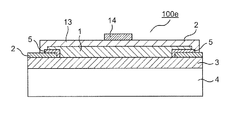
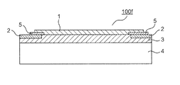
そこで、次世代の検出層の材料としてバンドギャップがゼロまたは極めて小さいグラフェンが注目され、例えば引用文献1では、基板上にゲート酸化膜を設け、その上にグラフェンのチャネル層を堆積し、チャネル層の両端にソースおよびドレインを形成した電磁波検出器が提案されている。
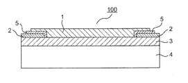
図1は、全体が100で表される、本発明の実施の形態1にかかる電磁波検出器の上面図であり、図2は、図1のI−Iにおける断面図である。
なお、バッファ層5は「層」という表現を用いているが、原子層レベルで見た場合、疎密があるかまたは不連続な領域があっても良い。具体的にはナノ粒子を用いても良い。
図6は、全体が110で表される、本発明の実施の形態2にかかる電磁波検出器の上面図であり、図7は、図6のV−Vにおける断面図である。図6、7中、図1、2と同一符合は、同一または相当箇所を示す。
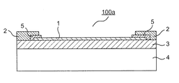
図8は、全体が120で表される、本発明の実施の形態3にかかる電磁波検出器の断面図である。図8中、図1、2と同一符合は、同一または相当箇所を示す。
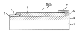
図9は、全体が130で表される、本発明の実施の形態4にかかる電磁波検出器の断面図である。図9中、図1、2と同一符合は、同一または相当箇所を示す。
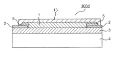
図10は、全体が140で表される、本発明の実施の形態5にかかる電磁波検出器の断面図である。図10中、図1、2と同一符合は、同一または相当箇所を示す。
図13、14は、本実施の形態6にかかる電磁波検出器に用いられるグラフェン層1のみを示した上面図である。実施の形態1にかかる電磁波検出器100と異なる点は、グラフェン層1に、一次元または二次元の周期的な凹部20、21が形成されている点である。凹部20、21は、グラフェン層1を貫通する孔でも良い。グラフェン層1が単層の場合は、凹部20、21は、グラフェン層1を貫通する孔となる。グラフェン層1が複数層の場合は、そのうちのいずれかの層のみを貫通する孔であれば、凹部20、21はグラフェン層1を貫通しない。また、複数層全てを貫通する孔であれば、凹部20、21はグラフェン層1を貫通する。
本実施の形態7にかかる電磁波検出器(図示せず)は、実施の形態1にかかる電磁波検出器100と、グラフェン層1の代わりに遷移金属ダイカルコゲナイドか黒リン(Black Phosphorus)などの2次元材料を用いた点で異なる。他の構造は電磁波検出器100と同様である。遷移金属ダイカルコゲナイドや黒リンなどの2次元材料は、グラフェンと同様の原子層状構造を有するため、2次元材料と呼ばれ、例えばMoS2、WS2、WSe2等遷移金属ダイカルコゲナイドや黒リンからなる。また、これらの材料のうち同種の材料、あるいは異なる材料同士を積層した構造でも良い。あるいはプロベスカイトとグラフェンまたは2次元材料の異種材料接合でもよい。
図15は、全体が1000で表される、本発明の実施の形態8にかかる電磁波検出器アレイの上面図である。図15では、実施の形態1にかかる電磁波検出器100が2×2に配置されているが、配置する個数はこれに限定されるものではない。
図16は、全体が2000で表される、本発明の実施の形態9にかかる電磁波検出器アレイの上面図である。図16では、互いに種類の異なる電磁波検出器100、200、300、400が2×2に配置されているが、配置する個数はこれに限定されるものではない。
2 電極
3 絶縁層
4 基板
5 バッファ層
6、7 電極
8、9 バッファ層
10、11 凹部
12 グラフェン層
13 保護膜
14 電極
100、110、120、130 電磁波検出器
1000、2000 電磁波検出器アレイ
Claims (14)
- 導電性を有する基板と、
該基板の上に設けられた絶縁層と、
該絶縁層の上に設けられたグラフェン層と、
該絶縁層の上に、該グラフェン層を挟んで設けられた一対の電極と、
該グラフェン層と該一対の電極との間にそれぞれ挟まれてこれらを離隔するバッファ層と、を含むことを特徴とする電磁波検出器。 - 上記一対の電極は、同一材料からなることを特徴とする請求項1に記載の電磁波検出器。
- 上記一対の電極の材料が、該電極間で異なることを特徴とする請求項1に記載の電磁波検出器。
- 上記グラフェン層と上記電極との間に、該グラフェン層中のディラックポイントとは異なるディラックポイント(DPe)が形成されることを特徴とする請求項1〜3のいずれかに記載の電磁波検出器。
- 上記電極は金属からなり、上記バッファ層は該金属の酸化物からなることを特徴とする請求項1〜4のいずれかに記載の電磁波検出器。
- 上記グラフェン層および上記バッファ層を覆うように保護膜が設けられたことを特徴とする請求項1〜5のいずれかに記載の電磁波検出器。
- 上記一対の電極において、上記バッファ層を挟んで電極と上記グラフェン層とが対向する部分の面積が、該電極間で異なることを特徴とする請求項1〜6のいずれかに記載の電磁波検出器。
- 上記一対の電極と上記グラフェン層との間にそれぞれ設けられた上記バッファ層の材料が、該バッファ層間で異なることを特徴とする請求項1〜7のいずれかに記載の電磁波検出器。
- 上記電極の表面に、表面プラズモン共鳴を生じる周期的な凹部または凸部が形成されたことを特徴とする請求項1〜8のいずれかに記載の電磁波検出器。
- 上記グラフェンの表面に、表面プラズモン共鳴を生じる周期的な凹部または凸部が形成されたことを特徴とする請求項1〜9のいずれかに記載の電磁波検出器。
- 上記周期的な凹部は、1次元または2次元に配置された周期的な孔、または並列配置された1次元の溝からなることを特徴とする請求項9または10に記載の電磁波検出器。
- 上記グラフェン層は、2層以上のグラフェンの積層構造、または2次元材料、または2次元材料の積層構造、グラフェンと2次元材料との積層構造を有することを特徴とする請求項1〜11のいずれかに記載の電磁波検出器。
- 請求項1〜12のいずれかに記載の電磁波検出器をアレイ状に配置したことを特徴とする電磁波検出器アレイ。
- 請求項9〜12のいずれかに記載の電磁波検出器であって、互いに異なる電磁波検出器をアレイ状に配置したことを特徴とする電磁波検出器アレイ。
Applications Claiming Priority (3)
| Application Number | Priority Date | Filing Date | Title |
|---|---|---|---|
| JP2015014183 | 2015-01-28 | ||
| JP2015014183 | 2015-01-28 | ||
| PCT/JP2016/050026 WO2016121408A1 (ja) | 2015-01-28 | 2016-01-04 | 電磁波検出器および電磁波検出器アレイ |
Publications (2)
| Publication Number | Publication Date |
|---|---|
| JP6073530B2 true JP6073530B2 (ja) | 2017-02-01 |
| JPWO2016121408A1 JPWO2016121408A1 (ja) | 2017-04-27 |
Family
ID=56543030
Family Applications (1)
| Application Number | Title | Priority Date | Filing Date |
|---|---|---|---|
| JP2016532011A Active JP6073530B2 (ja) | 2015-01-28 | 2016-01-04 | 電磁波検出器および電磁波検出器アレイ |
Country Status (5)
| Country | Link |
|---|---|
| US (1) | US10068934B2 (ja) |
| JP (1) | JP6073530B2 (ja) |
| CN (1) | CN107210326B (ja) |
| DE (1) | DE112016000504B4 (ja) |
| WO (1) | WO2016121408A1 (ja) |
Cited By (2)
| Publication number | Priority date | Publication date | Assignee | Title |
|---|---|---|---|---|
| KR101940422B1 (ko) * | 2017-10-02 | 2019-01-21 | 재단법인대구경북과학기술원 | 마이크로파 검출소자 및 마이크로파 검출소자의 제조방법 |
| KR101990050B1 (ko) * | 2017-12-14 | 2019-09-30 | 재단법인 한국탄소융합기술원 | 전이금속 이유화 물질 광소자의 감도 조절 방법 |
Families Citing this family (22)
| Publication number | Priority date | Publication date | Assignee | Title |
|---|---|---|---|---|
| US20170237918A1 (en) * | 2016-02-12 | 2017-08-17 | The Regents Of The University Of Michigan | Light field imaging with transparent photodetectors |
| CN106711260A (zh) * | 2017-02-28 | 2017-05-24 | 刘泉 | 一种石墨烯太阳能板及含有其的路灯 |
| EP3595014B1 (en) * | 2017-03-10 | 2023-05-17 | Mitsubishi Electric Corporation | Electromagnetic wave detector, electromagnetic wave detector array, and electromagnetic wave detection method |
| US11353360B2 (en) * | 2017-03-22 | 2022-06-07 | Mitsubishi Electric Corporation | Electromagnetic wave detector, electromagnetic wave detector array, and electromagnetic wave detection method |
| US10620053B2 (en) * | 2017-05-26 | 2020-04-14 | The Boeing Company | Thermal imaging system |
| JP6918591B2 (ja) * | 2017-06-16 | 2021-08-11 | 株式会社豊田中央研究所 | 電磁波検出器およびその製造方法 |
| US11022486B2 (en) * | 2018-02-12 | 2021-06-01 | National University Of Singapore | MoS2 based photosensor for detecting both light wavelength and intensity |
| EP3783669B1 (en) * | 2018-06-26 | 2023-11-29 | Hangzhou Sanhua Research Institute Co., Ltd. | Infrared sensor and infrared gas detector |
| JP6991330B2 (ja) * | 2018-06-26 | 2022-02-03 | 三菱電機株式会社 | 電磁波検出器および電磁波検出器アレイ |
| JP6642769B1 (ja) * | 2018-06-28 | 2020-02-12 | 三菱電機株式会社 | グラフェンを用いた電子デバイスの製造方法 |
| CN109037372B (zh) * | 2018-07-20 | 2019-12-24 | 大连民族大学 | 一种基于氧化钼微米带/p型Si的多波段光响应器件及其制备方法 |
| US10818865B2 (en) * | 2018-10-17 | 2020-10-27 | Lakeside Photoelectronic Technology (Jiangsu) Co., Ltd. | Multiple hole injection structure on oxidized aluminum and applications thereof in organic luminescent devices |
| JP7260736B2 (ja) | 2018-11-08 | 2023-04-19 | 富士通株式会社 | 光検出素子、光センサ、及び光検出素子の製造方法 |
| US10950638B2 (en) | 2019-03-29 | 2021-03-16 | Toyota Motor Engineering & Manufacturing North America, Inc. | Tunable imaging systems and methods thereof |
| CN110783423A (zh) * | 2019-09-09 | 2020-02-11 | 浙江大学 | 石墨烯/三氧化二铝/砷化镓太赫兹探测器及其制作方法 |
| US20220399466A1 (en) * | 2019-09-30 | 2022-12-15 | Keio University | Graphene photodetector and photodetector array using same |
| CN114222902A (zh) * | 2019-10-10 | 2022-03-22 | 索尼半导体解决方案公司 | 电磁波检测装置、电磁波检测系统和电磁波检测方法 |
| JP7338491B2 (ja) * | 2020-01-27 | 2023-09-05 | 富士通株式会社 | 光センサ装置 |
| JP7563184B2 (ja) * | 2021-01-07 | 2024-10-08 | 富士通株式会社 | 光学センサデバイス、及び光学センサデバイスの製造方法 |
| JP7587132B2 (ja) | 2021-01-08 | 2024-11-20 | 富士通株式会社 | 電子装置、電子装置の製造方法及び電子機器 |
| CN115100830B (zh) * | 2022-07-01 | 2023-05-16 | 中国人民解放军国防科技大学 | 基于等离子体及光敏二极管的高功率微波探测告警平台 |
| CN115453433B (zh) * | 2022-11-09 | 2023-01-20 | 南方电网数字电网研究院有限公司 | 石墨烯非对称结构磁传感器及其参数确定方法 |
Family Cites Families (18)
| Publication number | Priority date | Publication date | Assignee | Title |
|---|---|---|---|---|
| US8053782B2 (en) | 2009-08-24 | 2011-11-08 | International Business Machines Corporation | Single and few-layer graphene based photodetecting devices |
| WO2011058544A2 (en) | 2009-11-16 | 2011-05-19 | Nextpv Inc. | Graphene-based photovoltaic device |
| SG10201503073QA (en) * | 2010-05-05 | 2015-06-29 | Univ Singapore | Hole doping of graphene |
| JP5454394B2 (ja) | 2010-07-09 | 2014-03-26 | ソニー株式会社 | 光電変換素子及び固体撮像装置 |
| JP5150690B2 (ja) * | 2010-09-16 | 2013-02-20 | 株式会社東芝 | 半導体装置及び半導体装置の製造方法 |
| WO2012093360A1 (en) * | 2011-01-04 | 2012-07-12 | Ecole Polytechnique Federale De Lausanne (Epfl) | Semiconductor device |
| US8872159B2 (en) * | 2011-09-29 | 2014-10-28 | The United States Of America, As Represented By The Secretary Of The Navy | Graphene on semiconductor detector |
| KR101539671B1 (ko) * | 2011-11-21 | 2015-07-27 | 삼성전자주식회사 | 복합 투명 전극을 포함하는 그래핀 기반 포토 디텍터와 그 제조방법 및 포토 디텍터를 포함하는 장치 |
| US8983251B2 (en) * | 2011-12-09 | 2015-03-17 | Rochester Institute Of Technology | Electro-optical waveguide apparatuses and methods thereof |
| US8748957B2 (en) * | 2012-01-05 | 2014-06-10 | Quantum Devices, Llc | Coherent spin field effect transistor |
| US9685559B2 (en) * | 2012-12-21 | 2017-06-20 | The Regents Of The University Of California | Vertically stacked heterostructures including graphene |
| KR101423925B1 (ko) * | 2012-12-21 | 2014-07-28 | 광주과학기술원 | 그래핀 다치 로직 소자, 이의 동작방법 및 이의 제조방법 |
| KR102113255B1 (ko) * | 2013-02-22 | 2020-05-20 | 삼성전자주식회사 | 그래핀 적층 구조체의 제조방법, 및 그래핀 적층 구조체와 이를 구비하는 전기소자 |
| US9680038B2 (en) * | 2013-03-13 | 2017-06-13 | The Regents Of The University Of Michigan | Photodetectors based on double layer heterostructures |
| WO2014149004A1 (en) * | 2013-03-22 | 2014-09-25 | Nanyang Technological University | Method of manufacturing a monolayer graphene photodetector and monolayer graphene photodetector |
| JP6128020B2 (ja) | 2013-04-10 | 2017-05-17 | ソニー株式会社 | 電子デバイス及び固体撮像装置、並びに、電子デバイスにおける電極形成方法 |
| JP6161554B2 (ja) * | 2013-04-26 | 2017-07-12 | 三菱電機株式会社 | 電磁波検出器および電磁波検出器アレイ |
| EP3066694B1 (en) * | 2013-11-05 | 2020-10-14 | Nokia Technologies Oy | A photodetection apparatus |
-
2016
- 2016-01-04 CN CN201680007180.3A patent/CN107210326B/zh active Active
- 2016-01-04 JP JP2016532011A patent/JP6073530B2/ja active Active
- 2016-01-04 US US15/540,174 patent/US10068934B2/en active Active
- 2016-01-04 WO PCT/JP2016/050026 patent/WO2016121408A1/ja not_active Ceased
- 2016-01-04 DE DE112016000504.0T patent/DE112016000504B4/de active Active
Cited By (2)
| Publication number | Priority date | Publication date | Assignee | Title |
|---|---|---|---|---|
| KR101940422B1 (ko) * | 2017-10-02 | 2019-01-21 | 재단법인대구경북과학기술원 | 마이크로파 검출소자 및 마이크로파 검출소자의 제조방법 |
| KR101990050B1 (ko) * | 2017-12-14 | 2019-09-30 | 재단법인 한국탄소융합기술원 | 전이금속 이유화 물질 광소자의 감도 조절 방법 |
Also Published As
| Publication number | Publication date |
|---|---|
| DE112016000504B4 (de) | 2024-01-18 |
| CN107210326B (zh) | 2019-02-26 |
| JPWO2016121408A1 (ja) | 2017-04-27 |
| WO2016121408A1 (ja) | 2016-08-04 |
| DE112016000504T5 (de) | 2017-11-16 |
| US20180006067A1 (en) | 2018-01-04 |
| US10068934B2 (en) | 2018-09-04 |
| CN107210326A (zh) | 2017-09-26 |
Similar Documents
| Publication | Publication Date | Title |
|---|---|---|
| JP6073530B2 (ja) | 電磁波検出器および電磁波検出器アレイ | |
| JP6113372B1 (ja) | 電磁波検出器 | |
| JP6297233B1 (ja) | 電磁波検出器及び電磁波検出器アレイ | |
| CN111788700B (zh) | 电磁波检测器以及具备该电磁波检测器的电磁波检测器阵列 | |
| US11353360B2 (en) | Electromagnetic wave detector, electromagnetic wave detector array, and electromagnetic wave detection method | |
| JP6642769B1 (ja) | グラフェンを用いた電子デバイスの製造方法 | |
| JP6528918B1 (ja) | 電磁波検出器及びそれを備えた電磁波検出器アレイ | |
| JP7499857B2 (ja) | 電磁波検出器および電磁波検出器集合体 | |
| JPWO2018163496A1 (ja) | 電磁波検出器、電磁波検出器アレイおよび電磁波検出方法 | |
| US20250327704A1 (en) | Electromagnetic wave detector and electromagnetic wave detector array | |
| JP7345593B2 (ja) | 電磁波検出器および電磁波検出器アレイ | |
| JP7562054B1 (ja) | 電磁波検出器及び電磁波検出器アレイ |
Legal Events
| Date | Code | Title | Description |
|---|---|---|---|
| A521 | Request for written amendment filed |
Free format text: JAPANESE INTERMEDIATE CODE: A523 Effective date: 20160517 |
|
| A621 | Written request for application examination |
Free format text: JAPANESE INTERMEDIATE CODE: A621 Effective date: 20160517 |
|
| A871 | Explanation of circumstances concerning accelerated examination |
Free format text: JAPANESE INTERMEDIATE CODE: A871 Effective date: 20160517 |
|
| A975 | Report on accelerated examination |
Free format text: JAPANESE INTERMEDIATE CODE: A971005 Effective date: 20160707 |
|
| A131 | Notification of reasons for refusal |
Free format text: JAPANESE INTERMEDIATE CODE: A131 Effective date: 20160802 |
|
| A521 | Request for written amendment filed |
Free format text: JAPANESE INTERMEDIATE CODE: A523 Effective date: 20160929 |
|
| TRDD | Decision of grant or rejection written | ||
| A01 | Written decision to grant a patent or to grant a registration (utility model) |
Free format text: JAPANESE INTERMEDIATE CODE: A01 Effective date: 20161206 |
|
| A61 | First payment of annual fees (during grant procedure) |
Free format text: JAPANESE INTERMEDIATE CODE: A61 Effective date: 20170104 |
|
| R150 | Certificate of patent or registration of utility model |
Ref document number: 6073530 Country of ref document: JP Free format text: JAPANESE INTERMEDIATE CODE: R150 |
|
| R250 | Receipt of annual fees |
Free format text: JAPANESE INTERMEDIATE CODE: R250 |
|
| R250 | Receipt of annual fees |
Free format text: JAPANESE INTERMEDIATE CODE: R250 |
|
| R250 | Receipt of annual fees |
Free format text: JAPANESE INTERMEDIATE CODE: R250 |
|
| R250 | Receipt of annual fees |
Free format text: JAPANESE INTERMEDIATE CODE: R250 |
|
| R250 | Receipt of annual fees |
Free format text: JAPANESE INTERMEDIATE CODE: R250 |
|
| R250 | Receipt of annual fees |
Free format text: JAPANESE INTERMEDIATE CODE: R250 |
|
| R250 | Receipt of annual fees |
Free format text: JAPANESE INTERMEDIATE CODE: R250 |