JP6098064B2 - 表示装置および照明装置 - Google Patents
表示装置および照明装置 Download PDFInfo
- Publication number
- JP6098064B2 JP6098064B2 JP2012176490A JP2012176490A JP6098064B2 JP 6098064 B2 JP6098064 B2 JP 6098064B2 JP 2012176490 A JP2012176490 A JP 2012176490A JP 2012176490 A JP2012176490 A JP 2012176490A JP 6098064 B2 JP6098064 B2 JP 6098064B2
- Authority
- JP
- Japan
- Prior art keywords
- light
- electrode
- scattering
- linear
- illumination
- Prior art date
- Legal status (The legal status is an assumption and is not a legal conclusion. Google has not performed a legal analysis and makes no representation as to the accuracy of the status listed.)
- Expired - Fee Related
Links
Images


































Classifications
-
- G—PHYSICS
- G02—OPTICS
- G02F—OPTICAL DEVICES OR ARRANGEMENTS FOR THE CONTROL OF LIGHT BY MODIFICATION OF THE OPTICAL PROPERTIES OF THE MEDIA OF THE ELEMENTS INVOLVED THEREIN; NON-LINEAR OPTICS; FREQUENCY-CHANGING OF LIGHT; OPTICAL LOGIC ELEMENTS; OPTICAL ANALOGUE/DIGITAL CONVERTERS
- G02F1/00—Devices or arrangements for the control of the intensity, colour, phase, polarisation or direction of light arriving from an independent light source, e.g. switching, gating or modulating; Non-linear optics
- G02F1/01—Devices or arrangements for the control of the intensity, colour, phase, polarisation or direction of light arriving from an independent light source, e.g. switching, gating or modulating; Non-linear optics for the control of the intensity, phase, polarisation or colour
- G02F1/13—Devices or arrangements for the control of the intensity, colour, phase, polarisation or direction of light arriving from an independent light source, e.g. switching, gating or modulating; Non-linear optics for the control of the intensity, phase, polarisation or colour based on liquid crystals, e.g. single liquid crystal display cells
- G02F1/133—Constructional arrangements; Operation of liquid crystal cells; Circuit arrangements
- G02F1/1333—Constructional arrangements; Manufacturing methods
- G02F1/1335—Structural association of cells with optical devices, e.g. polarisers or reflectors
- G02F1/133526—Lenses, e.g. microlenses or Fresnel lenses
-
- G—PHYSICS
- G02—OPTICS
- G02B—OPTICAL ELEMENTS, SYSTEMS OR APPARATUS
- G02B3/00—Simple or compound lenses
- G02B3/0006—Arrays
- G02B3/0037—Arrays characterized by the distribution or form of lenses
- G02B3/0043—Inhomogeneous or irregular arrays, e.g. varying shape, size, height
-
- G—PHYSICS
- G02—OPTICS
- G02B—OPTICAL ELEMENTS, SYSTEMS OR APPARATUS
- G02B3/00—Simple or compound lenses
- G02B3/0006—Arrays
- G02B3/0037—Arrays characterized by the distribution or form of lenses
- G02B3/005—Arrays characterized by the distribution or form of lenses arranged along a single direction only, e.g. lenticular sheets
-
- G—PHYSICS
- G02—OPTICS
- G02B—OPTICAL ELEMENTS, SYSTEMS OR APPARATUS
- G02B30/00—Optical systems or apparatus for producing three-dimensional [3D] effects, e.g. stereoscopic images
- G02B30/20—Optical systems or apparatus for producing three-dimensional [3D] effects, e.g. stereoscopic images by providing first and second parallax images to an observer's left and right eyes
- G02B30/26—Optical systems or apparatus for producing three-dimensional [3D] effects, e.g. stereoscopic images by providing first and second parallax images to an observer's left and right eyes of the autostereoscopic type
- G02B30/27—Optical systems or apparatus for producing three-dimensional [3D] effects, e.g. stereoscopic images by providing first and second parallax images to an observer's left and right eyes of the autostereoscopic type involving lenticular arrays
-
- G—PHYSICS
- G02—OPTICS
- G02B—OPTICAL ELEMENTS, SYSTEMS OR APPARATUS
- G02B30/00—Optical systems or apparatus for producing three-dimensional [3D] effects, e.g. stereoscopic images
- G02B30/20—Optical systems or apparatus for producing three-dimensional [3D] effects, e.g. stereoscopic images by providing first and second parallax images to an observer's left and right eyes
- G02B30/26—Optical systems or apparatus for producing three-dimensional [3D] effects, e.g. stereoscopic images by providing first and second parallax images to an observer's left and right eyes of the autostereoscopic type
- G02B30/30—Optical systems or apparatus for producing three-dimensional [3D] effects, e.g. stereoscopic images by providing first and second parallax images to an observer's left and right eyes of the autostereoscopic type involving parallax barriers
-
- G—PHYSICS
- G02—OPTICS
- G02F—OPTICAL DEVICES OR ARRANGEMENTS FOR THE CONTROL OF LIGHT BY MODIFICATION OF THE OPTICAL PROPERTIES OF THE MEDIA OF THE ELEMENTS INVOLVED THEREIN; NON-LINEAR OPTICS; FREQUENCY-CHANGING OF LIGHT; OPTICAL LOGIC ELEMENTS; OPTICAL ANALOGUE/DIGITAL CONVERTERS
- G02F1/00—Devices or arrangements for the control of the intensity, colour, phase, polarisation or direction of light arriving from an independent light source, e.g. switching, gating or modulating; Non-linear optics
- G02F1/01—Devices or arrangements for the control of the intensity, colour, phase, polarisation or direction of light arriving from an independent light source, e.g. switching, gating or modulating; Non-linear optics for the control of the intensity, phase, polarisation or colour
- G02F1/13—Devices or arrangements for the control of the intensity, colour, phase, polarisation or direction of light arriving from an independent light source, e.g. switching, gating or modulating; Non-linear optics for the control of the intensity, phase, polarisation or colour based on liquid crystals, e.g. single liquid crystal display cells
- G02F1/133—Constructional arrangements; Operation of liquid crystal cells; Circuit arrangements
- G02F1/1333—Constructional arrangements; Manufacturing methods
- G02F1/1335—Structural association of cells with optical devices, e.g. polarisers or reflectors
- G02F1/133504—Diffusing, scattering, diffracting elements
-
- G—PHYSICS
- G02—OPTICS
- G02F—OPTICAL DEVICES OR ARRANGEMENTS FOR THE CONTROL OF LIGHT BY MODIFICATION OF THE OPTICAL PROPERTIES OF THE MEDIA OF THE ELEMENTS INVOLVED THEREIN; NON-LINEAR OPTICS; FREQUENCY-CHANGING OF LIGHT; OPTICAL LOGIC ELEMENTS; OPTICAL ANALOGUE/DIGITAL CONVERTERS
- G02F1/00—Devices or arrangements for the control of the intensity, colour, phase, polarisation or direction of light arriving from an independent light source, e.g. switching, gating or modulating; Non-linear optics
- G02F1/01—Devices or arrangements for the control of the intensity, colour, phase, polarisation or direction of light arriving from an independent light source, e.g. switching, gating or modulating; Non-linear optics for the control of the intensity, phase, polarisation or colour
- G02F1/13—Devices or arrangements for the control of the intensity, colour, phase, polarisation or direction of light arriving from an independent light source, e.g. switching, gating or modulating; Non-linear optics for the control of the intensity, phase, polarisation or colour based on liquid crystals, e.g. single liquid crystal display cells
- G02F1/133—Constructional arrangements; Operation of liquid crystal cells; Circuit arrangements
- G02F1/1333—Constructional arrangements; Manufacturing methods
- G02F1/1335—Structural association of cells with optical devices, e.g. polarisers or reflectors
- G02F1/133528—Polarisers
-
- G—PHYSICS
- G02—OPTICS
- G02F—OPTICAL DEVICES OR ARRANGEMENTS FOR THE CONTROL OF LIGHT BY MODIFICATION OF THE OPTICAL PROPERTIES OF THE MEDIA OF THE ELEMENTS INVOLVED THEREIN; NON-LINEAR OPTICS; FREQUENCY-CHANGING OF LIGHT; OPTICAL LOGIC ELEMENTS; OPTICAL ANALOGUE/DIGITAL CONVERTERS
- G02F1/00—Devices or arrangements for the control of the intensity, colour, phase, polarisation or direction of light arriving from an independent light source, e.g. switching, gating or modulating; Non-linear optics
- G02F1/01—Devices or arrangements for the control of the intensity, colour, phase, polarisation or direction of light arriving from an independent light source, e.g. switching, gating or modulating; Non-linear optics for the control of the intensity, phase, polarisation or colour
- G02F1/13—Devices or arrangements for the control of the intensity, colour, phase, polarisation or direction of light arriving from an independent light source, e.g. switching, gating or modulating; Non-linear optics for the control of the intensity, phase, polarisation or colour based on liquid crystals, e.g. single liquid crystal display cells
- G02F1/133—Constructional arrangements; Operation of liquid crystal cells; Circuit arrangements
- G02F1/1333—Constructional arrangements; Manufacturing methods
- G02F1/1347—Arrangement of liquid crystal layers or cells in which the final condition of one light beam is achieved by the addition of the effects of two or more layers or cells
- G02F1/13476—Arrangement of liquid crystal layers or cells in which the final condition of one light beam is achieved by the addition of the effects of two or more layers or cells in which at least one liquid crystal cell or layer assumes a scattering state
-
- G—PHYSICS
- G09—EDUCATION; CRYPTOGRAPHY; DISPLAY; ADVERTISING; SEALS
- G09G—ARRANGEMENTS OR CIRCUITS FOR CONTROL OF INDICATING DEVICES USING STATIC MEANS TO PRESENT VARIABLE INFORMATION
- G09G3/00—Control arrangements or circuits, of interest only in connection with visual indicators other than cathode-ray tubes
- G09G3/001—Control arrangements or circuits, of interest only in connection with visual indicators other than cathode-ray tubes using specific devices not provided for in groups G09G3/02 - G09G3/36, e.g. using an intermediate record carrier such as a film slide; Projection systems; Display of non-alphanumerical information, solely or in combination with alphanumerical information, e.g. digital display on projected diapositive as background
- G09G3/003—Control arrangements or circuits, of interest only in connection with visual indicators other than cathode-ray tubes using specific devices not provided for in groups G09G3/02 - G09G3/36, e.g. using an intermediate record carrier such as a film slide; Projection systems; Display of non-alphanumerical information, solely or in combination with alphanumerical information, e.g. digital display on projected diapositive as background to produce spatial visual effects
-
- G—PHYSICS
- G09—EDUCATION; CRYPTOGRAPHY; DISPLAY; ADVERTISING; SEALS
- G09G—ARRANGEMENTS OR CIRCUITS FOR CONTROL OF INDICATING DEVICES USING STATIC MEANS TO PRESENT VARIABLE INFORMATION
- G09G3/00—Control arrangements or circuits, of interest only in connection with visual indicators other than cathode-ray tubes
- G09G3/20—Control arrangements or circuits, of interest only in connection with visual indicators other than cathode-ray tubes for presentation of an assembly of a number of characters, e.g. a page, by composing the assembly by combination of individual elements arranged in a matrix no fixed position being assigned to or needed to be assigned to the individual characters or partial characters
- G09G3/34—Control arrangements or circuits, of interest only in connection with visual indicators other than cathode-ray tubes for presentation of an assembly of a number of characters, e.g. a page, by composing the assembly by combination of individual elements arranged in a matrix no fixed position being assigned to or needed to be assigned to the individual characters or partial characters by control of light from an independent source
- G09G3/3406—Control of illumination source
-
- G—PHYSICS
- G09—EDUCATION; CRYPTOGRAPHY; DISPLAY; ADVERTISING; SEALS
- G09G—ARRANGEMENTS OR CIRCUITS FOR CONTROL OF INDICATING DEVICES USING STATIC MEANS TO PRESENT VARIABLE INFORMATION
- G09G3/00—Control arrangements or circuits, of interest only in connection with visual indicators other than cathode-ray tubes
- G09G3/20—Control arrangements or circuits, of interest only in connection with visual indicators other than cathode-ray tubes for presentation of an assembly of a number of characters, e.g. a page, by composing the assembly by combination of individual elements arranged in a matrix no fixed position being assigned to or needed to be assigned to the individual characters or partial characters
- G09G3/34—Control arrangements or circuits, of interest only in connection with visual indicators other than cathode-ray tubes for presentation of an assembly of a number of characters, e.g. a page, by composing the assembly by combination of individual elements arranged in a matrix no fixed position being assigned to or needed to be assigned to the individual characters or partial characters by control of light from an independent source
- G09G3/36—Control arrangements or circuits, of interest only in connection with visual indicators other than cathode-ray tubes for presentation of an assembly of a number of characters, e.g. a page, by composing the assembly by combination of individual elements arranged in a matrix no fixed position being assigned to or needed to be assigned to the individual characters or partial characters by control of light from an independent source using liquid crystals
-
- H—ELECTRICITY
- H04—ELECTRIC COMMUNICATION TECHNIQUE
- H04N—PICTORIAL COMMUNICATION, e.g. TELEVISION
- H04N13/00—Stereoscopic video systems; Multi-view video systems; Details thereof
- H04N13/30—Image reproducers
- H04N13/302—Image reproducers for viewing without the aid of special glasses, i.e. using autostereoscopic displays
- H04N13/305—Image reproducers for viewing without the aid of special glasses, i.e. using autostereoscopic displays using lenticular lenses, e.g. arrangements of cylindrical lenses
-
- H—ELECTRICITY
- H04—ELECTRIC COMMUNICATION TECHNIQUE
- H04N—PICTORIAL COMMUNICATION, e.g. TELEVISION
- H04N13/00—Stereoscopic video systems; Multi-view video systems; Details thereof
- H04N13/30—Image reproducers
- H04N13/302—Image reproducers for viewing without the aid of special glasses, i.e. using autostereoscopic displays
- H04N13/307—Image reproducers for viewing without the aid of special glasses, i.e. using autostereoscopic displays using fly-eye lenses, e.g. arrangements of circular lenses
-
- H—ELECTRICITY
- H04—ELECTRIC COMMUNICATION TECHNIQUE
- H04N—PICTORIAL COMMUNICATION, e.g. TELEVISION
- H04N13/00—Stereoscopic video systems; Multi-view video systems; Details thereof
- H04N13/30—Image reproducers
- H04N13/302—Image reproducers for viewing without the aid of special glasses, i.e. using autostereoscopic displays
- H04N13/31—Image reproducers for viewing without the aid of special glasses, i.e. using autostereoscopic displays using parallax barriers
-
- H—ELECTRICITY
- H04—ELECTRIC COMMUNICATION TECHNIQUE
- H04N—PICTORIAL COMMUNICATION, e.g. TELEVISION
- H04N13/00—Stereoscopic video systems; Multi-view video systems; Details thereof
- H04N13/30—Image reproducers
- H04N13/302—Image reproducers for viewing without the aid of special glasses, i.e. using autostereoscopic displays
- H04N13/31—Image reproducers for viewing without the aid of special glasses, i.e. using autostereoscopic displays using parallax barriers
- H04N13/312—Image reproducers for viewing without the aid of special glasses, i.e. using autostereoscopic displays using parallax barriers the parallax barriers being placed behind the display panel, e.g. between backlight and spatial light modulator [SLM]
-
- H—ELECTRICITY
- H04—ELECTRIC COMMUNICATION TECHNIQUE
- H04N—PICTORIAL COMMUNICATION, e.g. TELEVISION
- H04N13/00—Stereoscopic video systems; Multi-view video systems; Details thereof
- H04N13/30—Image reproducers
- H04N13/302—Image reproducers for viewing without the aid of special glasses, i.e. using autostereoscopic displays
- H04N13/317—Image reproducers for viewing without the aid of special glasses, i.e. using autostereoscopic displays using slanted parallax optics
-
- H—ELECTRICITY
- H04—ELECTRIC COMMUNICATION TECHNIQUE
- H04N—PICTORIAL COMMUNICATION, e.g. TELEVISION
- H04N13/00—Stereoscopic video systems; Multi-view video systems; Details thereof
- H04N13/30—Image reproducers
- H04N13/356—Image reproducers having separate monoscopic and stereoscopic modes
- H04N13/359—Switching between monoscopic and stereoscopic modes
-
- G—PHYSICS
- G02—OPTICS
- G02B—OPTICAL ELEMENTS, SYSTEMS OR APPARATUS
- G02B6/00—Light guides; Structural details of arrangements comprising light guides and other optical elements, e.g. couplings
- G02B6/0001—Light guides; Structural details of arrangements comprising light guides and other optical elements, e.g. couplings specially adapted for lighting devices or systems
- G02B6/0011—Light guides; Structural details of arrangements comprising light guides and other optical elements, e.g. couplings specially adapted for lighting devices or systems the light guides being planar or of plate-like form
- G02B6/0033—Means for improving the coupling-out of light from the light guide
- G02B6/0035—Means for improving the coupling-out of light from the light guide provided on the surface of the light guide or in the bulk of it
- G02B6/0038—Linear indentations or grooves, e.g. arc-shaped grooves or meandering grooves, extending over the full length or width of the light guide
-
- G—PHYSICS
- G02—OPTICS
- G02B—OPTICAL ELEMENTS, SYSTEMS OR APPARATUS
- G02B6/00—Light guides; Structural details of arrangements comprising light guides and other optical elements, e.g. couplings
- G02B6/0001—Light guides; Structural details of arrangements comprising light guides and other optical elements, e.g. couplings specially adapted for lighting devices or systems
- G02B6/0011—Light guides; Structural details of arrangements comprising light guides and other optical elements, e.g. couplings specially adapted for lighting devices or systems the light guides being planar or of plate-like form
- G02B6/0033—Means for improving the coupling-out of light from the light guide
- G02B6/0035—Means for improving the coupling-out of light from the light guide provided on the surface of the light guide or in the bulk of it
- G02B6/0045—Means for improving the coupling-out of light from the light guide provided on the surface of the light guide or in the bulk of it by shaping at least a portion of the light guide
- G02B6/0046—Tapered light guide, e.g. wedge-shaped light guide
-
- G—PHYSICS
- G02—OPTICS
- G02B—OPTICAL ELEMENTS, SYSTEMS OR APPARATUS
- G02B6/00—Light guides; Structural details of arrangements comprising light guides and other optical elements, e.g. couplings
- G02B6/0001—Light guides; Structural details of arrangements comprising light guides and other optical elements, e.g. couplings specially adapted for lighting devices or systems
- G02B6/0011—Light guides; Structural details of arrangements comprising light guides and other optical elements, e.g. couplings specially adapted for lighting devices or systems the light guides being planar or of plate-like form
- G02B6/0033—Means for improving the coupling-out of light from the light guide
- G02B6/0058—Means for improving the coupling-out of light from the light guide varying in density, size, shape or depth along the light guide
- G02B6/0061—Means for improving the coupling-out of light from the light guide varying in density, size, shape or depth along the light guide to provide homogeneous light output intensity
-
- G—PHYSICS
- G02—OPTICS
- G02B—OPTICAL ELEMENTS, SYSTEMS OR APPARATUS
- G02B6/00—Light guides; Structural details of arrangements comprising light guides and other optical elements, e.g. couplings
- G02B6/0001—Light guides; Structural details of arrangements comprising light guides and other optical elements, e.g. couplings specially adapted for lighting devices or systems
- G02B6/0011—Light guides; Structural details of arrangements comprising light guides and other optical elements, e.g. couplings specially adapted for lighting devices or systems the light guides being planar or of plate-like form
- G02B6/0066—Light guides; Structural details of arrangements comprising light guides and other optical elements, e.g. couplings specially adapted for lighting devices or systems the light guides being planar or of plate-like form characterised by the light source being coupled to the light guide
- G02B6/0068—Arrangements of plural sources, e.g. multi-colour light sources
-
- G—PHYSICS
- G02—OPTICS
- G02B—OPTICAL ELEMENTS, SYSTEMS OR APPARATUS
- G02B6/00—Light guides; Structural details of arrangements comprising light guides and other optical elements, e.g. couplings
- G02B6/0001—Light guides; Structural details of arrangements comprising light guides and other optical elements, e.g. couplings specially adapted for lighting devices or systems
- G02B6/0011—Light guides; Structural details of arrangements comprising light guides and other optical elements, e.g. couplings specially adapted for lighting devices or systems the light guides being planar or of plate-like form
- G02B6/0066—Light guides; Structural details of arrangements comprising light guides and other optical elements, e.g. couplings specially adapted for lighting devices or systems the light guides being planar or of plate-like form characterised by the light source being coupled to the light guide
- G02B6/007—Incandescent lamp or gas discharge lamp
- G02B6/0071—Incandescent lamp or gas discharge lamp with elongated shape, e.g. tube
-
- G—PHYSICS
- G02—OPTICS
- G02F—OPTICAL DEVICES OR ARRANGEMENTS FOR THE CONTROL OF LIGHT BY MODIFICATION OF THE OPTICAL PROPERTIES OF THE MEDIA OF THE ELEMENTS INVOLVED THEREIN; NON-LINEAR OPTICS; FREQUENCY-CHANGING OF LIGHT; OPTICAL LOGIC ELEMENTS; OPTICAL ANALOGUE/DIGITAL CONVERTERS
- G02F1/00—Devices or arrangements for the control of the intensity, colour, phase, polarisation or direction of light arriving from an independent light source, e.g. switching, gating or modulating; Non-linear optics
- G02F1/01—Devices or arrangements for the control of the intensity, colour, phase, polarisation or direction of light arriving from an independent light source, e.g. switching, gating or modulating; Non-linear optics for the control of the intensity, phase, polarisation or colour
- G02F1/13—Devices or arrangements for the control of the intensity, colour, phase, polarisation or direction of light arriving from an independent light source, e.g. switching, gating or modulating; Non-linear optics for the control of the intensity, phase, polarisation or colour based on liquid crystals, e.g. single liquid crystal display cells
- G02F1/133—Constructional arrangements; Operation of liquid crystal cells; Circuit arrangements
- G02F1/1333—Constructional arrangements; Manufacturing methods
- G02F1/1334—Constructional arrangements; Manufacturing methods based on polymer dispersed liquid crystals, e.g. microencapsulated liquid crystals
-
- G—PHYSICS
- G02—OPTICS
- G02F—OPTICAL DEVICES OR ARRANGEMENTS FOR THE CONTROL OF LIGHT BY MODIFICATION OF THE OPTICAL PROPERTIES OF THE MEDIA OF THE ELEMENTS INVOLVED THEREIN; NON-LINEAR OPTICS; FREQUENCY-CHANGING OF LIGHT; OPTICAL LOGIC ELEMENTS; OPTICAL ANALOGUE/DIGITAL CONVERTERS
- G02F1/00—Devices or arrangements for the control of the intensity, colour, phase, polarisation or direction of light arriving from an independent light source, e.g. switching, gating or modulating; Non-linear optics
- G02F1/01—Devices or arrangements for the control of the intensity, colour, phase, polarisation or direction of light arriving from an independent light source, e.g. switching, gating or modulating; Non-linear optics for the control of the intensity, phase, polarisation or colour
- G02F1/13—Devices or arrangements for the control of the intensity, colour, phase, polarisation or direction of light arriving from an independent light source, e.g. switching, gating or modulating; Non-linear optics for the control of the intensity, phase, polarisation or colour based on liquid crystals, e.g. single liquid crystal display cells
- G02F1/133—Constructional arrangements; Operation of liquid crystal cells; Circuit arrangements
- G02F1/1333—Constructional arrangements; Manufacturing methods
- G02F1/1335—Structural association of cells with optical devices, e.g. polarisers or reflectors
- G02F1/1336—Illuminating devices
-
- G—PHYSICS
- G02—OPTICS
- G02F—OPTICAL DEVICES OR ARRANGEMENTS FOR THE CONTROL OF LIGHT BY MODIFICATION OF THE OPTICAL PROPERTIES OF THE MEDIA OF THE ELEMENTS INVOLVED THEREIN; NON-LINEAR OPTICS; FREQUENCY-CHANGING OF LIGHT; OPTICAL LOGIC ELEMENTS; OPTICAL ANALOGUE/DIGITAL CONVERTERS
- G02F1/00—Devices or arrangements for the control of the intensity, colour, phase, polarisation or direction of light arriving from an independent light source, e.g. switching, gating or modulating; Non-linear optics
- G02F1/01—Devices or arrangements for the control of the intensity, colour, phase, polarisation or direction of light arriving from an independent light source, e.g. switching, gating or modulating; Non-linear optics for the control of the intensity, phase, polarisation or colour
- G02F1/13—Devices or arrangements for the control of the intensity, colour, phase, polarisation or direction of light arriving from an independent light source, e.g. switching, gating or modulating; Non-linear optics for the control of the intensity, phase, polarisation or colour based on liquid crystals, e.g. single liquid crystal display cells
- G02F1/133—Constructional arrangements; Operation of liquid crystal cells; Circuit arrangements
- G02F1/1333—Constructional arrangements; Manufacturing methods
- G02F1/1335—Structural association of cells with optical devices, e.g. polarisers or reflectors
- G02F1/1336—Illuminating devices
- G02F1/133602—Direct backlight
- G02F1/133606—Direct backlight including a specially adapted diffusing, scattering or light controlling members
-
- G—PHYSICS
- G02—OPTICS
- G02F—OPTICAL DEVICES OR ARRANGEMENTS FOR THE CONTROL OF LIGHT BY MODIFICATION OF THE OPTICAL PROPERTIES OF THE MEDIA OF THE ELEMENTS INVOLVED THEREIN; NON-LINEAR OPTICS; FREQUENCY-CHANGING OF LIGHT; OPTICAL LOGIC ELEMENTS; OPTICAL ANALOGUE/DIGITAL CONVERTERS
- G02F1/00—Devices or arrangements for the control of the intensity, colour, phase, polarisation or direction of light arriving from an independent light source, e.g. switching, gating or modulating; Non-linear optics
- G02F1/01—Devices or arrangements for the control of the intensity, colour, phase, polarisation or direction of light arriving from an independent light source, e.g. switching, gating or modulating; Non-linear optics for the control of the intensity, phase, polarisation or colour
- G02F1/13—Devices or arrangements for the control of the intensity, colour, phase, polarisation or direction of light arriving from an independent light source, e.g. switching, gating or modulating; Non-linear optics for the control of the intensity, phase, polarisation or colour based on liquid crystals, e.g. single liquid crystal display cells
- G02F1/133—Constructional arrangements; Operation of liquid crystal cells; Circuit arrangements
- G02F1/1333—Constructional arrangements; Manufacturing methods
- G02F1/1335—Structural association of cells with optical devices, e.g. polarisers or reflectors
- G02F1/1336—Illuminating devices
- G02F1/133602—Direct backlight
- G02F1/133606—Direct backlight including a specially adapted diffusing, scattering or light controlling members
- G02F1/133607—Direct backlight including a specially adapted diffusing, scattering or light controlling members the light controlling member including light directing or refracting elements, e.g. prisms or lenses
-
- G—PHYSICS
- G02—OPTICS
- G02F—OPTICAL DEVICES OR ARRANGEMENTS FOR THE CONTROL OF LIGHT BY MODIFICATION OF THE OPTICAL PROPERTIES OF THE MEDIA OF THE ELEMENTS INVOLVED THEREIN; NON-LINEAR OPTICS; FREQUENCY-CHANGING OF LIGHT; OPTICAL LOGIC ELEMENTS; OPTICAL ANALOGUE/DIGITAL CONVERTERS
- G02F1/00—Devices or arrangements for the control of the intensity, colour, phase, polarisation or direction of light arriving from an independent light source, e.g. switching, gating or modulating; Non-linear optics
- G02F1/01—Devices or arrangements for the control of the intensity, colour, phase, polarisation or direction of light arriving from an independent light source, e.g. switching, gating or modulating; Non-linear optics for the control of the intensity, phase, polarisation or colour
- G02F1/13—Devices or arrangements for the control of the intensity, colour, phase, polarisation or direction of light arriving from an independent light source, e.g. switching, gating or modulating; Non-linear optics for the control of the intensity, phase, polarisation or colour based on liquid crystals, e.g. single liquid crystal display cells
- G02F1/133—Constructional arrangements; Operation of liquid crystal cells; Circuit arrangements
- G02F1/1333—Constructional arrangements; Manufacturing methods
- G02F1/1335—Structural association of cells with optical devices, e.g. polarisers or reflectors
- G02F1/1336—Illuminating devices
- G02F1/133626—Illuminating devices providing two modes of illumination, e.g. day-night
-
- H—ELECTRICITY
- H04—ELECTRIC COMMUNICATION TECHNIQUE
- H04N—PICTORIAL COMMUNICATION, e.g. TELEVISION
- H04N13/00—Stereoscopic video systems; Multi-view video systems; Details thereof
- H04N13/30—Image reproducers
- H04N13/324—Colour aspects
Landscapes
- Physics & Mathematics (AREA)
- Engineering & Computer Science (AREA)
- Multimedia (AREA)
- Signal Processing (AREA)
- General Physics & Mathematics (AREA)
- Optics & Photonics (AREA)
- Nonlinear Science (AREA)
- Chemical & Material Sciences (AREA)
- Crystallography & Structural Chemistry (AREA)
- Mathematical Physics (AREA)
- Computer Hardware Design (AREA)
- Theoretical Computer Science (AREA)
- Liquid Crystal (AREA)
- Planar Illumination Modules (AREA)
Description
1.第1の実施の形態(照明装置)
2.第1の実施の形態の変形例(照明装置)
3.第2の実施の形態(受信側装置)
4.第2の実施の形態の変形例(受信側装置)
5.実施例
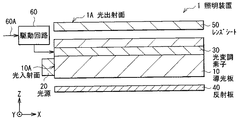
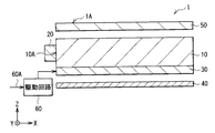
図1は、本技術の第1の実施の形態に係る照明装置1の断面構成を表すものである。この照明装置1は、表示装置のバックライトとして適用可能なものであり、照明光を出力可能なものである。照明装置1は、例えば、導光板10と、導光板10の側面に配置した光源20と、導光板10の内部に配置した光変調素子30と、導光板10の背後に配置した反射板40と、導光板10の上に配置したレンズシート50と、光変調素子30を駆動する駆動回路60とを備えている。
導光板10は、導光板10の側面に配置した光源20からの光を導光板10の上面側(具体的には照明装置1の光出射面1A)に導くものである。導光板10は、例えば、導光板10の上面に配置される被照射物(例えば後述の表示パネル210)に対応した形状になっており、例えば、上面、下面および側面で囲まれた直方体状となっている。なお、以下では、導光板10の側面のうち光源20からの光が入射する側面を光入射面10Aと称するものとする。
光源20は、線状光源であり、例えば、熱陰極管(HCFL;Hot Cathode Fluorescent Lamp)、冷陰極管(CCFL;Cold Cathode Fluorescent Lamp)、または複数のLED(Light Emitting Diode)を一列に配置したものなどからなる。光源20が複数のLEDからなる場合には、効率、薄型化、均一性の観点から、全てのLEDがホワイトLEDであることが好ましい。なお、光源20が、例えば、赤色LED、緑色LEDおよび青色LEDを含んで構成されていてもよい。光源20は、導光板10の一の側面にだけ設けられていてもよいし(図1参照)、導光板10の2つの側面、3つの側面または全ての側面に設けられていてもよい。
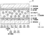
光変調素子30は、本実施の形態において、導光板10の内部に空気層を介さずに密着しており、例えば接着剤(図示せず)を介して導光板10に接着されている。光変調素子30は、例えば、図2に示したように、透明基板31、下側電極32、配向膜33、光変調層34、配向膜35、上側電極36および透明基板37を反射板40側から順に配置したものである。なお、図2は、光変調素子30の断面構成例を表すものである。下側電極32および上側電極36が本技術の「電極」の一具体例に相当する。光変調層34が本技術の「光変調層」の一具体例に相当する。
反射板40は、導光板10の背後から光変調素子30を介して漏れ出てきた光を導光板10側に戻すものである。反射板40は、例えば、反射、拡散、散乱などの機能を有している。これにより、光源20からの出射光を効率的に利用することができ、また、正面輝度の向上にも役立っている。反射板40は、例えば、発泡PET(ポリエチレンテレフタレート)や銀蒸着フィルム、多層膜反射フィルム、白色PETなどからなる。反射板40に正反射(鏡面反射)の機能を持たせる場合には、反射板40は、例えば、銀蒸着フィルム、多層膜反射フィルム、アルミニウム蒸着フィルムなどで構成されていることが好ましい。また、反射板40は、特定の方向へ光を反射させるための形状が付与されたものであってもよい。
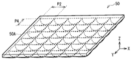
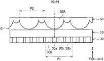
レンズシート50は、導光板10の上面から発せられた光(照明光)の発散角を狭めるものである。レンズシート50は、例えば、図1に示したように、レンズシート50の光入射面(下面)と、導光板10の光出射面(上面)との間にギャップGが形成されるように、導光板10の上に配置されている。ギャップGは、導光板10の光出射面(上面)の屈折率よりも低い屈折率の材料で充填された層であり、例えば、空気層である。なお、ギャップGが、常に空気層となっている必要はなく、例えば、導光板10の光出射面(上面)の屈折率よりも低い屈折率の材料からなる粘着剤もしくは接着剤で充填された層となっていてもよい。

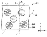
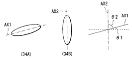
駆動回路60は、例えば、一の光変調セル30−1において微粒子34Bの光軸AX2がバルク34Aの光軸AX1と平行もしくはほぼ平行となり、他の光変調セル30−2において微粒子34Bの光軸AX2がバルク34Aの光軸AX1と交差もしくは直交するように各光変調セル30−1の一対の電極(部分電極32A、上側電極36)へ印加する電圧の大きさを制御するようになっている。つまり、駆動回路60は、電場制御によって、バルク34Aおよび微粒子34Bの光軸AX1,AX2の向きを互いに一致(もしくはほぼ一致)させたり、互いに異ならせたり(もしくは直交させたり)することができるようになっている。
[変形例1]
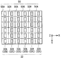
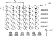
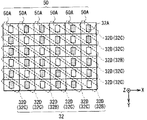
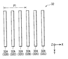
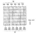
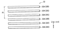
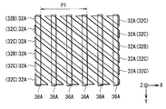
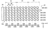
上記実施の形態では、各線状電極32Dが、光入射面10Aと平行な方向に延在している場合が例示されていたが、例えば、図27に示したように、複数の部分電極32Aのレイアウトが上記実施の形態と同一のままで、各線状電極32Dが光入射面10Aと斜めに交差する方向に延在していてもよい。このとき、P2=P1/N、P4=P3となっている場合には、例えば、図28Aに示したように、各凸部50Aが、1つの凸部50Aと1つの部分電極32Aとが1対1で対応するように配置されていることが好ましく、さらに、互いに対向するように配置されていることがより好ましい。なお、各凸部50Aが、図20Aでは矩形状となっていたが、例えば、図20Bに示したように、平行四辺形状、または菱形形状となっていてもよい。
また、上記実施の形態では、各部分電極32Aがブロック形状となっていたが、帯状の形状となっていてもよい。このとき、例えば、図31に示したように、各部分電極32Aが、光入射面10Aと平行な方向に延在しており、さらに、複数の部分電極32Aが、光入射面10Aと直交する方向に並んで配置されていてもよい。このとき、例えば、図32に示したように、複数の凸部50Aが、一列に並んで配置された複数の凸部50Aと、1つの部分電極32Aとが1対1で対応するように配置されていることが好ましい。
また、上記実施の形態および変形例1,2において、部分電極32A(または線状電極32D)の幅が狭くなっていてもよい。例えば、線状電極群が1つの線状電極32Bおよび3つの線状電極32Cで構成されている場合(三次元表示の際の視点数が4の場合)、部分電極32A(または線状電極32D)の幅が、P1/20(=P1×(1/4)×(1/5))以下となっていてもよい。このようにした場合には、照明装置1における発光線幅(散乱領域の幅)が狭くなる。その結果、照明装置1を表示装置のバックライトとして用いた場合に、三次元表示時に、表示装置の正面方向に形成される2重像を見えにくくすることができる。
また、上記実施の形態および変形例1〜3において、例えば、図37に示したように、互いに隣接する線状電極32B同士の間に、線状電極32Bの幅よりも広い幅の線状電極32Cが設けられていてもよい。
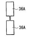
また、上記実施の形態および変形例1〜4では、上側電極36が面全体に形成されたシート状電極(ベタ膜)となっており、下側電極32が複数の部分電極32Aによって構成されていた。しかし、上側電極36が、例えば、図38に示したように、複数の部分電極36Aによって構成され、下側電極32が面全体に形成されたシート状電極(ベタ膜)となっていてもよい。この場合、各部分電極36Aは、各部分電極32Aと同様の構成となっている。
上記変形例5では、各線状電極36Dが、光入射面10Aと平行な方向に延在している場合が例示されていたが、例えば、図40に示したように、複数の部分電極36Aのレイアウトが上記変形例5と同一のままで、各線状電極36Dが光入射面10Aと斜めに交差する方向に延在していてもよい。このとき、P2=P1/Nとなっている場合には、各凸部50Aが、1つの凸部50Aと1つの部分電極32Aとが1対1で対応するように配置されていることが好ましく、さらに、互いに対向するように配置されていることがより好ましい。なお、各凸部50Aは、矩形状となっていてもよいし、平行四辺形状、または菱形形状となっていてもよい。
また、上記変形例5,6では、各部分電極36Aがブロック形状となっていたが、帯状の形状となっていてもよい。このとき、例えば、図42に示したように、各部分電極36Aが、光入射面10Aと平行な方向に延在しており、さらに、複数の部分電極36Aが、光入射面10Aと直交する方向に並んで配置されていてもよい。このとき、複数の凸部50Aが、一列に並んで配置された複数の凸部50Aと、1つの部分電極32Aとが1対1で対応するように配置されていることが好ましい。
また、上記変形例5〜7において、部分電極36A(または線状電極36D)の幅が狭くなっていてもよい。例えば、線状電極群が1つの線状電極36Bおよび3つの線状電極36Cで構成されている場合(三次元表示の際の視点数が4の場合)、部分電極36A(または線状電極36D)の幅が、P1/20(=P1×(1/4)×(1/5))以下となっていてもよい。このようにした場合には、照明装置1における発光線幅(散乱領域の幅)が狭くなる。その結果、照明装置1を表示装置のバックライトとして用いた場合に、三次元表示時に、表示装置の正面方向に形成される2重像を見えにくくすることができる。
また、上記変形例5〜8において、互いに隣接する線状電極36B同士の間に、線状電極36Bの幅よりも広い幅の線状電極36Cが設けられていてもよい。
また、上記実施の形態および上記変形例1〜9では、下側電極32および上側電極36のいずれか一方が複数の部分電極で構成されていたが、下側電極32および上側電極36の双方が複数の部分電極で構成されていてもよい。例えば、図45に示したように、下側電極32が帯状の複数の部分電極32Aによって構成され、上側電極36が帯状の複数の部分電極36Aによって構成されていてもよい。このとき、例えば、図45に示したように、部分電極32Aと部分電極36Aとが互いに対向していることが好ましい。さらに、下側電極32が複数の線状電極32B,32Cで構成されると共に、図46に示したように、上側電極36が、三次元表示時に部分駆動されず、一括駆動される複数の部分電極36Aで構成されていてもよい。また、上側電極36が複数の線状電極36B,36Cで構成されると共に、図47に示したように、下側電極32が、三次元表示時に部分駆動されず、一括駆動される複数の部分電極32Aで構成されていてもよい。
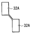
上記変形例2〜10において、線状電極32Dに含まれる各部分電極32Aは、互いに別個に形成されていてもよいし、例えば、図56A、図56Bに示したように、細線を介して互いに連結されていてもよい。線状電極32Dに含まれる各部分電極32Aが細線を介して互いに連結されている場合には、線状電極32Dは、いわゆるステップ状電極となっている。本変形例において、照明装置1は、各線状電極32Dに対応して、線状照明光、または、一列に並んだ複数の点状照明光(実質的には線状照明光)を出射するようになっている。
上記実施の形態および変形例1〜11では、光変調素子30は、導光板10の内部に空気層を介さずに密着して接合されていたが、例えば、図58に示したように、導光板10の上面に空気層を介さずに密着して接合されていてもよい。また、光変調素子30は、例えば、図59に示したように、導光板10の背後(下面)に空気層を介さずに密着して接合されていてもよい。
上記実施の形態および変形例1〜12では、下側電極32および上側電極36の辺部が直線状となっていたが、非直線状となっていてもよい。例えば、各部分電極36B,36Cにおいて、部分電極36Bのうち部分電極36Cと隣接する辺部が、凹凸形状となっていてもよい。同様に、各部分電極36B,36Cにおいて、部分電極36Cのうち部分電極36Bと隣接する辺部が、凹凸形状となっていてもよい。また、例えば、各部分電極32B,32Cにおいて、部分電極32Bのうち部分電極32Cと隣接する辺部が、凹凸形状となっていてもよい。同様に、各部分電極32B,32Cにおいて、部分電極32Cのうち部分電極32Bと隣接する辺部が、凹凸形状となっていてもよい。
上記実施の形態および変形例1〜13では、下側電極32および上側電極36には、その内部にパターニングが施されていなかったが、下側電極32および上側電極36の少なくとも一方の内部にパターニングが施されていてもよい。この場合に、下側電極32および上側電極36のうちパターニングされた電極のパターン密度が光源20からの距離に応じて異なっていてもよい。
上記実施の形態および変形例1〜14において、各部分電極32Aに対して、光源20からの距離に拘わらず同一の電圧が駆動回路60から印加されるようになっていてもよいし、光源20からの距離に応じた電圧が駆動回路60から印加されるようになっていてもよい。同様に、上記各実施の形態およびそれらの変形例において、各部分電極36Aに対して、光源20からの距離に拘わらず同一の電圧が駆動回路60から印加されるようになっていてもよいし、光源20からの距離に応じた電圧が駆動回路60から印加されるようになっていてもよい。
上記実施の形態および変形例1〜15において、例えば、各部分電極32Aが、さらに複数の微小電極によって構成されていてもよい。同様に、各部分電極36Aが、さらに複数の微小電極によって構成されていてもよい。
上記実施の形態および変形例1〜16において、駆動回路60は、散乱領域30Bを光入射面10Aと直交する方向に走査するように、下側電極32および上側電極36に電圧を印加するようにしてもよい。例えば、図68、図69、図70に順に示したように、駆動回路60による下側電極32および上側電極36への電圧印加により、散乱領域30Bを、光入射面10Aと直交する方向に遷移させることができる。
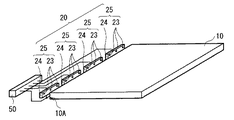
上記実施の形態および変形例1〜17において、光源20は、例えば、図71Aに示したように、線状光源21と、反射ミラー22とにより構成されていてもよい。線状光源21は、例えば、HCFL、またはCCFLからなる。反射ミラー22は、線状光源21から発せられた光のうち光入射面10Aに直接入射しない方向に向かう光を光入射面10A側に反射するものである。光源20は、例えば、図71Bまたは図71Cに示したように、複数の点状光源23を一列に配置して構成されたものであってもよい。各点状光源23は、光入射面10Aに向かって光を射出するようになっており、例えば、光入射面10Aとの対向面に発光スポットを有する発光素子からなる。そのような発光素子としては、例えば、LED、または、レーザダイオード(LD;Laser Diode)などが挙げられる。効率、薄型化、均一性の観点からは、各点状光源23がホワイトLEDであることが好ましい。なお、光源20に含まれる複数の点状光源23が、例えば、赤色LED、緑色LEDおよび青色LEDを含んで構成されていてもよい。
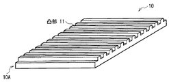
上記実施の形態および変形例1〜18において、導光板10が、例えば、図72Aに示したように、帯状の複数の凸部11を上面に有していてもよい。なお、導光板10は、例えば、図72Bに示したように、帯状の複数の凸部11を下面に有していてもよい。また、導光板10は、例えば、図示しないが、帯状の複数の凸部11を導光板10の内部に有していてもよい。また、導光板10の内部が空洞状になっていてもよいし、密に充填されていてもよい。
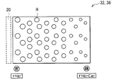
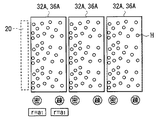
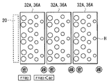
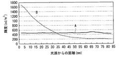
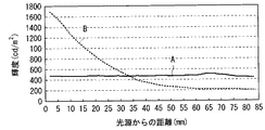
上記変形例19において、光源20が、例えば、図71Bまたは図71Cに示したように、複数の光源ブロック25を一列に配置して構成されたものであってもよい。この場合に、互いに隣接する2つの光源ブロック25の間隙が広くなっているときには、開口Hの、単位面積あたりの密度が、光入射面10Aと平行な方向において、光源ブロック25寄りの箇所で相対的に大きく、光源ブロック25から離れた箇所で相対的に小さくなっていてもよい。例えば、図75、図77に示したように、開口H(半径一定)の、単位面積あたりの数が、光入射面10Aと平行な方向において、光源ブロック25寄りの箇所で相対的に多く、光源ブロック25から離れた箇所で相対的に少なくなっていてもよい。また、例えば、図76、図78に示したように、開口Hの半径が、光入射面10Aと平行な方向において、光源ブロック25寄りの箇所で相対的に大きく、光源ブロック25から離れた箇所で相対的に小さくなっていてもよい。このようにした場合には、光入射面10Aと平行な方向において、光源ブロック25寄りの輝度を、開口Hを設けていない場合よりも低く抑え、かつ光源ブロック21から離れた箇所の輝度を、開口Hを設けていない場合よりも高くすることができる。その結果、例えば、照明装置1の光射出領域全体を明状態とした場合に、面内輝度を均一化することができる。例えば、光入射面10Aから2mm離れた箇所でのパターニング密度が図91のAに示したような分布となっている場合には、図80のAに示したように、光入射面10Aと平行な方向において、面内輝度を均一化することができる。一方、例えば、光入射面10Aから2mm離れた箇所でのパターニング密度が図79のBに示したような平坦な分布となっている場合には、図80のBに示したように、光入射面10Aと平行な方向において、面内輝度が大きく変化してしまう。なお、本変形例において、光源ブロック25の代わりに、点状光源23が用いられている場合には、開口Hの、単位面積あたりの密度が、光入射面10Aと平行な方向において、点状光源23寄りの箇所で相対的に大きく、点状光源23から離れた箇所で相対的に小さくなっていてもよい。このようにした場合にも、光入射面10Aと平行な方向において、面内輝度を均一化することができる。
上記実施の形態および変形例1〜20において、各線状電極32Dが、面内の一の方向(光入射面10Aに平行な方向)に延在している場合に、線状電極32Bの幅W1および線状電極32Cの幅W3が、光源20からの距離に応じて異なっていてもよい。例えば、図81に示したように、線状電極32Bの幅W1および線状電極32Cの幅W3が、光源20寄りの箇所で相対的に小さく、光源20から離れた箇所で相対的に大きくなっていてもよい。このようにした場合には、例えば、照明装置1の光射出領域全体を明状態とした場合に、面内輝度を均一化することができる。また、例えば、光入射面10Aと直交する方向において、光源20に近い領域と、光源20から遠い領域とにおいて白表示をしたときに、双方の領域の白輝度を等しくすることが可能となる。なお、図81には、各線状電極群において、線状電極32B,32Cの幅W1,W3(X軸方向の幅)が光源20からの距離に応じて異なっている場合が例示されている。図示しないが、各線状電極群において、線状電極32B,32CのY軸方向の幅が光源20からの距離に応じて異なっていてもよく、線状電極32B,32CのX軸方向の幅とY軸方向の幅の両方が光源20からの距離に応じて異なっていてもよい 。
また、上記実施の形態および変形例1〜21において、透明基板31および透明基板37のうち少なくとも一方が、導光板10と一体に形成されたものであってもよい。例えば、上記各実施の形態、第1変形例および第2変形例において、透明基板37が導光板10と接している場合には、例えば、図88に示したように、透明基板37が導光板10と一体に形成されていてもよい。このとき、透明基板37は、本技術の「第1基板」または「第2基板」の一具体例に相当する。また、例えば、上記実施の形態および変形例1〜21において、透明基板31が導光板10と接している場合には、例えば、図89に示したように、透明基板31が導光板10と一体に形成されていてもよい。このとき、透明基板31は、本技術の「第1基板」または「第2基板」の一具体例に相当する。また、例えば、上記各実施の形態および変形例1〜21において、透明基板31,37がともに導光板10と接している場合には、例えば、図90に示したように、透明基板31,37が導光板10と一体に形成されていてもよい。このとき、透明基板31または透明基板37が、本技術の「第1基板」または「第2基板」の一具体例に相当する。
また、上記各実施の形態および変形例1〜22において、反射板40の代わりに、光反射抑制層が設けられていてもよい。光反射抑制層は、例えば、低反射率材料が基材の表面に塗布されたものであってもよいし、光を吸収する材料が基材の表面に塗布されたものであってもよい。例えば、図91に示したように、反射板40の代わりに、光反射抑制層90が設けられていてもよい。光反射抑制層90は、例えば、低反射率材料が基材の表面に塗布されたもの、または、光を吸収する材料が基材の表面に塗布されたものからなる。このように、光反射抑制層90を設けることにより、反射板40を設けたときに反射板40で反射された光が透過領域30Aを透過して表示パネル210に入射する割合を低く抑えることができる。その結果、コントラストを上げることができる。
また、上記各実施の形態および変形例1〜23において、配向膜33,35として水平配向膜が用いられていたが、垂直配向膜が用いられていてもよい。ただし、その場合には、微粒子34B内に含まれる液晶分子として、負の誘電率異方性を有するもの(いわゆるネガ型液晶)を用いることが好ましい。
また、上記実施の形態および変形例1〜24において、光変調層34との関係で光出射面1A側に配置された透明部材(透明基板37および導光板10)の厚さを薄くしてもよい。このようにした場合には、集光率が低下するので、照明装置1における発光線幅(散乱領域の幅)が狭くなる。その結果、照明装置1を表示装置のバックライトとして用いた場合に、三次元表示時に、表示装置の正面方向に形成される2重像を見えにくくすることができる。また、集光率の低下により、三次元表示の際の視差方向の視野角がレンズシート50によってあまり狭まらず、実用に耐え得る十分な大きさとすることができる。
上記実施の形態および変形例1〜25に係る照明装置1を備えた、テレビ放送信号の受送信システムについて説明する。
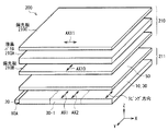
図93は、受信側装置200の構成例を示すブロック図である。受信側装置200は、例えば、上記の有線や無線に接続可能なテレビジョンである。受信側装置200は、例えば、アンテナ端子201、デジタルチューナ202、デマルチプレクサ203、演算回路204、およびメモリ205を有している。受信側装置200は、また、例えば、デコーダ206、映像信号処理回路207、グラフィック生成回路208、パネル駆動回路209、表示パネル210、バックライト211、音声信号処理回路212、音声増幅回路213、およびスピーカ214を有している。受信側装置200は、さらに、例えば、リモコン受信回路215、およびリモコン送信機216を有している。
図94は、受信側装置200における表示部の断面構成の一例を表したものである。なお、図94は、模式的に表したものであり、実際の寸法や形状と同一であるとは限らない。受信側装置200は、表示パネル210と、表示パネル210の背後に配置されたバックライト211とを備えている。
[変形例1]
上記第2の実施の形態において、レンズシート50が、粘着剤もしくは接着剤を用いて、偏光板210Bに固定されていてもよい。このとき、例えば、図99に示したように、レンズシート50の平坦面が、粘着剤もしくは接着剤からなる固定層212を介して偏光板210Bに固定されていることが好ましい。また、凸部50AがUV硬化樹脂などのエネルギー硬化性樹脂を固化させることにより形成されたものである場合には、例えば、図100に示したように、複数の凸部50Aが偏光板210Bの表面に直接、形成されていてもよい。
上記第2の実施の形態およびその変形例において、例えば、図101、図102に示したように、バックライト211の光射出側に、パララックスバリア80が設けられていてもよい。パララックスバリア80は、図101に示したように、レンズシート50の上に設けられていることが好ましい。この場合、バックライト211から出力された光の発散角を狭めることができるので、パララックスバリア80の光透過部分に入射する光の量が増加し、高い輝度を得るができる。パララックスバリア80が、レンズシート50の上に設けられている場合は、レンズシート50が、粘着剤もしくは接着剤を用いて、パララックスバリア80の偏光板81に固定されていてもよい。また、レンズシート50の複数の凸部50Aがパララックスバリア80の偏光板81の表面に直接、形成されていてもよい。
上記第2の実施の形態およびその変形例において、三次元表示のときには、例えば、図105Aの太枠で示したように、表示パネル210の4つの画素210−1〜210−4が1つの三次元用画素210Dとして駆動される。このとき、バックライト211は、例えば、図105Bに示したように、三次元用画素210Dごとに1つずつ散乱領域30Bを形成し、各画素210−1〜210−4に、互いに異なる入射角でバックライト光を入射させる。これにより、各三次元用画素210D内の共通の位置にある画素(例えば、図97では、210−1,210−2,210−3または210−4)には、各帯状照明光が略同一の角度で入射する。その結果、各三次元用画素210D内の共通の位置にある画素からは、その画素によって変調された映像光が所定の角度で出力される。このとき、観察者は、例えば、図105Cに示した画素210aからの映像光を右目で観察すると同時に、図105Dに示した画素210aからの映像光を左目で観察することになる。つまり、観察者は、左右の目で、互いに異なる視差の映像を観察することになる。その結果、観察者は、表示パネル210に三次元映像(立体映像)が表示されていると認識する。
また、上記第2の実施の形態およびその変形例において、表示パネル210を駆動する駆動回路(図示せず)は、表示パネル210を時分割に駆動するようにしてもよい。この場合に、駆動回路50は、所定の周期内において、表示パネル210の表示が、視差の数と等しい数の画素行内で1画素行ずつ順次切り換わるのと同期して、バックライト211からの帯状照明光の出力箇所を切り替える。例えば、視点数4の場合、図108、図109、図110、図111に順に示したように、駆動回路50は、1フレーム期間(1/60秒)内において、表示パネル210の表示が、4画素行内で1画素行ずつ順次切り換わるのと同期して、バックライト211からの帯状照明光の出力箇所を切り替える。このとき、表示パネル210を駆動する駆動回路(図示せず)は、1フレーム期間(1/60秒)内において、表示パネル210の表示が、視差の数と等しい数の画素行内で1画素行ずつ順次切り換わるように、各画素に対して映像信号に対応する電圧を印加する。このように、切り替えを高速に行うことにより、観察者は、瞬間に光っている画素数の4倍の画素を知覚するようになり、実質的な解像度をあげることができる。
また、上記第2の実施の形態およびその変形例において、例えば、図112、図113に示したように、バックライト211の光軸AX1と、偏光板210Bの透過軸AX10とが互いに直交または交差する方向を向いていてもよい。ただし、その場合には、送信側装置100は、バックライト211と、偏光板210Bとの間に、光軸AX1と透過軸AX10とがなす角の二等分線と平行な方向に光軸AX12を有する1/2λ板217を備えていることが好ましい。このようにした場合には、1/2λ板217によって、バックライト211から出射された偏光光の偏光方向を、透過軸AX10と平行な方向に回転させることができる。その結果、光の利用効率を高くすることができる。
次に、上記各実施の形態に係る照明装置1の実施例について、比較例と対比しつつ説明する。実施例1〜7、比較例1,2の構成を、以下の表1にまとめた。
実施例7では、比較例2に比べて、レンズシートの効果により、正面輝度が3D表示で140%、2D表示で151%の輝度上昇を確認した。
(1)
照明光を出力可能な照明装置と、映像信号に応じて前記照明光を変調することにより映像光を生成する表示パネルとを備えた表示装置に用いられる前記照明装置において、
前記照明光を生成する照明光学系と、
前記照明光の発散角を狭める複数のレンズと
を備え、
前記照明光学系は、
離間して互いに対向配置された第1基板および第2基板と、
前記第1基板または前記第2基板の端面に光を照射する光源と、
前記第1基板および前記第2基板の間隙に設けられ、かつ電場の大きさに応じて、前記光源からの光に対して散乱性もしくは透明性を示す光変調層と、
三次元表示モードのときに、前記光変調層に複数の線状散乱領域、または複数列に並んだ複数の点状散乱領域を生成させる電場を発生させ、二次元表示モードのときに、前記光変調層に面状散乱領域、またはマトリクス状に並んだ複数の点状散乱領域を生成させる電場を発生させる電極と
を有し、
前記複数のレンズは、前記線状散乱領域の延在方向、または一列に並んだ複数の点状散乱領域の並び方向に並んで配置されるとともに、前記線状散乱領域の延在方向、または一列に並んだ複数の点状散乱領域の並び方向と交差する方向に並んで配置されている
照明装置。
(2)
前記レンズは、当該レンズの光入射面または光出射面に曲面を含んで構成されている
(1)に記載の照明装置。
(3)
前記レンズは、凸形状となっており、当該レンズの頂点位置が前記線状散乱領域、または一列に並んだ複数の点状散乱領域と対向するように配置されている
請求項2に記載の照明装置。
(1)または(2)に記載の照明装置。
(4)
前記レンズのピッチは、前記線状散乱領域、または一列に並んだ複数の点状散乱領域のピッチをP1とすると、P1/n(nは三次元表示モードのときの視点数)となっている
(3)に記載の照明装置。
(5)
前記電極は、三次元表示モードのときに、前記光変調層に、複数列に並んだ複数の点状散乱領域を生成させる電場を発生させるようになっており、
各レンズは、1つのレンズと1つの点状散乱領域とが1対1で対応するように配置されている
(3)または(4)に記載の照明装置。
(6)
前記電極は、二次元表示モードのときに、前記光変調層に、マトリクス状に並んだ複数の点状散乱領域を生成させる電場を発生させるようになっており、
各レンズは、1つのレンズと1つの点状散乱領域とが1対1で対応するように配置されている
(3)ないし(5)のいずれか1つに記載の照明装置。
(7)
前記レンズは、屈折率が等方性の材料で構成されている
(1)ないし(6)のいずれか1つに記載の照明装置。
(8)
前記レンズは、前記光変調層側に突出している
(3)ないし(7)のいずれか1つに記載の照明装置。
(9)
前記表示パネルは、偏光板を有し、
前記複数のレンズは、前記偏光板に接着されている
(8)に記載の照明装置。
(10)
照明光を出力可能な照明装置と、
映像信号に応じて前記照明光を変調することにより映像光を生成する表示パネルと
を備え、
前記照明装置は、
前記照明光を生成する照明光学系と、
前記照明光の発散角を狭める複数のレンズと
を有し、
前記照明光学系は、
離間して互いに対向配置された第1基板および第2基板と、
前記第1基板または前記第2基板の端面に光を照射する光源と、
前記第1基板および前記第2基板の間隙に設けられ、かつ電場の大きさに応じて、前記光源からの光に対して散乱性もしくは透明性を示す光変調層と、
三次元表示モードのときに、前記光変調層に複数の線状散乱領域、または複数列に並んだ複数の点状散乱領域を生成させる電場を発生させ、二次元表示モードのときに、前記光変調層に面状散乱領域、またはマトリクス状に並んだ複数の点状散乱領域を生成させる電場を発生させる電極と
を有し、
前記複数のレンズは、前記線状散乱領域の延在方向、または一列に並んだ複数の点状散乱領域の並び方向に並んで配置されるとともに、前記線状散乱領域の延在方向、または一列に並んだ複数の点状散乱領域の並び方向と交差する方向に並んで配置されている
表示装置。
Claims (9)
- 照明光を出力可能な照明装置と、映像信号に応じて前記照明光を変調することにより映像光を生成する表示パネルとを備えた表示装置に用いられる前記照明装置において、
前記照明光を生成する照明光学系と、
前記照明光の発散角を狭める複数のレンズと
を備え、
前記照明光学系は、
離間して互いに対向配置された第1基板および第2基板と、
前記第1基板または前記第2基板の端面に光を照射する光源と、
前記第1基板および前記第2基板の間隙に設けられ、かつ電場の大きさに応じて、前記光源からの光に対して散乱性もしくは透明性を示す光変調層と、
三次元表示モードのときに、前記光変調層に複数の線状散乱領域、または複数列に並んだ複数の点状散乱領域を生成させる電場を発生させ、二次元表示モードのときに、前記光変調層に面状散乱領域、または前記三次元表示モードのときの前記複数の点状散乱領域の列間のピッチよりも狭いピッチでマトリクス状に並んだ複数の点状散乱領域を生成させる電場を発生させる電極と
を有し、
前記複数のレンズは、前記線状散乱領域の延在方向、または一列に並んだ複数の点状散乱領域の並び方向に並んで配置されるとともに、前記線状散乱領域の延在方向、または一列に並んだ複数の点状散乱領域の並び方向と交差する方向に並んで配置されており、
前記レンズは、凸形状となっており、当該レンズの頂点位置が前記線状散乱領域、または一列に並んだ複数の点状散乱領域と対向するように配置されている
照明装置。 - 前記レンズは、当該レンズの光入射面または光出射面に曲面を含んで構成されている
請求項1に記載の照明装置。 - 前記レンズのピッチは、前記線状散乱領域、または一列に並んだ複数の点状散乱領域のピッチをP1とすると、P1/n(nは三次元表示モードのときの視点数)となっている
請求項1または請求項2に記載の照明装置。 - 前記電極は、三次元表示モードのときに、前記光変調層に、複数列に並んだ複数の点状散乱領域を生成させる電場を発生させるようになっており、
各レンズは、1つのレンズと1つの点状散乱領域とが1対1で対応するように配置されている
請求項1ないし請求項3のいずれか一項に記載の照明装置。 - 前記電極は、二次元表示モードのときに、前記光変調層に、マトリクス状に並んだ複数の点状散乱領域を生成させる電場を発生させるようになっており、
各レンズは、1つのレンズと1つの点状散乱領域とが1対1で対応するように配置されている
請求項1ないし請求項4のいずれか一項に記載の照明装置。 - 前記レンズは、屈折率が等方性の材料で構成されている
請求項1ないし請求項5のいずれか一項に記載の照明装置。 - 前記レンズは、前記光変調層側に突出している
請求項1ないし請求項6のいずれか一項に記載の照明装置。 - 前記表示パネルは、偏光板を有し、
前記複数のレンズは、前記偏光板に固定されている
請求項7に記載の照明装置。 - 照明光を出力可能な照明装置と、
映像信号に応じて前記照明光を変調することにより映像光を生成する表示パネルと
を備え、
前記照明装置は、
前記照明光を生成する照明光学系と、
前記照明光の発散角を狭める複数のレンズと
を有し、
前記照明光学系は、
離間して互いに対向配置された第1基板および第2基板と、
前記第1基板または前記第2基板の端面に光を照射する光源と、
前記第1基板および前記第2基板の間隙に設けられ、かつ電場の大きさに応じて、前記
光源からの光に対して散乱性もしくは透明性を示す光変調層と、
三次元表示モードのときに、前記光変調層に複数の線状散乱領域、または複数列に並んだ複数の点状散乱領域を生成させる電場を発生させ、二次元表示モードのときに、前記光変調層に面状散乱領域、または前記三次元表示モードのときの前記複数の点状散乱領域の列間のピッチよりも狭いピッチでマトリクス状に並んだ複数の点状散乱領域を生成させる電場を発生させる電極と
を有し、
前記複数のレンズは、前記線状散乱領域の延在方向、または一列に並んだ複数の点状散乱領域の並び方向に並んで配置されるとともに、前記線状散乱領域の延在方向、または一列に並んだ複数の点状散乱領域の並び方向と交差する方向に並んで配置されており、
前記レンズは、凸形状となっており、当該レンズの頂点位置が前記線状散乱領域、または一列に並んだ複数の点状散乱領域と対向するように配置されている
表示装置。
Priority Applications (6)
| Application Number | Priority Date | Filing Date | Title |
|---|---|---|---|
| JP2012176490A JP6098064B2 (ja) | 2012-08-08 | 2012-08-08 | 表示装置および照明装置 |
| TW102124780A TWI550307B (zh) | 2012-08-08 | 2013-07-10 | A display device and a lighting device |
| US14/418,769 US9785006B2 (en) | 2012-08-08 | 2013-07-25 | Display apparatus and illumination unit |
| PCT/JP2013/070130 WO2014024688A1 (ja) | 2012-08-08 | 2013-07-25 | 表示装置および照明装置 |
| EP13828432.8A EP2884332B1 (en) | 2012-08-08 | 2013-07-25 | Display apparatus and illuminating apparatus |
| CN201380040718.7A CN104508546B (zh) | 2012-08-08 | 2013-07-25 | 显示装置及照明单元 |
Applications Claiming Priority (1)
| Application Number | Priority Date | Filing Date | Title |
|---|---|---|---|
| JP2012176490A JP6098064B2 (ja) | 2012-08-08 | 2012-08-08 | 表示装置および照明装置 |
Publications (3)
| Publication Number | Publication Date |
|---|---|
| JP2014035448A JP2014035448A (ja) | 2014-02-24 |
| JP2014035448A5 JP2014035448A5 (ja) | 2015-08-20 |
| JP6098064B2 true JP6098064B2 (ja) | 2017-03-22 |
Family
ID=50067921
Family Applications (1)
| Application Number | Title | Priority Date | Filing Date |
|---|---|---|---|
| JP2012176490A Expired - Fee Related JP6098064B2 (ja) | 2012-08-08 | 2012-08-08 | 表示装置および照明装置 |
Country Status (6)
| Country | Link |
|---|---|
| US (1) | US9785006B2 (ja) |
| EP (1) | EP2884332B1 (ja) |
| JP (1) | JP6098064B2 (ja) |
| CN (1) | CN104508546B (ja) |
| TW (1) | TWI550307B (ja) |
| WO (1) | WO2014024688A1 (ja) |
Families Citing this family (37)
| Publication number | Priority date | Publication date | Assignee | Title |
|---|---|---|---|---|
| TW201400946A (zh) * | 2012-05-09 | 2014-01-01 | Sony Corp | 照明裝置及顯示裝置 |
| US9568772B2 (en) * | 2012-09-14 | 2017-02-14 | Apple Inc. | Displays with elevated backlight efficiency |
| KR102155703B1 (ko) * | 2014-01-03 | 2020-09-14 | 삼성전자주식회사 | 디스플레이 장치 |
| JP6336625B2 (ja) | 2014-02-17 | 2018-06-06 | ジオプティカ・ゲゼルシャフト・ミット・ベシュレンクテル・ハフツングSioptica Gmbh | 切り換え可能な照明デバイス及びその使用 |
| TWI599818B (zh) | 2014-10-22 | 2017-09-21 | 日本顯示器股份有限公司 | 顯示裝置 |
| KR20160087021A (ko) * | 2015-01-12 | 2016-07-21 | 삼성디스플레이 주식회사 | 표시 장치 |
| TWI607233B (zh) | 2015-02-16 | 2017-12-01 | 財團法人工業技術研究院 | 光學膜結構與顯示器結構 |
| KR102309921B1 (ko) * | 2015-03-16 | 2021-10-07 | 삼성디스플레이 주식회사 | 표시 장치 및 이에 포함되는 광학 필름 |
| JP6588263B2 (ja) | 2015-07-16 | 2019-10-09 | デクセリアルズ株式会社 | 拡散板、表示装置、投影装置及び照明装置 |
| KR102447099B1 (ko) | 2015-09-23 | 2022-09-26 | 삼성전자주식회사 | 광원 디바이스, 이를 포함하는 디스플레이 장치, 디스플레이 방법 |
| JP6671940B2 (ja) | 2015-12-07 | 2020-03-25 | 株式会社ジャパンディスプレイ | 表示装置 |
| JP6319355B2 (ja) * | 2016-02-23 | 2018-05-09 | 株式会社デンソー | ヘッドアップディスプレイ装置 |
| US10466538B2 (en) | 2016-03-15 | 2019-11-05 | Japan Display Inc. | Display device |
| KR102554120B1 (ko) * | 2016-03-24 | 2023-07-12 | 티씨엘 차이나 스타 옵토일렉트로닉스 테크놀로지 컴퍼니 리미티드 | 액정 표시 장치 |
| JP6716323B2 (ja) * | 2016-04-01 | 2020-07-01 | 株式会社ジャパンディスプレイ | 表示装置 |
| CN105974672B (zh) * | 2016-07-27 | 2019-03-12 | 京东方科技集团股份有限公司 | 一种显示装置 |
| JP6877910B2 (ja) | 2016-08-01 | 2021-05-26 | 株式会社ジャパンディスプレイ | 表示装置 |
| KR20180036881A (ko) * | 2016-09-30 | 2018-04-10 | 삼성디스플레이 주식회사 | 백라이트 유닛 및 그것을 포함하는 표시 장치 |
| KR102698292B1 (ko) | 2016-11-10 | 2024-08-23 | 삼성전자주식회사 | 액정 광 편향기 및 디스플레이 장치 |
| CN106647048B (zh) * | 2017-03-20 | 2019-07-16 | 京东方科技集团股份有限公司 | 光学结构、显示装置及其工作方法 |
| US10670778B2 (en) * | 2017-07-20 | 2020-06-02 | Htc Corporation | Optical lens, optical system and method of manufacturing optical lens |
| JP7005243B2 (ja) | 2017-09-14 | 2022-01-21 | 株式会社ジャパンディスプレイ | 表示装置 |
| WO2019181404A1 (ja) * | 2018-03-20 | 2019-09-26 | ソニー株式会社 | 画像表示装置 |
| JP7160313B2 (ja) | 2018-07-23 | 2022-10-25 | 株式会社ジャパンディスプレイ | 表示装置 |
| CN111090191B (zh) | 2018-10-24 | 2022-10-04 | 中强光电股份有限公司 | 光源模块及双屏幕显示装置 |
| KR102695173B1 (ko) | 2018-12-13 | 2024-08-19 | 삼성디스플레이 주식회사 | 표시모듈 및 이를 포함하는 헤드 마운트 표시장치 |
| CN109616019B (zh) * | 2019-01-18 | 2021-05-18 | 京东方科技集团股份有限公司 | 显示面板、显示装置、三维显示方法和三维显示系统 |
| CN110133894B (zh) * | 2019-05-31 | 2022-01-11 | 京东方科技集团股份有限公司 | 透明显示面板及其制备方法、透明显示器 |
| USD932141S1 (en) * | 2019-09-09 | 2021-10-05 | Debra Ansell | Garment with detachable illumination strip |
| USD933335S1 (en) * | 2019-09-09 | 2021-10-19 | Debra Ansell | Modular programmable illumination unit for a wearable article |
| CN110596800B (zh) * | 2019-09-29 | 2022-02-15 | 重庆京东方显示照明有限公司 | 用于光扩散膜的基膜、光扩散膜、显示装置及其制备方法 |
| WO2021085682A1 (ko) * | 2019-10-31 | 2021-05-06 | 엘지전자 주식회사 | 디스플레이 장치 |
| DE102020002323B3 (de) * | 2020-04-07 | 2021-07-22 | Sioptica Gmbh | Optisches Element zur Beeinflussung von Lichtrichtungen und Bildschirm mit einem solchen optischen Element |
| CN115348436B (zh) * | 2021-05-13 | 2023-08-25 | 幻景启动股份有限公司 | 可降低格栅感的立体图像显示装置 |
| TWI786775B (zh) | 2021-08-19 | 2022-12-11 | 友達光電股份有限公司 | 顯示裝置 |
| CN116699875A (zh) * | 2022-02-25 | 2023-09-05 | 群创光电股份有限公司 | 光学结构 |
| TWI889229B (zh) * | 2024-03-07 | 2025-07-01 | 達擎股份有限公司 | 可調變透明顯示器 |
Family Cites Families (24)
| Publication number | Priority date | Publication date | Assignee | Title |
|---|---|---|---|---|
| US6137456A (en) * | 1996-07-01 | 2000-10-24 | Corning Incorporated | Electronic display device for simultaneously displaying 2D and 3D images |
| GB0326005D0 (en) * | 2003-11-07 | 2003-12-10 | Koninkl Philips Electronics Nv | Waveguide for autostereoscopic display |
| GB0328005D0 (en) * | 2003-12-03 | 2004-01-07 | Koninkl Philips Electronics Nv | 2D/3D Displays |
| JP2006010868A (ja) * | 2004-06-23 | 2006-01-12 | Sony Corp | マイクロレンズアレイ、液晶表示装置、投射型表示装置 |
| KR101419234B1 (ko) * | 2007-12-18 | 2014-07-15 | 엘지디스플레이 주식회사 | 액정 전계 렌즈 및 이를 이용한 입체 표시 장치 |
| JP4582223B2 (ja) * | 2008-08-12 | 2010-11-17 | ソニー株式会社 | 照明装置および表示装置 |
| JP5263593B2 (ja) * | 2008-10-07 | 2013-08-14 | ソニー株式会社 | 照明装置および表示装置 |
| JP5315963B2 (ja) * | 2008-12-11 | 2013-10-16 | 凸版印刷株式会社 | 光拡散デバイス、バックライトユニットおよびディスプレイ装置 |
| JP2011029146A (ja) * | 2009-06-26 | 2011-02-10 | Sony Corp | バックライト、および液晶表示装置 |
| TWI417574B (zh) * | 2009-10-09 | 2013-12-01 | Chunghwa Picture Tubes Ltd | 變焦透鏡陣列與可切換式平面立體顯示器 |
| JP5526763B2 (ja) * | 2009-12-24 | 2014-06-18 | 凸版印刷株式会社 | 隠蔽構造体を備えた照明装置と表示装置 |
| JP5467388B2 (ja) | 2010-04-06 | 2014-04-09 | ソニー株式会社 | 照明装置および表示装置 |
| JP2011222237A (ja) * | 2010-04-07 | 2011-11-04 | Sony Corp | 照明装置および表示装置 |
| JP5679308B2 (ja) * | 2010-04-07 | 2015-03-04 | ソニー株式会社 | 照明装置および表示装置 |
| KR101783975B1 (ko) * | 2010-07-14 | 2017-10-11 | 삼성디스플레이 주식회사 | 입체 영상 표시 장치 |
| CN102156353B (zh) * | 2010-10-15 | 2012-06-27 | 深圳超多维光电子有限公司 | 二维/三维可转换显示装置、显示方法、个人数字助理及电脑 |
| JP5516319B2 (ja) * | 2010-10-20 | 2014-06-11 | ソニー株式会社 | 照明装置および表示装置 |
| JP2012104375A (ja) * | 2010-11-10 | 2012-05-31 | Toshiba Corp | 表示装置およびバックライト装置 |
| US8730416B2 (en) * | 2010-12-17 | 2014-05-20 | Semiconductor Energy Laboratory Co., Ltd. | Liquid crystal display device |
| KR20120069432A (ko) * | 2010-12-20 | 2012-06-28 | 삼성전자주식회사 | 입체영상표시장치 및 그 구동 방법 |
| JP2012234725A (ja) * | 2011-05-02 | 2012-11-29 | Sony Corp | 表示装置および照明装置 |
| JP2013050694A (ja) * | 2011-07-29 | 2013-03-14 | Sony Corp | 照明装置および表示装置 |
| JP5991053B2 (ja) | 2011-10-04 | 2016-09-14 | ソニー株式会社 | 表示装置および照明装置 |
| JP6035866B2 (ja) * | 2012-05-22 | 2016-11-30 | ソニー株式会社 | 照明装置および表示装置 |
-
2012
- 2012-08-08 JP JP2012176490A patent/JP6098064B2/ja not_active Expired - Fee Related
-
2013
- 2013-07-10 TW TW102124780A patent/TWI550307B/zh not_active IP Right Cessation
- 2013-07-25 CN CN201380040718.7A patent/CN104508546B/zh not_active Expired - Fee Related
- 2013-07-25 EP EP13828432.8A patent/EP2884332B1/en not_active Not-in-force
- 2013-07-25 WO PCT/JP2013/070130 patent/WO2014024688A1/ja not_active Ceased
- 2013-07-25 US US14/418,769 patent/US9785006B2/en not_active Expired - Fee Related
Also Published As
| Publication number | Publication date |
|---|---|
| CN104508546A (zh) | 2015-04-08 |
| TW201407196A (zh) | 2014-02-16 |
| WO2014024688A1 (ja) | 2014-02-13 |
| EP2884332B1 (en) | 2019-07-03 |
| US9785006B2 (en) | 2017-10-10 |
| JP2014035448A (ja) | 2014-02-24 |
| CN104508546B (zh) | 2017-05-31 |
| EP2884332A1 (en) | 2015-06-17 |
| TWI550307B (zh) | 2016-09-21 |
| US20150293402A1 (en) | 2015-10-15 |
| EP2884332A4 (en) | 2016-06-22 |
Similar Documents
| Publication | Publication Date | Title |
|---|---|---|
| JP6098064B2 (ja) | 表示装置および照明装置 | |
| JP5991053B2 (ja) | 表示装置および照明装置 | |
| TWI477818B (zh) | Lighting device and display device | |
| JP5906649B2 (ja) | 表示装置 | |
| JP5699786B2 (ja) | 表示装置および照明装置 | |
| JP5929083B2 (ja) | 表示装置 | |
| JP5948813B2 (ja) | 照明装置および表示装置 | |
| US9223160B2 (en) | Display | |
| JP2011222237A (ja) | 照明装置および表示装置 | |
| JP2013050694A (ja) | 照明装置および表示装置 |
Legal Events
| Date | Code | Title | Description |
|---|---|---|---|
| A521 | Request for written amendment filed |
Free format text: JAPANESE INTERMEDIATE CODE: A523 Effective date: 20150702 |
|
| A621 | Written request for application examination |
Free format text: JAPANESE INTERMEDIATE CODE: A621 Effective date: 20150702 |
|
| A131 | Notification of reasons for refusal |
Free format text: JAPANESE INTERMEDIATE CODE: A131 Effective date: 20160719 |
|
| A521 | Request for written amendment filed |
Free format text: JAPANESE INTERMEDIATE CODE: A523 Effective date: 20160817 |
|
| TRDD | Decision of grant or rejection written | ||
| A01 | Written decision to grant a patent or to grant a registration (utility model) |
Free format text: JAPANESE INTERMEDIATE CODE: A01 Effective date: 20170124 |
|
| A61 | First payment of annual fees (during grant procedure) |
Free format text: JAPANESE INTERMEDIATE CODE: A61 Effective date: 20170206 |
|
| R151 | Written notification of patent or utility model registration |
Ref document number: 6098064 Country of ref document: JP Free format text: JAPANESE INTERMEDIATE CODE: R151 |
|
| R250 | Receipt of annual fees |
Free format text: JAPANESE INTERMEDIATE CODE: R250 |
|
| LAPS | Cancellation because of no payment of annual fees |