JP6147977B2 - Led照明器具およびledユニット - Google Patents
Led照明器具およびledユニット Download PDFInfo
- Publication number
- JP6147977B2 JP6147977B2 JP2012211724A JP2012211724A JP6147977B2 JP 6147977 B2 JP6147977 B2 JP 6147977B2 JP 2012211724 A JP2012211724 A JP 2012211724A JP 2012211724 A JP2012211724 A JP 2012211724A JP 6147977 B2 JP6147977 B2 JP 6147977B2
- Authority
- JP
- Japan
- Prior art keywords
- led
- led lighting
- lighting apparatus
- substrate
- protective layer
- Prior art date
- Legal status (The legal status is an assumption and is not a legal conclusion. Google has not performed a legal analysis and makes no representation as to the accuracy of the status listed.)
- Expired - Fee Related
Links
Images





Classifications
-
- F—MECHANICAL ENGINEERING; LIGHTING; HEATING; WEAPONS; BLASTING
- F21—LIGHTING
- F21K—NON-ELECTRIC LIGHT SOURCES USING LUMINESCENCE; LIGHT SOURCES USING ELECTROCHEMILUMINESCENCE; LIGHT SOURCES USING CHARGES OF COMBUSTIBLE MATERIAL; LIGHT SOURCES USING SEMICONDUCTOR DEVICES AS LIGHT-GENERATING ELEMENTS; LIGHT SOURCES NOT OTHERWISE PROVIDED FOR
- F21K9/00—Light sources using semiconductor devices as light-generating elements, e.g. using light-emitting diodes [LED] or lasers
- F21K9/20—Light sources comprising attachment means
- F21K9/23—Retrofit light sources for lighting devices with a single fitting for each light source, e.g. for substitution of incandescent lamps with bayonet or threaded fittings
- F21K9/232—Retrofit light sources for lighting devices with a single fitting for each light source, e.g. for substitution of incandescent lamps with bayonet or threaded fittings specially adapted for generating an essentially omnidirectional light distribution, e.g. with a glass bulb
-
- F—MECHANICAL ENGINEERING; LIGHTING; HEATING; WEAPONS; BLASTING
- F21—LIGHTING
- F21V—FUNCTIONAL FEATURES OR DETAILS OF LIGHTING DEVICES OR SYSTEMS THEREOF; STRUCTURAL COMBINATIONS OF LIGHTING DEVICES WITH OTHER ARTICLES, NOT OTHERWISE PROVIDED FOR
- F21V15/00—Protecting lighting devices from damage
-
- F—MECHANICAL ENGINEERING; LIGHTING; HEATING; WEAPONS; BLASTING
- F21—LIGHTING
- F21V—FUNCTIONAL FEATURES OR DETAILS OF LIGHTING DEVICES OR SYSTEMS THEREOF; STRUCTURAL COMBINATIONS OF LIGHTING DEVICES WITH OTHER ARTICLES, NOT OTHERWISE PROVIDED FOR
- F21V23/00—Arrangement of electric circuit elements in or on lighting devices
- F21V23/001—Arrangement of electric circuit elements in or on lighting devices the elements being electrical wires or cables
- F21V23/002—Arrangements of cables or conductors inside a lighting device, e.g. means for guiding along parts of the housing or in a pivoting arm
-
- H—ELECTRICITY
- H05—ELECTRIC TECHNIQUES NOT OTHERWISE PROVIDED FOR
- H05K—PRINTED CIRCUITS; CASINGS OR CONSTRUCTIONAL DETAILS OF ELECTRIC APPARATUS; MANUFACTURE OF ASSEMBLAGES OF ELECTRICAL COMPONENTS
- H05K3/00—Apparatus or processes for manufacturing printed circuits
- H05K3/22—Secondary treatment of printed circuits
- H05K3/28—Applying non-metallic protective coatings
- H05K3/282—Applying non-metallic protective coatings for inhibiting the corrosion of the circuit, e.g. for preserving the solderability
-
- H—ELECTRICITY
- H10—SEMICONDUCTOR DEVICES; ELECTRIC SOLID-STATE DEVICES NOT OTHERWISE PROVIDED FOR
- H10W—GENERIC PACKAGES, INTERCONNECTIONS, CONNECTORS OR OTHER CONSTRUCTIONAL DETAILS OF DEVICES COVERED BY CLASS H10
- H10W90/00—Package configurations
-
- F—MECHANICAL ENGINEERING; LIGHTING; HEATING; WEAPONS; BLASTING
- F21—LIGHTING
- F21K—NON-ELECTRIC LIGHT SOURCES USING LUMINESCENCE; LIGHT SOURCES USING ELECTROCHEMILUMINESCENCE; LIGHT SOURCES USING CHARGES OF COMBUSTIBLE MATERIAL; LIGHT SOURCES USING SEMICONDUCTOR DEVICES AS LIGHT-GENERATING ELEMENTS; LIGHT SOURCES NOT OTHERWISE PROVIDED FOR
- F21K9/00—Light sources using semiconductor devices as light-generating elements, e.g. using light-emitting diodes [LED] or lasers
- F21K9/20—Light sources comprising attachment means
- F21K9/23—Retrofit light sources for lighting devices with a single fitting for each light source, e.g. for substitution of incandescent lamps with bayonet or threaded fittings
- F21K9/238—Arrangement or mounting of circuit elements integrated in the light source
-
- F—MECHANICAL ENGINEERING; LIGHTING; HEATING; WEAPONS; BLASTING
- F21—LIGHTING
- F21S—NON-PORTABLE LIGHTING DEVICES; SYSTEMS THEREOF; VEHICLE LIGHTING DEVICES SPECIALLY ADAPTED FOR VEHICLE EXTERIORS
- F21S8/00—Lighting devices intended for fixed installation
- F21S8/02—Lighting devices intended for fixed installation of recess-mounted type, e.g. downlighters
- F21S8/026—Lighting devices intended for fixed installation of recess-mounted type, e.g. downlighters intended to be recessed in a ceiling or like overhead structure, e.g. suspended ceiling
-
- F—MECHANICAL ENGINEERING; LIGHTING; HEATING; WEAPONS; BLASTING
- F21—LIGHTING
- F21V—FUNCTIONAL FEATURES OR DETAILS OF LIGHTING DEVICES OR SYSTEMS THEREOF; STRUCTURAL COMBINATIONS OF LIGHTING DEVICES WITH OTHER ARTICLES, NOT OTHERWISE PROVIDED FOR
- F21V23/00—Arrangement of electric circuit elements in or on lighting devices
- F21V23/003—Arrangement of electric circuit elements in or on lighting devices the elements being electronics drivers or controllers for operating the light source, e.g. for a LED array
- F21V23/004—Arrangement of electric circuit elements in or on lighting devices the elements being electronics drivers or controllers for operating the light source, e.g. for a LED array arranged on a substrate, e.g. a printed circuit board
- F21V23/006—Arrangement of electric circuit elements in or on lighting devices the elements being electronics drivers or controllers for operating the light source, e.g. for a LED array arranged on a substrate, e.g. a printed circuit board the substrate being distinct from the light source holder
-
- F—MECHANICAL ENGINEERING; LIGHTING; HEATING; WEAPONS; BLASTING
- F21—LIGHTING
- F21V—FUNCTIONAL FEATURES OR DETAILS OF LIGHTING DEVICES OR SYSTEMS THEREOF; STRUCTURAL COMBINATIONS OF LIGHTING DEVICES WITH OTHER ARTICLES, NOT OTHERWISE PROVIDED FOR
- F21V29/00—Protecting lighting devices from thermal damage; Cooling or heating arrangements specially adapted for lighting devices or systems
- F21V29/50—Cooling arrangements
- F21V29/70—Cooling arrangements characterised by passive heat-dissipating elements, e.g. heat-sinks
- F21V29/74—Cooling arrangements characterised by passive heat-dissipating elements, e.g. heat-sinks with fins or blades
-
- F—MECHANICAL ENGINEERING; LIGHTING; HEATING; WEAPONS; BLASTING
- F21—LIGHTING
- F21V—FUNCTIONAL FEATURES OR DETAILS OF LIGHTING DEVICES OR SYSTEMS THEREOF; STRUCTURAL COMBINATIONS OF LIGHTING DEVICES WITH OTHER ARTICLES, NOT OTHERWISE PROVIDED FOR
- F21V29/00—Protecting lighting devices from thermal damage; Cooling or heating arrangements specially adapted for lighting devices or systems
- F21V29/85—Protecting lighting devices from thermal damage; Cooling or heating arrangements specially adapted for lighting devices or systems characterised by the material
- F21V29/89—Metals
-
- F—MECHANICAL ENGINEERING; LIGHTING; HEATING; WEAPONS; BLASTING
- F21—LIGHTING
- F21V—FUNCTIONAL FEATURES OR DETAILS OF LIGHTING DEVICES OR SYSTEMS THEREOF; STRUCTURAL COMBINATIONS OF LIGHTING DEVICES WITH OTHER ARTICLES, NOT OTHERWISE PROVIDED FOR
- F21V3/00—Globes; Bowls; Cover glasses
- F21V3/02—Globes; Bowls; Cover glasses characterised by the shape
-
- F—MECHANICAL ENGINEERING; LIGHTING; HEATING; WEAPONS; BLASTING
- F21—LIGHTING
- F21Y—INDEXING SCHEME ASSOCIATED WITH SUBCLASSES F21K, F21L, F21S and F21V, RELATING TO THE FORM OR THE KIND OF THE LIGHT SOURCES OR OF THE COLOUR OF THE LIGHT EMITTED
- F21Y2105/00—Planar light sources
- F21Y2105/10—Planar light sources comprising a two-dimensional [2D] array of point-like light-generating elements
-
- F—MECHANICAL ENGINEERING; LIGHTING; HEATING; WEAPONS; BLASTING
- F21—LIGHTING
- F21Y—INDEXING SCHEME ASSOCIATED WITH SUBCLASSES F21K, F21L, F21S and F21V, RELATING TO THE FORM OR THE KIND OF THE LIGHT SOURCES OR OF THE COLOUR OF THE LIGHT EMITTED
- F21Y2115/00—Light-generating elements of semiconductor light sources
- F21Y2115/10—Light-emitting diodes [LED]
-
- H—ELECTRICITY
- H05—ELECTRIC TECHNIQUES NOT OTHERWISE PROVIDED FOR
- H05K—PRINTED CIRCUITS; CASINGS OR CONSTRUCTIONAL DETAILS OF ELECTRIC APPARATUS; MANUFACTURE OF ASSEMBLAGES OF ELECTRICAL COMPONENTS
- H05K1/00—Printed circuits
- H05K1/02—Details
- H05K1/03—Use of materials for the substrate
- H05K1/0313—Organic insulating material
- H05K1/0353—Organic insulating material consisting of two or more materials, e.g. two or more polymers, polymer + filler, + reinforcement
- H05K1/0373—Organic insulating material consisting of two or more materials, e.g. two or more polymers, polymer + filler, + reinforcement containing additives, e.g. fillers
-
- H—ELECTRICITY
- H05—ELECTRIC TECHNIQUES NOT OTHERWISE PROVIDED FOR
- H05K—PRINTED CIRCUITS; CASINGS OR CONSTRUCTIONAL DETAILS OF ELECTRIC APPARATUS; MANUFACTURE OF ASSEMBLAGES OF ELECTRICAL COMPONENTS
- H05K2201/00—Indexing scheme relating to printed circuits covered by H05K1/00
- H05K2201/01—Dielectrics
- H05K2201/0137—Materials
- H05K2201/0162—Silicon containing polymer, e.g. silicone
-
- H—ELECTRICITY
- H05—ELECTRIC TECHNIQUES NOT OTHERWISE PROVIDED FOR
- H05K—PRINTED CIRCUITS; CASINGS OR CONSTRUCTIONAL DETAILS OF ELECTRIC APPARATUS; MANUFACTURE OF ASSEMBLAGES OF ELECTRICAL COMPONENTS
- H05K2201/00—Indexing scheme relating to printed circuits covered by H05K1/00
- H05K2201/20—Details of printed circuits not provided for in H05K2201/01 - H05K2201/10
- H05K2201/2054—Light-reflecting surface, e.g. conductors, substrates, coatings, dielectrics
-
- H—ELECTRICITY
- H10—SEMICONDUCTOR DEVICES; ELECTRIC SOLID-STATE DEVICES NOT OTHERWISE PROVIDED FOR
- H10H—INORGANIC LIGHT-EMITTING SEMICONDUCTOR DEVICES HAVING POTENTIAL BARRIERS
- H10H20/00—Individual inorganic light-emitting semiconductor devices having potential barriers, e.g. light-emitting diodes [LED]
- H10H20/80—Constructional details
- H10H20/85—Packages
- H10H20/858—Means for heat extraction or cooling
- H10H20/8583—Means for heat extraction or cooling not being in contact with the bodies
-
- H—ELECTRICITY
- H10—SEMICONDUCTOR DEVICES; ELECTRIC SOLID-STATE DEVICES NOT OTHERWISE PROVIDED FOR
- H10W—GENERIC PACKAGES, INTERCONNECTIONS, CONNECTORS OR OTHER CONSTRUCTIONAL DETAILS OF DEVICES COVERED BY CLASS H10
- H10W72/00—Interconnections or connectors in packages
- H10W72/01—Manufacture or treatment
- H10W72/015—Manufacture or treatment of bond wires
- H10W72/01515—Forming coatings
-
- H—ELECTRICITY
- H10—SEMICONDUCTOR DEVICES; ELECTRIC SOLID-STATE DEVICES NOT OTHERWISE PROVIDED FOR
- H10W—GENERIC PACKAGES, INTERCONNECTIONS, CONNECTORS OR OTHER CONSTRUCTIONAL DETAILS OF DEVICES COVERED BY CLASS H10
- H10W72/00—Interconnections or connectors in packages
- H10W72/071—Connecting or disconnecting
- H10W72/075—Connecting or disconnecting of bond wires
-
- H—ELECTRICITY
- H10—SEMICONDUCTOR DEVICES; ELECTRIC SOLID-STATE DEVICES NOT OTHERWISE PROVIDED FOR
- H10W—GENERIC PACKAGES, INTERCONNECTIONS, CONNECTORS OR OTHER CONSTRUCTIONAL DETAILS OF DEVICES COVERED BY CLASS H10
- H10W72/00—Interconnections or connectors in packages
- H10W72/071—Connecting or disconnecting
- H10W72/075—Connecting or disconnecting of bond wires
- H10W72/07551—Connecting or disconnecting of bond wires characterised by changes in properties of the bond wires during the connecting
- H10W72/07553—Connecting or disconnecting of bond wires characterised by changes in properties of the bond wires during the connecting changes in shapes
-
- H—ELECTRICITY
- H10—SEMICONDUCTOR DEVICES; ELECTRIC SOLID-STATE DEVICES NOT OTHERWISE PROVIDED FOR
- H10W—GENERIC PACKAGES, INTERCONNECTIONS, CONNECTORS OR OTHER CONSTRUCTIONAL DETAILS OF DEVICES COVERED BY CLASS H10
- H10W72/00—Interconnections or connectors in packages
- H10W72/50—Bond wires
- H10W72/531—Shapes of wire connectors
- H10W72/536—Shapes of wire connectors the connected ends being ball-shaped
-
- H—ELECTRICITY
- H10—SEMICONDUCTOR DEVICES; ELECTRIC SOLID-STATE DEVICES NOT OTHERWISE PROVIDED FOR
- H10W—GENERIC PACKAGES, INTERCONNECTIONS, CONNECTORS OR OTHER CONSTRUCTIONAL DETAILS OF DEVICES COVERED BY CLASS H10
- H10W72/00—Interconnections or connectors in packages
- H10W72/50—Bond wires
- H10W72/531—Shapes of wire connectors
- H10W72/5363—Shapes of wire connectors the connected ends being wedge-shaped
-
- H—ELECTRICITY
- H10—SEMICONDUCTOR DEVICES; ELECTRIC SOLID-STATE DEVICES NOT OTHERWISE PROVIDED FOR
- H10W—GENERIC PACKAGES, INTERCONNECTIONS, CONNECTORS OR OTHER CONSTRUCTIONAL DETAILS OF DEVICES COVERED BY CLASS H10
- H10W72/00—Interconnections or connectors in packages
- H10W72/50—Bond wires
- H10W72/531—Shapes of wire connectors
- H10W72/537—Multiple bond wires having different shapes
-
- H—ELECTRICITY
- H10—SEMICONDUCTOR DEVICES; ELECTRIC SOLID-STATE DEVICES NOT OTHERWISE PROVIDED FOR
- H10W—GENERIC PACKAGES, INTERCONNECTIONS, CONNECTORS OR OTHER CONSTRUCTIONAL DETAILS OF DEVICES COVERED BY CLASS H10
- H10W72/00—Interconnections or connectors in packages
- H10W72/851—Dispositions of multiple connectors or interconnections
- H10W72/874—On different surfaces
- H10W72/884—Die-attach connectors and bond wires
-
- H—ELECTRICITY
- H10—SEMICONDUCTOR DEVICES; ELECTRIC SOLID-STATE DEVICES NOT OTHERWISE PROVIDED FOR
- H10W—GENERIC PACKAGES, INTERCONNECTIONS, CONNECTORS OR OTHER CONSTRUCTIONAL DETAILS OF DEVICES COVERED BY CLASS H10
- H10W74/00—Encapsulations, e.g. protective coatings
-
- H—ELECTRICITY
- H10—SEMICONDUCTOR DEVICES; ELECTRIC SOLID-STATE DEVICES NOT OTHERWISE PROVIDED FOR
- H10W—GENERIC PACKAGES, INTERCONNECTIONS, CONNECTORS OR OTHER CONSTRUCTIONAL DETAILS OF DEVICES COVERED BY CLASS H10
- H10W90/00—Package configurations
- H10W90/701—Package configurations characterised by the relative positions of pads or connectors relative to package parts
- H10W90/751—Package configurations characterised by the relative positions of pads or connectors relative to package parts of bond wires
- H10W90/753—Package configurations characterised by the relative positions of pads or connectors relative to package parts of bond wires between laterally-adjacent chips
Landscapes
- Engineering & Computer Science (AREA)
- General Engineering & Computer Science (AREA)
- Microelectronics & Electronic Packaging (AREA)
- Manufacturing & Machinery (AREA)
- Physics & Mathematics (AREA)
- Optics & Photonics (AREA)
- Led Device Packages (AREA)
- Non-Portable Lighting Devices Or Systems Thereof (AREA)
- Fastening Of Light Sources Or Lamp Holders (AREA)
- Arrangement Of Elements, Cooling, Sealing, Or The Like Of Lighting Devices (AREA)
Description
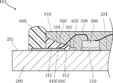
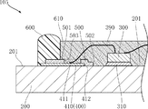
200 基板
201 主面
300 LEDチップ
301 サブマウント基板
310 接合層
320 LEDモジュール
321 実装端子
322 リフレクタ
323 蛍光樹脂
390 ワイヤ
400 配線パターン
410 パッド部
411 上面
412 端面
420 端子部
500 保護層
501 表面
502 端縁
503 開口
600 堰部
610 封止樹脂
620 ガラス層
621 ガラス層
710 グローブ
720 支持部材
730 放熱部材
740 電源部
750 ケーブル
760 口金
810 リフレクタ
820 筐体
830 コネクタ
840 ホルダ
Claims (37)
- 主面を有する基板と、
上記基板の上記主面に支持された複数のLEDチップと、
上記基板の上記主面上に形成され、上記複数のLEDチップと導通する配線パターンと、
上記基板の上記主面上に設けられており、上記複数のLEDチップを囲む枠状の堰部と、
を備えたLED照明器具であって、
上記配線パターンは、上記堰部と上記複数のLEDチップとの間に位置する部分を有する1以上のパッド部を有しており、
平面視において上記堰部に囲まれているとともに上記パッド部の少なくとも一部を覆い且つ上記LEDチップと離間して設けられた保護層を備え、
上記保護層は、上記堰部側から上記堰部と反対側の端部に向かう傾斜を備えており、
上記傾斜は、上記保護層において、上記堰部に接する端部から上記堰部と反対側の端部まで一様に続いていることを特徴とする、LED照明器具。 - 上記保護層は、上記堰部の内部に接している、請求項1に記載のLED照明器具。
- 上記パッド部のうち上記堰部によって囲まれた部分において上記基板の上記主面と同じ方向を向く面は、上記保護層に覆われている、請求項1または2に記載のLED照明器具。
- 上記パッド部のうち上記複数のLEDチップに臨む端面は、上記保護層に覆われている、請求項1ないし3のいずれかに記載のLED照明器具。
- 上記パッド部は、上記基板と上記堰部との間に介在する部分を有する、請求項1ないし4のいずれかに記載のLED照明器具。
- 上記配線パターンは、上記堰部の外側に位置する端子部を有する、請求項1ないし5のいずれかに記載のLED照明器具。
- 上記配線パターンは、上記複数のLEDチップを挟んで、2つの上記パッド部を有する、請求項1ないし6のいずれかに記載のLED照明器具。
- 上記配線パターンは、上記堰部に囲まれた領域において、上記2つのパッド部のみを有する、請求項7に記載のLED照明器具。
- 上記保護層は、上記複数のLEDチップを挟んで上記2つのパッド部を各別に覆う2つの部分を有する、請求項7または8に記載のLED照明器具。
- 上記保護層は、樹脂材料およびこの樹脂材料に混入された白色材料からなる、請求項1ないし9のいずれかに記載のLED照明器具。
- 上記樹脂材料はシリコーン樹脂である、請求項10に記載のLED照明器具。
- 上記白色材料は、酸化チタンである、請求項10または11に記載のLED照明器具。
- 上記保護層は、ガラスからなる、請求項1ないし9のいずれかに記載のLED照明器具。
- 上記堰部と上記複数のLEDチップとの間に位置するガラス層を有しており、
上記保護層のうち上記複数のLEDチップに臨む端縁は、上記ガラス層と重なっている、請求項1ないし13のいずれかに記載のLED照明器具。 - 上記LEDチップは、上記主面に直接接合されたベアチップである、請求項1ないし14のいずれかに記載のLED照明器具。
- 隣合う上記LEDチップどうしがワイヤによって接続されている、請求項14に記載のLED照明器具。
- 上記複数のLEDチップのいずれかと上記パッド部とがワイヤによって接続されている、請求項16に記載のLED照明器具。
- 上記堰部に囲まれた空間において上記複数のLEDチップおよび上記保護層を覆う封止樹脂を備える、請求項15ないし17のいずれかに記載のLED照明器具。
- 上記封止樹脂には、上記LEDチップからの光によって励起されることにより上記LEDチップからの光とは異なる波長の光を発する蛍光材料が混入されている、請求項18に記載のLED照明器具。
- 各々が、上記LEDチップ、このLEDチップを覆う蛍光樹脂、および実装端子を有する複数のLEDモジュールを備える、請求項1ないし14のいずれかに記載のLED照明器具。
- 上記基板は、セラミックスからなる、請求項1ないし20のいずれかに記載のLED照明器具。
- 上記基板は、アルミからなる、請求項1ないし20のいずれかに記載のLED照明器具。
- 上記配線パターンは、Agを含む、請求項1ないし22のいずれかに記載のLED照明器具。
- 上記保護層は、堰部に沿って全周に形成されている、請求項1ないし23のいずれかに記載のLED照明器具。
- 上記複数のLEDチップからの光を透過させるグローブをさらに備えることにより、LED電球として構成されている、請求項1ないし24のいずれかに記載のLED照明器具。
- 上記複数のLEDチップを囲むテーパ状のリフレクタをさらに備えることにより、ダウンライトとして構成されている、請求項1ないし24のいずれかに記載のLED照明器具。
- 上記パッド部は、上記複数のLEDチップを挟んで第1のパッド部と第2のパッド部との少なくとも2つが備えられ、
上記第1のパッド部と上記第2のパッド部とは、互いに直列に電気的に接続された上記複数のLEDチップを介して接続されている、請求項1ないし26のいずれかに記載のLED照明器具。 - 上記保護層は、上記基板の上記主面上において、上記パッド部の少なくとも一部を覆い、且つ上記堰部側から上記堰部と反対側の端部に向かって上記基板の主面からの全ての部分の高さが一様に減少するように形成されている、請求項1ないし27のいずれかに記載のLED照明器具。
- 主面を有する基板と、
上記基板の上記主面上に配置されたLEDチップと、
上記基板の上記主面上に設けられており、平面視において上記LEDチップを囲む堰部と、
上記堰部の外部から上記堰部の内部まで延在して設けられた配線と、
上記堰部に囲まれ、上記堰部に密着し、上記LEDチップと離間し、且つ上記配線の少なくとも一部を覆う第1絶縁層と、を有し、
上記第1絶縁層は、上記基板と垂直方向の高さが上記堰部側から一様に減少する傾斜を備えていることを特徴とする、LEDユニット。 - 上記第1絶縁層は、上記配線のうち上記LEDチップに対向する端部を覆っている、請求項29に記載のLEDユニット。
- 上記LEDチップと上記配線とを接続するワイヤを備えており、
上記第1絶縁層は、上記ワイヤの少なくとも一部を覆っている、請求項29または30に記載のLEDユニット。 - 上記LEDチップは、上記基板に対し接合層を介して相対的に固定されており、
上記第1絶縁層は上記接合層と離間して形成されている、請求項29ないし31のいずれかに記載のLEDユニット。 - 上記LEDチップと上記第1絶縁層とを覆い且つ上記LEDチップから発せられる光を透過させる第2絶縁層を有している、請求項29ないし32のいずれかに記載のLEDユニット。
- 上記堰部は、平面視において上記LEDチップを囲む環状構造となっており、
上記第1絶縁層は、上記堰部の環状構造に沿って上記LEDチップを囲んで形成されている、請求項29ないし33のいずれかに記載のLEDユニット。 - 上記第1絶縁層は、樹脂材料およびこの樹脂材料に混入された白色材料からなる、請求項29ないし34のいずれかに記載のLEDユニット。
- 上記樹脂材料はシリコーン樹脂である、請求項35に記載のLEDユニット。
- 上記白色材料は、酸化チタンである、請求項35または36に記載のLEDユニット。
Priority Applications (5)
| Application Number | Priority Date | Filing Date | Title |
|---|---|---|---|
| JP2012211724A JP6147977B2 (ja) | 2012-09-26 | 2012-09-26 | Led照明器具およびledユニット |
| US14/037,614 US9222625B2 (en) | 2012-09-26 | 2013-09-26 | LED lighting apparatus |
| US14/946,012 US9863584B2 (en) | 2012-09-26 | 2015-11-19 | LED lighting apparatus |
| US15/854,153 US10655793B2 (en) | 2012-09-26 | 2017-12-26 | LED lighting apparatus |
| US16/849,472 US10976011B2 (en) | 2012-09-26 | 2020-04-15 | LED lighting apparatus |
Applications Claiming Priority (1)
| Application Number | Priority Date | Filing Date | Title |
|---|---|---|---|
| JP2012211724A JP6147977B2 (ja) | 2012-09-26 | 2012-09-26 | Led照明器具およびledユニット |
Publications (3)
| Publication Number | Publication Date |
|---|---|
| JP2014067846A JP2014067846A (ja) | 2014-04-17 |
| JP2014067846A5 JP2014067846A5 (ja) | 2015-10-01 |
| JP6147977B2 true JP6147977B2 (ja) | 2017-06-14 |
Family
ID=50338662
Family Applications (1)
| Application Number | Title | Priority Date | Filing Date |
|---|---|---|---|
| JP2012211724A Expired - Fee Related JP6147977B2 (ja) | 2012-09-26 | 2012-09-26 | Led照明器具およびledユニット |
Country Status (2)
| Country | Link |
|---|---|
| US (4) | US9222625B2 (ja) |
| JP (1) | JP6147977B2 (ja) |
Families Citing this family (31)
| Publication number | Priority date | Publication date | Assignee | Title |
|---|---|---|---|---|
| JP6147977B2 (ja) * | 2012-09-26 | 2017-06-14 | ローム株式会社 | Led照明器具およびledユニット |
| JP5963001B2 (ja) * | 2013-03-28 | 2016-08-03 | 東芝ライテック株式会社 | 照明装置 |
| KR102080778B1 (ko) * | 2013-09-11 | 2020-04-14 | 엘지이노텍 주식회사 | 발광 소자 패키지 |
| DE202014001946U1 (de) * | 2014-02-28 | 2014-03-17 | Osram Gmbh | Lampe |
| WO2015139995A1 (en) | 2014-03-21 | 2015-09-24 | Koninklijke Philips N.V. | Lighting device with an improved housing |
| TWI613391B (zh) * | 2014-04-01 | 2018-02-01 | 晶元光電股份有限公司 | 發光二極體組件及應用此發光二極體組件的發光二極體燈泡 |
| JP2016115710A (ja) * | 2014-12-11 | 2016-06-23 | シチズン電子株式会社 | Led照明装置 |
| JP6541963B2 (ja) * | 2014-12-18 | 2019-07-10 | シチズン電子株式会社 | 発光装置及びその製造方法 |
| TW201631808A (zh) * | 2015-02-25 | 2016-09-01 | 隆達電子股份有限公司 | 發光二極體晶片封裝體 |
| JP6646969B2 (ja) * | 2015-08-03 | 2020-02-14 | シチズン電子株式会社 | 発光装置 |
| JP2017038031A (ja) * | 2015-08-14 | 2017-02-16 | シチズン電子株式会社 | 発光装置及びその製造方法 |
| US9859480B2 (en) | 2015-08-20 | 2018-01-02 | Nichia Corporation | Light emitting device and method of manufacturing light emitting device |
| JP6633881B2 (ja) | 2015-09-30 | 2020-01-22 | ローム株式会社 | Led照明器具およびその製造方法 |
| US9966515B2 (en) | 2015-12-26 | 2018-05-08 | Nichia Corporation | Light emitting device and method of manufacturing the light emitting device |
| CN110612611B (zh) * | 2016-05-24 | 2022-10-11 | 西铁城电子株式会社 | Led照明装置及led照明装置的制造方法 |
| JP6555243B2 (ja) | 2016-12-16 | 2019-08-07 | 日亜化学工業株式会社 | 発光装置および発光装置の製造方法 |
| JP6555242B2 (ja) | 2016-12-16 | 2019-08-07 | 日亜化学工業株式会社 | 発光装置および発光装置の製造方法 |
| US10411169B2 (en) | 2017-02-03 | 2019-09-10 | Nichia Corporation | Light emitting device having leads in resin package |
| JP7089343B2 (ja) * | 2017-04-13 | 2022-06-22 | ローム株式会社 | 半導体発光装置 |
| JP2018206886A (ja) * | 2017-06-01 | 2018-12-27 | パナソニックIpマネジメント株式会社 | 発光装置、及び、照明装置 |
| CN109244211A (zh) * | 2017-07-10 | 2019-01-18 | 罗冠杰 | 冲压封装发光二极管装置及其制造方法 |
| JP2019071352A (ja) * | 2017-10-10 | 2019-05-09 | シチズン電子株式会社 | 照明装置とその製造方法 |
| US10615319B2 (en) | 2017-10-20 | 2020-04-07 | Nichia Corporation | Light emitting device |
| JP6760324B2 (ja) | 2018-03-27 | 2020-09-23 | 日亜化学工業株式会社 | 発光装置 |
| US20190393112A1 (en) * | 2018-06-25 | 2019-12-26 | Elizabeth Nofen | Encapsulant material containing fluorophores for in-situ visualization of stress in an organic package |
| US11378259B2 (en) | 2018-12-19 | 2022-07-05 | Nichia Corporation | Light-emitting module |
| JP7219401B2 (ja) * | 2018-12-19 | 2023-02-08 | 日亜化学工業株式会社 | 発光モジュール |
| CN109887906A (zh) * | 2019-02-22 | 2019-06-14 | 福建天电光电有限公司 | 一种高反射led封装支架 |
| TWI880522B (zh) * | 2022-01-11 | 2025-04-11 | 隆達電子股份有限公司 | 無機發光二極體顯示器 |
| US12237451B2 (en) | 2022-01-28 | 2025-02-25 | Creeled, Inc. | Arrangements of light-altering coatings in light-emitting diode packages |
| JP7553830B2 (ja) * | 2022-04-19 | 2024-09-19 | 日亜化学工業株式会社 | 発光装置 |
Family Cites Families (16)
| Publication number | Priority date | Publication date | Assignee | Title |
|---|---|---|---|---|
| US7821023B2 (en) * | 2005-01-10 | 2010-10-26 | Cree, Inc. | Solid state lighting component |
| JP4973011B2 (ja) * | 2006-05-31 | 2012-07-11 | 豊田合成株式会社 | Led装置 |
| JP2009295892A (ja) * | 2008-06-09 | 2009-12-17 | Nichia Corp | 発光装置 |
| US7919339B2 (en) * | 2008-09-08 | 2011-04-05 | Iledm Photoelectronics, Inc. | Packaging method for light emitting diode module that includes fabricating frame around substrate |
| JP2010199547A (ja) * | 2009-01-30 | 2010-09-09 | Nichia Corp | 発光装置及びその製造方法 |
| CN102334202B (zh) * | 2009-02-27 | 2014-12-31 | 东芝照明技术株式会社 | 发光模块及照明装置 |
| CN102369607A (zh) * | 2009-03-31 | 2012-03-07 | 东芝照明技术株式会社 | 发光装置及照明装置 |
| JP5327472B2 (ja) | 2009-09-25 | 2013-10-30 | 東芝ライテック株式会社 | 電球形ランプおよび照明器具 |
| US8324789B2 (en) * | 2009-09-25 | 2012-12-04 | Toshiba Lighting & Technology Corporation | Self-ballasted lamp and lighting equipment |
| JP5612991B2 (ja) * | 2010-09-30 | 2014-10-22 | シャープ株式会社 | 発光装置及びこれを備えた照明装置 |
| JP5886584B2 (ja) * | 2010-11-05 | 2016-03-16 | ローム株式会社 | 半導体発光装置 |
| JP2012109478A (ja) * | 2010-11-19 | 2012-06-07 | Toshiba Lighting & Technology Corp | 発光体および照明装置 |
| US9461023B2 (en) * | 2011-10-28 | 2016-10-04 | Bridgelux, Inc. | Jetting a highly reflective layer onto an LED assembly |
| JP5673190B2 (ja) * | 2011-02-18 | 2015-02-18 | 日亜化学工業株式会社 | 発光装置 |
| US8507047B2 (en) * | 2011-10-13 | 2013-08-13 | Intematix Corporation | Method and system for manufacturing photo-luminescent wavelength conversion component |
| JP6147977B2 (ja) * | 2012-09-26 | 2017-06-14 | ローム株式会社 | Led照明器具およびledユニット |
-
2012
- 2012-09-26 JP JP2012211724A patent/JP6147977B2/ja not_active Expired - Fee Related
-
2013
- 2013-09-26 US US14/037,614 patent/US9222625B2/en active Active
-
2015
- 2015-11-19 US US14/946,012 patent/US9863584B2/en not_active Expired - Fee Related
-
2017
- 2017-12-26 US US15/854,153 patent/US10655793B2/en active Active
-
2020
- 2020-04-15 US US16/849,472 patent/US10976011B2/en active Active
Also Published As
| Publication number | Publication date |
|---|---|
| US10655793B2 (en) | 2020-05-19 |
| US9863584B2 (en) | 2018-01-09 |
| US20140085884A1 (en) | 2014-03-27 |
| US10976011B2 (en) | 2021-04-13 |
| US20180119890A1 (en) | 2018-05-03 |
| US9222625B2 (en) | 2015-12-29 |
| JP2014067846A (ja) | 2014-04-17 |
| US20160069517A1 (en) | 2016-03-10 |
| US20200240591A1 (en) | 2020-07-30 |
Similar Documents
| Publication | Publication Date | Title |
|---|---|---|
| JP6147977B2 (ja) | Led照明器具およびledユニット | |
| JP5203528B2 (ja) | 発光モジュール、光源装置、液晶表示装置および発光モジュールの製造方法 | |
| US9488345B2 (en) | Light emitting device, illumination apparatus including the same, and mounting substrate | |
| CN103430339B (zh) | 基板、发光装置以及照明装置 | |
| US20120300430A1 (en) | Light-emitting module and lighting apparatus | |
| JP5291268B1 (ja) | 発光モジュールおよびこれを用いた照明用光源、照明装置 | |
| US9196584B2 (en) | Light-emitting device and lighting apparatus using the same | |
| US10337704B2 (en) | Illumination light source having fastener fastening a pedestal and cover together with a mounting substrate interposed therebetween and light emitting elements surround the cover, the entirety of which is spaced in a horizontal direction from the light emitting elements | |
| US20150214451A1 (en) | Light-emitting module | |
| JP5993497B2 (ja) | Led照明装置 | |
| US9443832B2 (en) | Light emitting device, light source for illumination, and illumination apparatus | |
| JP2018206886A (ja) | 発光装置、及び、照明装置 | |
| WO2012057276A1 (ja) | 発光モジュール、および照明器具 | |
| JP2012015329A (ja) | 回路板 | |
| JP2011134934A (ja) | 発光モジュールおよび照明装置 | |
| JP2015133455A (ja) | 発光装置、照明用光源、および照明装置 | |
| JP2015060972A (ja) | 発光モジュール、照明装置および照明器具 | |
| CN103367343A (zh) | 发光模块 | |
| JP2019016728A (ja) | 発光装置、照明装置、及び、実装基板 | |
| JP2013073983A (ja) | 発光装置及び照明装置 | |
| JP2015133450A (ja) | 発光装置、照明用光源、および照明装置 | |
| JP2014067678A (ja) | Led照明器具 | |
| JP2014011015A (ja) | 照明器具 | |
| WO2013046292A1 (ja) | 発光モジュール、および照明器具 | |
| JP2019021665A (ja) | 発光装置、照明装置、及び、実装基板 |
Legal Events
| Date | Code | Title | Description |
|---|---|---|---|
| A521 | Request for written amendment filed |
Free format text: JAPANESE INTERMEDIATE CODE: A523 Effective date: 20150818 |
|
| A621 | Written request for application examination |
Free format text: JAPANESE INTERMEDIATE CODE: A621 Effective date: 20150909 |
|
| A977 | Report on retrieval |
Free format text: JAPANESE INTERMEDIATE CODE: A971007 Effective date: 20160427 |
|
| A131 | Notification of reasons for refusal |
Free format text: JAPANESE INTERMEDIATE CODE: A131 Effective date: 20160510 |
|
| A521 | Request for written amendment filed |
Free format text: JAPANESE INTERMEDIATE CODE: A523 Effective date: 20160708 |
|
| A131 | Notification of reasons for refusal |
Free format text: JAPANESE INTERMEDIATE CODE: A131 Effective date: 20161115 |
|
| A521 | Request for written amendment filed |
Free format text: JAPANESE INTERMEDIATE CODE: A523 Effective date: 20170112 |
|
| TRDD | Decision of grant or rejection written | ||
| A01 | Written decision to grant a patent or to grant a registration (utility model) |
Free format text: JAPANESE INTERMEDIATE CODE: A01 Effective date: 20170509 |
|
| A61 | First payment of annual fees (during grant procedure) |
Free format text: JAPANESE INTERMEDIATE CODE: A61 Effective date: 20170518 |
|
| R150 | Certificate of patent or registration of utility model |
Ref document number: 6147977 Country of ref document: JP Free format text: JAPANESE INTERMEDIATE CODE: R150 |
|
| R250 | Receipt of annual fees |
Free format text: JAPANESE INTERMEDIATE CODE: R250 |
|
| R250 | Receipt of annual fees |
Free format text: JAPANESE INTERMEDIATE CODE: R250 |
|
| R250 | Receipt of annual fees |
Free format text: JAPANESE INTERMEDIATE CODE: R250 |
|
| R250 | Receipt of annual fees |
Free format text: JAPANESE INTERMEDIATE CODE: R250 |
|
| R250 | Receipt of annual fees |
Free format text: JAPANESE INTERMEDIATE CODE: R250 |
|
| LAPS | Cancellation because of no payment of annual fees |