JP6168904B2 - 導波管平面線路変換器 - Google Patents
導波管平面線路変換器 Download PDFInfo
- Publication number
- JP6168904B2 JP6168904B2 JP2013163658A JP2013163658A JP6168904B2 JP 6168904 B2 JP6168904 B2 JP 6168904B2 JP 2013163658 A JP2013163658 A JP 2013163658A JP 2013163658 A JP2013163658 A JP 2013163658A JP 6168904 B2 JP6168904 B2 JP 6168904B2
- Authority
- JP
- Japan
- Prior art keywords
- waveguide
- dielectric substrate
- line converter
- short
- tapered
- Prior art date
- Legal status (The legal status is an assumption and is not a legal conclusion. Google has not performed a legal analysis and makes no representation as to the accuracy of the status listed.)
- Active
Links
- 239000000758 substrate Substances 0.000 claims description 57
- 230000005284 excitation Effects 0.000 description 37
- 230000005540 biological transmission Effects 0.000 description 32
- 238000003780 insertion Methods 0.000 description 11
- 230000037431 insertion Effects 0.000 description 11
- 239000004020 conductor Substances 0.000 description 5
- 229910052751 metal Inorganic materials 0.000 description 4
- 239000002184 metal Substances 0.000 description 4
- 230000001902 propagating effect Effects 0.000 description 4
- 238000010586 diagram Methods 0.000 description 3
- 238000005530 etching Methods 0.000 description 3
- 238000004519 manufacturing process Methods 0.000 description 3
- 238000000059 patterning Methods 0.000 description 3
- 238000004088 simulation Methods 0.000 description 3
- 229910052782 aluminium Inorganic materials 0.000 description 2
- XAGFODPZIPBFFR-UHFFFAOYSA-N aluminium Chemical compound [Al] XAGFODPZIPBFFR-UHFFFAOYSA-N 0.000 description 2
- 230000003247 decreasing effect Effects 0.000 description 2
- -1 for example Inorganic materials 0.000 description 2
- 239000010409 thin film Substances 0.000 description 2
- RYGMFSIKBFXOCR-UHFFFAOYSA-N Copper Chemical compound [Cu] RYGMFSIKBFXOCR-UHFFFAOYSA-N 0.000 description 1
- 239000011889 copper foil Substances 0.000 description 1
- 230000007423 decrease Effects 0.000 description 1
- 239000003822 epoxy resin Substances 0.000 description 1
- 238000002474 experimental method Methods 0.000 description 1
- 239000000463 material Substances 0.000 description 1
- 238000000034 method Methods 0.000 description 1
- 229920000647 polyepoxide Polymers 0.000 description 1
- 229920005989 resin Polymers 0.000 description 1
- 239000011347 resin Substances 0.000 description 1
Images


Landscapes
- Waveguide Connection Structure (AREA)
Description
<導波管平面線路変換器1>
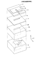
図1は、本発明の実施の形態1による導波管平面線路変換器1の一構成例を分解して示した斜視図である。図中には、矩形導波管2に連結される導波管平面線路変換器1が矩形導波管2の管軸方向を鉛直方向と一致させて描画されている。ここでは、水平面内で矩形導波管2の広壁Ww及び狭壁Wnと直交する方向をそれぞれx方向及びy方向と呼び、鉛直方向をz方向と呼ぶことにする。
実施の形態1では、導波管平面線路変換器1が導波路10aの両広壁Ww1を傾斜させたテーパー導波管10を備える場合の例について説明した。これに対し、本実施の形態では、導波路10aの一方の広壁Ww1だけを傾斜させたテーパー導波管10を備える場合について説明する。
10 テーパー導波管
10a 導波路
10b 先端開口
11 接地板
11a 励振スロット
12 誘電体基板
13 MSL
14 短絡板
14a 切り込み
14b,14c 外縁
2 矩形導波管
Rc 閉鎖領域
Wn 矩形導波管2の狭壁
Ww 矩形導波管2の広壁
Wn1 テーパー導波管10の狭壁
Ww1 テーパー導波管10の広壁
Claims (3)
- 矩形導波管に連通する導波路を有し、上記導波路が中空部からなり、上記導波路の広壁を傾斜させて先端開口を上記矩形導波管の断面よりも狭くしたテーパー導波管と、
一方の主面が上記テーパー導波管を閉鎖し、他方の主面上にマイクロストリップ線路及び短絡板が形成された誘電体基板とを備え、
上記短絡板は、領域全体が上記先端開口と重複している上記誘電体基板上の閉鎖領域を覆うとともに、上記マイクロストリップ線路を配置するための切り込みが形成された連続領域からなり、
上記マイクロストリップ線路は、上記閉鎖領域の長辺を跨いでいることを特徴とする導波管平面線路変換器。 - 上記テーパー導波管及び上記誘電体基板間に配置され、孔全体が上記先端開口と重複している細長い矩形形状の貫通孔を有する接地板を備えたことを特徴とする請求項1に記載の導波管平面線路変換器。
- 上記短絡板は、上記閉鎖領域の長辺と略平行であって、上記閉鎖領域の上記長辺から管内波長の略1/4倍だけ外側に形成された外縁を有し、
上記マイクロストリップ線路は、管内波長の0.4倍以上かつ0.6倍以下の距離だけ上記外縁から内側に挿入されていることを特徴とする請求項1又は2に記載の導波管平面線路変換器。
Priority Applications (1)
| Application Number | Priority Date | Filing Date | Title |
|---|---|---|---|
| JP2013163658A JP6168904B2 (ja) | 2013-08-06 | 2013-08-06 | 導波管平面線路変換器 |
Applications Claiming Priority (1)
| Application Number | Priority Date | Filing Date | Title |
|---|---|---|---|
| JP2013163658A JP6168904B2 (ja) | 2013-08-06 | 2013-08-06 | 導波管平面線路変換器 |
Publications (2)
| Publication Number | Publication Date |
|---|---|
| JP2015033099A JP2015033099A (ja) | 2015-02-16 |
| JP6168904B2 true JP6168904B2 (ja) | 2017-07-26 |
Family
ID=52518053
Family Applications (1)
| Application Number | Title | Priority Date | Filing Date |
|---|---|---|---|
| JP2013163658A Active JP6168904B2 (ja) | 2013-08-06 | 2013-08-06 | 導波管平面線路変換器 |
Country Status (1)
| Country | Link |
|---|---|
| JP (1) | JP6168904B2 (ja) |
Families Citing this family (1)
| Publication number | Priority date | Publication date | Assignee | Title |
|---|---|---|---|---|
| JP6415790B2 (ja) | 2016-07-05 | 2018-10-31 | 三菱電機株式会社 | 導波管−平面導波路変換器 |
Family Cites Families (2)
| Publication number | Priority date | Publication date | Assignee | Title |
|---|---|---|---|---|
| JP4375310B2 (ja) * | 2005-09-07 | 2009-12-02 | 株式会社デンソー | 導波管・ストリップ線路変換器 |
| JP5566169B2 (ja) * | 2010-04-07 | 2014-08-06 | 日本ピラー工業株式会社 | アンテナ装置 |
-
2013
- 2013-08-06 JP JP2013163658A patent/JP6168904B2/ja active Active
Also Published As
| Publication number | Publication date |
|---|---|
| JP2015033099A (ja) | 2015-02-16 |
Similar Documents
| Publication | Publication Date | Title |
|---|---|---|
| CN103187631B (zh) | 波导管缝隙天线 | |
| JP5566169B2 (ja) | アンテナ装置 | |
| KR101405068B1 (ko) | 고주파 신호 선로 | |
| JP5788548B2 (ja) | マイクロストリップアンテナ | |
| KR20210088527A (ko) | 고주파 필터 및 그러한 고주파 필터를 포함하는 위상 배열 안테나 | |
| JP6470930B2 (ja) | 分配器及び平面アンテナ | |
| TW202141851A (zh) | 天線結構及具有該天線結構之電子設備 | |
| KR102224626B1 (ko) | 도파관 슬롯 어레이 안테나 | |
| JP5586755B1 (ja) | アンテナ | |
| JP4753981B2 (ja) | 導波管・ストリップ線路変換器 | |
| JP7220540B2 (ja) | ホーンアンテナ | |
| US20090224858A1 (en) | High frequency device equipped with plurality of rectangular waveguide | |
| WO2020071316A1 (ja) | 平面アンテナ及び窓ガラス | |
| JP6168904B2 (ja) | 導波管平面線路変換器 | |
| JP6184802B2 (ja) | スロットアンテナ | |
| JP4794616B2 (ja) | 導波管・ストリップ線路変換器 | |
| JP5429459B2 (ja) | ミリ波アンテナ | |
| JP2004266380A (ja) | Nrdガイドモードサプレサ | |
| WO2016111107A1 (ja) | ホーンアンテナ | |
| JPWO2009048095A1 (ja) | 伝送線路を有する回路装置及びプリント回路基板 | |
| CN120357170B (zh) | 端射天线及设备 | |
| JP6497328B2 (ja) | 導波管終端器 | |
| JP4795225B2 (ja) | 誘電体導波管スロットアンテナ | |
| JP2006081160A (ja) | 伝送路変換器 | |
| CN111384590A (zh) | 激励器以及印刷电路板通信系统 |
Legal Events
| Date | Code | Title | Description |
|---|---|---|---|
| A621 | Written request for application examination |
Free format text: JAPANESE INTERMEDIATE CODE: A621 Effective date: 20160308 |
|
| A131 | Notification of reasons for refusal |
Free format text: JAPANESE INTERMEDIATE CODE: A131 Effective date: 20170217 |
|
| A521 | Request for written amendment filed |
Free format text: JAPANESE INTERMEDIATE CODE: A523 Effective date: 20170414 |
|
| TRDD | Decision of grant or rejection written | ||
| A01 | Written decision to grant a patent or to grant a registration (utility model) |
Free format text: JAPANESE INTERMEDIATE CODE: A01 Effective date: 20170627 |
|
| A61 | First payment of annual fees (during grant procedure) |
Free format text: JAPANESE INTERMEDIATE CODE: A61 Effective date: 20170627 |
|
| R150 | Certificate of patent or registration of utility model |
Ref document number: 6168904 Country of ref document: JP Free format text: JAPANESE INTERMEDIATE CODE: R150 |
|
| S533 | Written request for registration of change of name |
Free format text: JAPANESE INTERMEDIATE CODE: R313533 |
|
| R350 | Written notification of registration of transfer |
Free format text: JAPANESE INTERMEDIATE CODE: R350 |