JP6180318B2 - Comparator circuit - Google Patents
Comparator circuit Download PDFInfo
- Publication number
- JP6180318B2 JP6180318B2 JP2013270704A JP2013270704A JP6180318B2 JP 6180318 B2 JP6180318 B2 JP 6180318B2 JP 2013270704 A JP2013270704 A JP 2013270704A JP 2013270704 A JP2013270704 A JP 2013270704A JP 6180318 B2 JP6180318 B2 JP 6180318B2
- Authority
- JP
- Japan
- Prior art keywords
- current
- circuit
- unit
- control
- signal
- Prior art date
- Legal status (The legal status is an assumption and is not a legal conclusion. Google has not performed a legal analysis and makes no representation as to the accuracy of the status listed.)
- Expired - Fee Related
Links
Images






Classifications
-
- H—ELECTRICITY
- H03—ELECTRONIC CIRCUITRY
- H03K—PULSE TECHNIQUE
- H03K5/00—Manipulating of pulses not covered by one of the other main groups of this subclass
- H03K5/22—Circuits having more than one input and one output for comparing pulses or pulse trains with each other according to input signal characteristics, e.g. slope, integral
- H03K5/24—Circuits having more than one input and one output for comparing pulses or pulse trains with each other according to input signal characteristics, e.g. slope, integral the characteristic being amplitude
- H03K5/2472—Circuits having more than one input and one output for comparing pulses or pulse trains with each other according to input signal characteristics, e.g. slope, integral the characteristic being amplitude using field effect transistors
- H03K5/2481—Circuits having more than one input and one output for comparing pulses or pulse trains with each other according to input signal characteristics, e.g. slope, integral the characteristic being amplitude using field effect transistors with at least one differential stage
-
- G—PHYSICS
- G09—EDUCATION; CRYPTOGRAPHY; DISPLAY; ADVERTISING; SEALS
- G09G—ARRANGEMENTS OR CIRCUITS FOR CONTROL OF INDICATING DEVICES USING STATIC MEANS TO PRESENT VARIABLE INFORMATION
- G09G3/00—Control arrangements or circuits, of interest only in connection with visual indicators other than cathode-ray tubes
- G09G3/20—Control arrangements or circuits, of interest only in connection with visual indicators other than cathode-ray tubes for presentation of an assembly of a number of characters, e.g. a page, by composing the assembly by combination of individual elements arranged in a matrix no fixed position being assigned to or needed to be assigned to the individual characters or partial characters
- G09G3/2007—Display of intermediate tones
- G09G3/2014—Display of intermediate tones by modulation of the duration of a single pulse during which the logic level remains constant
-
- G—PHYSICS
- G09—EDUCATION; CRYPTOGRAPHY; DISPLAY; ADVERTISING; SEALS
- G09G—ARRANGEMENTS OR CIRCUITS FOR CONTROL OF INDICATING DEVICES USING STATIC MEANS TO PRESENT VARIABLE INFORMATION
- G09G3/00—Control arrangements or circuits, of interest only in connection with visual indicators other than cathode-ray tubes
- G09G3/20—Control arrangements or circuits, of interest only in connection with visual indicators other than cathode-ray tubes for presentation of an assembly of a number of characters, e.g. a page, by composing the assembly by combination of individual elements arranged in a matrix no fixed position being assigned to or needed to be assigned to the individual characters or partial characters
- G09G3/22—Control arrangements or circuits, of interest only in connection with visual indicators other than cathode-ray tubes for presentation of an assembly of a number of characters, e.g. a page, by composing the assembly by combination of individual elements arranged in a matrix no fixed position being assigned to or needed to be assigned to the individual characters or partial characters using controlled light sources
- G09G3/30—Control arrangements or circuits, of interest only in connection with visual indicators other than cathode-ray tubes for presentation of an assembly of a number of characters, e.g. a page, by composing the assembly by combination of individual elements arranged in a matrix no fixed position being assigned to or needed to be assigned to the individual characters or partial characters using controlled light sources using electroluminescent panels
- G09G3/32—Control arrangements or circuits, of interest only in connection with visual indicators other than cathode-ray tubes for presentation of an assembly of a number of characters, e.g. a page, by composing the assembly by combination of individual elements arranged in a matrix no fixed position being assigned to or needed to be assigned to the individual characters or partial characters using controlled light sources using electroluminescent panels semiconductive, e.g. using light-emitting diodes [LED]
-
- G—PHYSICS
- G09—EDUCATION; CRYPTOGRAPHY; DISPLAY; ADVERTISING; SEALS
- G09G—ARRANGEMENTS OR CIRCUITS FOR CONTROL OF INDICATING DEVICES USING STATIC MEANS TO PRESENT VARIABLE INFORMATION
- G09G3/00—Control arrangements or circuits, of interest only in connection with visual indicators other than cathode-ray tubes
- G09G3/20—Control arrangements or circuits, of interest only in connection with visual indicators other than cathode-ray tubes for presentation of an assembly of a number of characters, e.g. a page, by composing the assembly by combination of individual elements arranged in a matrix no fixed position being assigned to or needed to be assigned to the individual characters or partial characters
- G09G3/22—Control arrangements or circuits, of interest only in connection with visual indicators other than cathode-ray tubes for presentation of an assembly of a number of characters, e.g. a page, by composing the assembly by combination of individual elements arranged in a matrix no fixed position being assigned to or needed to be assigned to the individual characters or partial characters using controlled light sources
- G09G3/30—Control arrangements or circuits, of interest only in connection with visual indicators other than cathode-ray tubes for presentation of an assembly of a number of characters, e.g. a page, by composing the assembly by combination of individual elements arranged in a matrix no fixed position being assigned to or needed to be assigned to the individual characters or partial characters using controlled light sources using electroluminescent panels
- G09G3/32—Control arrangements or circuits, of interest only in connection with visual indicators other than cathode-ray tubes for presentation of an assembly of a number of characters, e.g. a page, by composing the assembly by combination of individual elements arranged in a matrix no fixed position being assigned to or needed to be assigned to the individual characters or partial characters using controlled light sources using electroluminescent panels semiconductive, e.g. using light-emitting diodes [LED]
- G09G3/3208—Control arrangements or circuits, of interest only in connection with visual indicators other than cathode-ray tubes for presentation of an assembly of a number of characters, e.g. a page, by composing the assembly by combination of individual elements arranged in a matrix no fixed position being assigned to or needed to be assigned to the individual characters or partial characters using controlled light sources using electroluminescent panels semiconductive, e.g. using light-emitting diodes [LED] organic, e.g. using organic light-emitting diodes [OLED]
- G09G3/3225—Control arrangements or circuits, of interest only in connection with visual indicators other than cathode-ray tubes for presentation of an assembly of a number of characters, e.g. a page, by composing the assembly by combination of individual elements arranged in a matrix no fixed position being assigned to or needed to be assigned to the individual characters or partial characters using controlled light sources using electroluminescent panels semiconductive, e.g. using light-emitting diodes [LED] organic, e.g. using organic light-emitting diodes [OLED] using an active matrix
- G09G3/3233—Control arrangements or circuits, of interest only in connection with visual indicators other than cathode-ray tubes for presentation of an assembly of a number of characters, e.g. a page, by composing the assembly by combination of individual elements arranged in a matrix no fixed position being assigned to or needed to be assigned to the individual characters or partial characters using controlled light sources using electroluminescent panels semiconductive, e.g. using light-emitting diodes [LED] organic, e.g. using organic light-emitting diodes [OLED] using an active matrix with pixel circuitry controlling the current through the light-emitting element
-
- H—ELECTRICITY
- H04—ELECTRIC COMMUNICATION TECHNIQUE
- H04N—PICTORIAL COMMUNICATION, e.g. TELEVISION
- H04N25/00—Circuitry of solid-state image sensors [SSIS]; Control thereof
-
- H—ELECTRICITY
- H04—ELECTRIC COMMUNICATION TECHNIQUE
- H04N—PICTORIAL COMMUNICATION, e.g. TELEVISION
- H04N25/00—Circuitry of solid-state image sensors [SSIS]; Control thereof
- H04N25/70—SSIS architectures; Circuits associated therewith
- H04N25/76—Addressed sensors, e.g. MOS or CMOS sensors
- H04N25/7795—Circuitry for generating timing or clock signals
-
- H—ELECTRICITY
- H04—ELECTRIC COMMUNICATION TECHNIQUE
- H04N—PICTORIAL COMMUNICATION, e.g. TELEVISION
- H04N25/00—Circuitry of solid-state image sensors [SSIS]; Control thereof
- H04N25/70—SSIS architectures; Circuits associated therewith
- H04N25/76—Addressed sensors, e.g. MOS or CMOS sensors
- H04N25/78—Readout circuits for addressed sensors, e.g. output amplifiers or A/D converters
-
- G—PHYSICS
- G09—EDUCATION; CRYPTOGRAPHY; DISPLAY; ADVERTISING; SEALS
- G09G—ARRANGEMENTS OR CIRCUITS FOR CONTROL OF INDICATING DEVICES USING STATIC MEANS TO PRESENT VARIABLE INFORMATION
- G09G2310/00—Command of the display device
- G09G2310/02—Addressing, scanning or driving the display screen or processing steps related thereto
- G09G2310/0264—Details of driving circuits
- G09G2310/0297—Special arrangements with multiplexing or demultiplexing of display data in the drivers for data electrodes, in a pre-processing circuitry delivering display data to said drivers or in the matrix panel, e.g. multiplexing plural data signals to one D/A converter or demultiplexing the D/A converter output to multiple columns
-
- G—PHYSICS
- G09—EDUCATION; CRYPTOGRAPHY; DISPLAY; ADVERTISING; SEALS
- G09G—ARRANGEMENTS OR CIRCUITS FOR CONTROL OF INDICATING DEVICES USING STATIC MEANS TO PRESENT VARIABLE INFORMATION
- G09G2310/00—Command of the display device
- G09G2310/06—Details of flat display driving waveforms
- G09G2310/066—Waveforms comprising a gently increasing or decreasing portion, e.g. ramp
-
- G—PHYSICS
- G09—EDUCATION; CRYPTOGRAPHY; DISPLAY; ADVERTISING; SEALS
- G09G—ARRANGEMENTS OR CIRCUITS FOR CONTROL OF INDICATING DEVICES USING STATIC MEANS TO PRESENT VARIABLE INFORMATION
- G09G2370/00—Aspects of data communication
- G09G2370/08—Details of image data interface between the display device controller and the data line driver circuit
Landscapes
- Engineering & Computer Science (AREA)
- Physics & Mathematics (AREA)
- Computer Hardware Design (AREA)
- General Physics & Mathematics (AREA)
- Theoretical Computer Science (AREA)
- Multimedia (AREA)
- Signal Processing (AREA)
- Nonlinear Science (AREA)
- Control Of Indicators Other Than Cathode Ray Tubes (AREA)
- Control Of El Displays (AREA)
- Analogue/Digital Conversion (AREA)
- Manipulation Of Pulses (AREA)
- Measurement Of Current Or Voltage (AREA)
Description
本開示は、コンパレータ回路、コンパレータ回路の制御方法、A/D変換回路、及び、表示装置に関する。 The present disclosure relates to a comparator circuit, a control method for the comparator circuit, an A / D conversion circuit, and a display device.
A/D変換回路などに用いられるコンパレータ回路として、2つの入力信号の差分を検出する差動回路部を用いた差動型のコンパレータ回路が知られている。この種のコンパレータ回路では、待機モードでの消費電力の低減を図るとともに、待機モードから通常動作モードへ移行する際の時間の短縮を図るために、差動回路部に供給する電流を待機モードと通常動作モードとで切り替えるようにしている(例えば、特許文献1参照)。 As a comparator circuit used in an A / D conversion circuit or the like, a differential comparator circuit using a differential circuit unit that detects a difference between two input signals is known. In this type of comparator circuit, in order to reduce the power consumption in the standby mode and to shorten the time when shifting from the standby mode to the normal operation mode, the current supplied to the differential circuit section is changed to the standby mode. Switching between the normal operation mode is performed (for example, see Patent Document 1).
上記の従来例に係るコンパレータ回路にあっては、待機モードと通常の比較動作モードとで、差動回路部に供給する電流を切り替えるに当たって、外部の制御部から与えられる制御信号に応じて切り替え制御を行う構成が採られている。しかしながら、外部からの指令(制御信号)に基づく切り替え制御では、制御部に対してあらかじめ設定されたシーケンス通りにしか電流の切り替え制御を行うことができない。そのため、例えば、差動回路部の動作状態に合わせた、消費電力の最適化を図るのが難しかった。 In the comparator circuit according to the conventional example described above, switching control is performed according to a control signal supplied from an external control unit when switching the current supplied to the differential circuit unit between the standby mode and the normal comparison operation mode. The structure which performs is taken. However, in the switching control based on an external command (control signal), the current switching control can be performed only in a sequence preset for the control unit. Therefore, for example, it has been difficult to optimize power consumption in accordance with the operation state of the differential circuit section.
そこで、本開示は、差動回路部の動作状態に合わせた、消費電力の最適化を図ることにより、消費電力の更なる低減が可能なコンパレータ回路、コンパレータ回路の制御方法、並びに、当該コンパレータ回路を有するA/D変換回路及び表示装置を提供することを目的とする。 Therefore, the present disclosure provides a comparator circuit capable of further reducing power consumption by optimizing power consumption in accordance with the operation state of the differential circuit unit, a method for controlling the comparator circuit, and the comparator circuit. It is an object to provide an A / D conversion circuit and a display device having the following.
上記の目的を達成するための本開示のコンパレータ回路は、
2つの入力信号の差分を検出する差動回路部と、
差動回路部に電流を供給する電流供給部と、
差動回路部の動作タイミングを検出し、その検出結果に応じて電流供給部が差動回路部に対して供給する電流を制御する制御部と、
を備える。
In order to achieve the above object, a comparator circuit of the present disclosure includes:
A differential circuit section for detecting a difference between two input signals;
A current supply unit for supplying current to the differential circuit unit;
A control unit that detects an operation timing of the differential circuit unit and controls a current supplied to the differential circuit unit by the current supply unit according to the detection result;
Is provided.
上記の目的を達成するための本開示のコンパレータ回路の制御方法は、
2つの入力信号の差分を検出する差動回路部と、
差動回路部に電流を供給する電流供給部と、
を備えるコンパレータ回路の制御に当たって、
差動回路部の動作タイミングを検出し、その検出結果に応じて電流供給部が差動回路部に対して供給する電流を制御する。
In order to achieve the above object, a method for controlling a comparator circuit of the present disclosure includes:
A differential circuit section for detecting a difference between two input signals;
A current supply unit for supplying current to the differential circuit unit;
In controlling a comparator circuit comprising
The operation timing of the differential circuit unit is detected, and the current supplied to the differential circuit unit by the current supply unit is controlled according to the detection result.
上記の目的を達成するための本開示のA/D変換回路は、
2つの入力信号の差分を検出する差動回路部と、
差動回路部に電流を供給する電流供給部と、
差動回路部の動作タイミングを検出し、その検出結果に応じて電流供給部が差動回路部に対して供給する電流を制御する制御部と、
を備えるコンパレータ回路を有する。
In order to achieve the above object, an A / D conversion circuit of the present disclosure includes:
A differential circuit section for detecting a difference between two input signals;
A current supply unit for supplying current to the differential circuit unit;
A control unit that detects an operation timing of the differential circuit unit and controls a current supplied to the differential circuit unit by the current supply unit according to the detection result;
A comparator circuit.
上記の目的を達成するための本開示の表示装置は、
発光部、及び、発光部を駆動する駆動回路から構成された複数の画素が2次元マトリクス状に配置されて成り、
駆動回路は、
信号電圧と制御波形とを比較するコンパレータ回路、及び、
コンパレータ回路の出力に応じて発光部を駆動する駆動用トランジスタ、
を有しており、
コンパレータ回路は、
信号電圧と制御波形との差分を検出する差動回路部と、
差動回路部に電流を供給する電流供給部と、
差動回路部の動作タイミングを検出し、その検出結果に応じて電流供給部が差動回路部に対して供給する電流を制御する制御部と、
を備える。
In order to achieve the above object, a display device of the present disclosure is provided.
A plurality of pixels composed of a light emitting unit and a driving circuit that drives the light emitting unit are arranged in a two-dimensional matrix,
The drive circuit
A comparator circuit for comparing the signal voltage with the control waveform; and
A driving transistor for driving the light emitting unit according to the output of the comparator circuit;
Have
The comparator circuit
A differential circuit section for detecting a difference between the signal voltage and the control waveform;
A current supply unit for supplying current to the differential circuit unit;
A control unit that detects an operation timing of the differential circuit unit and controls a current supplied to the differential circuit unit by the current supply unit according to the detection result;
Is provided.
上記の構成において、差動回路部の動作タイミングを検出し、その検出結果に応じて電流供給部が差動回路部に供給する電流を制御する制御部を有する(内蔵する)ことで、コンパレータ回路自身で差動回路部の動作状態を把握して電流制御を行うことができる。すなわち、コンパレータ回路は、外部から制御信号を受けて電流制御を行うのではなく、差動回路部の動作状態に応じて電流制御を行うことができる。これにより、差動回路部の動作状態に合わせた、消費電力の最適化を図ることができる。 In the above configuration, the comparator circuit has a built-in control unit that detects the operation timing of the differential circuit unit and controls the current supplied from the current supply unit to the differential circuit unit according to the detection result. The current state can be controlled by grasping the operating state of the differential circuit section by itself. That is, the comparator circuit can perform current control according to the operation state of the differential circuit unit, instead of performing current control by receiving a control signal from the outside. Thereby, power consumption can be optimized in accordance with the operation state of the differential circuit section.
本開示によれば、差動回路部の動作状態に合わせた、消費電力の最適化を図ることができるため、あらかじめ設定されたシーケンス通りに電流制御を行う場合よりも消費電力の低減が可能となる。
尚、ここに記載された効果に必ずしも限定されるものではなく、本明細書中に記載されたいずれかの効果であってもよい。また、本明細書に記載された効果はあくまで例示であって、これに限定されるものではなく、また付加的な効果があってもよい。
According to the present disclosure, the power consumption can be optimized in accordance with the operation state of the differential circuit unit, so that the power consumption can be reduced as compared with the case where the current control is performed according to a preset sequence. Become.
The effects described here are not necessarily limited, and any of the effects described in the present specification may be used. Moreover, the effect described in this specification is an illustration to the last, Comprising: It is not limited to this, There may be an additional effect.
以下、本開示の技術を実施するための形態(以下、「実施形態」と記述する)について図面を用いて詳細に説明する。本開示の技術は実施形態に限定されるものではなく、実施形態における種々の数値などは例示である。以下の説明において、同一要素又は同一機能を有する要素には同一符号を用いることとし、重複する説明は省略する。尚、説明は以下の順序で行う。
1.本開示のコンパレータ回路、コンパレータ回路の制御方法、A/D変換回路、及び、表示装置、全般に関する説明
2.実施例1(コンパレータ回路の例1)
3.実施例2(コンパレータ回路の例2)
4.実施例3(コンパレータ回路の例3)
5.実施例4(コンパレータ回路の例4)
6.実施例5(コンパレータ回路の例5)
7.実施例6(表示装置の例)
8.実施例7(列並列A/D変換方式の固体撮像装置の例)
Hereinafter, modes for carrying out the technology of the present disclosure (hereinafter referred to as “embodiments”) will be described in detail with reference to the drawings. The technology of the present disclosure is not limited to the embodiments, and various numerical values in the embodiments are examples. In the following description, the same reference numerals are used for the same elements or elements having the same function, and redundant description is omitted. The description will be given in the following order.
1. 1. General Description of Comparator Circuit, Comparator Circuit Control Method, A / D Conversion Circuit, and Display Device of the Present Disclosure Example 1 (Example 1 of a comparator circuit)
3. Example 2 (Example 2 of a comparator circuit)
4). Example 3 (Example 3 of comparator circuit)
5. Example 4 (Example 4 of a comparator circuit)
6). Example 5 (Example 5 of comparator circuit)
7). Example 6 (Example of display device)
8). Example 7 (Example of solid-state imaging device of column parallel A / D conversion method)
<本開示のコンパレータ回路、コンパレータ回路の制御方法、A/D変換回路、及び、表示装置、全般に関する説明>
本開示の技術が適用されるコンパレータ回路としては、どのような型式のコンパレータ回路であってもよい。一例として、2つの入力信号の差分を検出する差動回路部を有するチョッパ型のコンパレータ回路や差動型のコンパレータ回路を例示することができる。
<General Description of Comparator Circuit, Comparator Circuit Control Method, A / D Conversion Circuit, and Display Device of Present Disclosure>
The comparator circuit to which the technology of the present disclosure is applied may be any type of comparator circuit. As an example, a chopper type comparator circuit or a differential type comparator circuit having a differential circuit unit for detecting a difference between two input signals can be exemplified.
本開示の技術が適用されるコンパレータ回路について、入力段にコンパレータ回路が設けられるA/D変換回路において、当該コンパレータ回路として用いる構成とすることができる。当該コンパレータ回路を用いるA/D変換回路は、例えば、列並列A/D変換方式の固体撮像装置におけるA/D変換回路として用いることができる。 A comparator circuit to which the technology of the present disclosure is applied can be configured to be used as the comparator circuit in an A / D conversion circuit in which a comparator circuit is provided in an input stage. An A / D conversion circuit using the comparator circuit can be used, for example, as an A / D conversion circuit in a column parallel A / D conversion type solid-state imaging device.
上述した好ましい構成を含む本開示のコンパレータ回路、A/D変換回路、及び、表示装置にあっては、電流供給部について、差動回路部に対して、第1の電流と、当該第1の電流よりも小さい第2の電流とを選択的に供給可能な構成とすることができる。また、制御部について、電流供給部に対して、差動回路部が待機状態にあるときに第2の電流を供給し、差動回路部が待機状態から動作状態に移行する直前に第2の電流の供給から第1の電流の供給に切り替える制御を行う構成とすることができる。 In the comparator circuit, the A / D conversion circuit, and the display device of the present disclosure including the preferable configuration described above, the first current and the first current with respect to the differential circuit unit with respect to the current supply unit The second current smaller than the current can be selectively supplied. Further, the control unit supplies a second current to the current supply unit when the differential circuit unit is in the standby state, and the second current immediately before the differential circuit unit shifts from the standby state to the operating state. It can be set as the structure which performs control which switches from supply of an electric current to supply of the 1st electric current.
また、上述した好ましい構成を含む本開示のコンパレータ回路、A/D変換回路、及び、表示装置にあっては、差動回路部について、2つの入力信号の差に応じた信号を出力する差動アンプ、及び、差動アンプの出力信号を入力とする第1のアンプを含む構成とすることができる。このとき、制御部について、差動アンプの出力信号を入力とする第2のアンプを含み、第2のアンプの出力信号に応じて電流供給部に対する第1の電流と第2の電流との切り替え制御を行う構成とすることができる。第2のアンプは、第1のアンプよりも小さい閾値電圧を有する。 In the comparator circuit, A / D conversion circuit, and display device of the present disclosure including the above-described preferred configuration, the differential circuit unit outputs a signal corresponding to the difference between two input signals. An amplifier and a first amplifier that receives the output signal of the differential amplifier can be included. At this time, the control unit includes a second amplifier that receives the output signal of the differential amplifier, and switches between the first current and the second current for the current supply unit according to the output signal of the second amplifier. It can be set as the structure which controls. The second amplifier has a smaller threshold voltage than the first amplifier.
あるいは又、上述した好ましい構成を含む本開示のコンパレータ回路、A/D変換回路、及び、表示装置にあっては、電流供給部について、第1の電流を供給する第1の電流源、電流制限部、及び、電流制限部の入出力端間を選択的に短絡するスイッチ回路を有する構成とすることができる。電流制限部は、第1の電流源から供給される第1の電流を制限して第2の電流とする。このとき、制御部について、スイッチ回路に対して、差動回路部が待機状態にあるときにオフ状態にし、差動回路部が待機状態から動作状態に移行する直前にオン状態にする制御を行う構成とすることができる。 Alternatively, in the comparator circuit, the A / D conversion circuit, and the display device of the present disclosure including the above-described preferable configuration, the current supply unit includes a first current source that supplies a first current and a current limit. And a switch circuit that selectively short-circuits between the input and output terminals of the current limiting unit. The current limiting unit limits the first current supplied from the first current source to a second current. At this time, the control unit controls the switch circuit to be turned off when the differential circuit unit is in a standby state, and to be turned on immediately before the differential circuit unit shifts from the standby state to the operating state. It can be configured.
また、上述した好ましい構成を含む本開示のコンパレータ回路、A/D変換回路、及び、表示装置にあっては、第1の電流源について、第1の電流に対応したチャネル長の第1の電流源トランジスタから成る構成とすることができる。このとき、電流制限部について、チャネル長が第1の電流源トランジスタよりも大きく、第1の電流源トランジスタに対して直列に接続されるとともに、スイッチ回路に対して並列に接続された第2の電流源トランジスタから成る構成とすることができる。 In the comparator circuit, A / D conversion circuit, and display device of the present disclosure including the above-described preferable configuration, the first current having a channel length corresponding to the first current is provided for the first current source. It can be configured by a source transistor. At this time, the current limiter has a channel length larger than that of the first current source transistor, is connected in series to the first current source transistor, and is connected in parallel to the switch circuit. It can be configured by a current source transistor.
あるいは又、上述した好ましい構成を含む本開示のコンパレータ回路、A/D変換回路、及び、表示装置にあっては、第1の電流源について、第1の電流に対応した第1のバイアス電圧がゲート電極に印加された第1の電流源トランジスタから成る構成とすることができる。このとき、電流制限部について、第1の電流源トランジスタから供給される第1の電流を第2の電流に絞る第2のバイアス電圧がゲート電極に印加され、第1の電流源トランジスタに対して直列に接続されるとともに、スイッチ回路に対して並列に接続された第3の電流源トランジスタから成る構成とすることができる。 Alternatively, in the comparator circuit, the A / D conversion circuit, and the display device according to the present disclosure including the above-described preferable configuration, the first bias voltage corresponding to the first current is applied to the first current source. It can be configured by a first current source transistor applied to the gate electrode. At this time, a second bias voltage for narrowing the first current supplied from the first current source transistor to the second current is applied to the gate electrode in the current limiting unit, and the first current source transistor A third current source transistor connected in series and connected in parallel to the switch circuit may be used.
あるいは又、上述した好ましい構成を含む本開示のコンパレータ回路、A/D変換回路、及び、表示装置にあっては、電流供給部について、第2の電流を供給する第2の電流源、及び、第2の電流と加算されて第1の電流となる第3の電流を供給する第3の電流源を有する構成とすることができる。このとき、制御部について、第3の電流源に対して、差動回路部が待機状態にあるときに非活性状態にし、差動回路部が待機状態から動作状態に移行する直前に活性状態にする制御を行う構成とすることができる。 Alternatively, in the comparator circuit, the A / D conversion circuit, and the display device of the present disclosure including the preferable configuration described above, a second current source that supplies a second current with respect to the current supply unit, and A configuration may be employed in which a third current source that supplies a third current that is added to the second current and becomes the first current is provided. At this time, the control unit is inactivated with respect to the third current source when the differential circuit unit is in the standby state, and is activated immediately before the differential circuit unit shifts from the standby state to the operating state. It can be set as the structure which performs this control.
また、上述した好ましい構成を含む本開示のコンパレータ回路、A/D変換回路、及び、表示装置にあっては、第2の電流源について、第2の電流に対応した第3のバイアス電圧がゲート電極に印加された第4の電流源トランジスタから成る構成とすることができる。このとき、第3の電流源について、第4の電流源トランジスタに対して並列に接続され、導通状態のときに第3の電流を出力する第5の電流源トランジスタから成る構成とすることができる。 In the comparator circuit, A / D conversion circuit, and display device of the present disclosure including the above-described preferable configuration, the third bias voltage corresponding to the second current is gated with respect to the second current source. It can be configured by a fourth current source transistor applied to the electrode. At this time, the third current source can be configured to include a fifth current source transistor that is connected in parallel to the fourth current source transistor and outputs the third current in the conductive state. .
また、上述した好ましい構成を含む本開示のコンパレータ回路、A/D変換回路、及び、表示装置にあっては、第2の電流源について、差動回路部が待機状態にある一定期間において、差動回路部への電流の供給を選択的に遮断する機能を有する構成とすることができる。また、差動回路部について、2つの入力信号の差に応じた信号を出力する差動アンプを有し、第2の電流源について、差動回路部が待機状態にある一定期間に、制御波形に応じてオフ状態となって差動アンプへの電流の供給を遮断する第1のスイッチ回路を有する構成とすることができる。また、第2の電流源について、オン/オフ動作することで、差動回路部の出力電圧を安定化する作用を為す第2のスイッチ回路を有する構成とすることができる。 Further, in the comparator circuit, the A / D conversion circuit, and the display device of the present disclosure including the preferable configuration described above, the difference between the second current source in a certain period in which the differential circuit unit is in a standby state. It can be set as the structure which has the function to interrupt | block selectively supply of the electric current to a dynamic circuit part. The differential circuit unit has a differential amplifier that outputs a signal corresponding to the difference between the two input signals, and the second current source has a control waveform during a certain period in which the differential circuit unit is in a standby state. Accordingly, the first switch circuit that is turned off in response to the current supply to the differential amplifier can be provided. Further, the second current source can be configured to have a second switch circuit that performs an operation of stabilizing the output voltage of the differential circuit section by performing an on / off operation.
あるいは又、上述した好ましい構成を含む本開示のコンパレータ回路、A/D変換回路、及び、表示装置にあっては、制御部について、第3のアンプを含み、第2のアンプの出力信号及び第3のアンプの出力信号に応じて電流供給部に対する第1の電流と第2の電流との切り替え制御を行う構成とすることができる。第3のアンプは、差動アンプの出力信号を入力とする、第1のアンプよりも大きい閾値電圧を有する。
Alternatively, in the comparator circuit, the A / D conversion circuit, and the display device of the present disclosure including the above-described preferable configuration, the control unit includes the third amplifier, and the output signal of the second amplifier and the second amplifier In accordance with the output signal of the
あるいは又、上述した好ましい構成を含む本開示のコンパレータ回路、A/D変換回路、及び、表示装置にあっては、2つの入力信号の一方が、映像信号の信号電圧であり、2つの入力信号の他方が、鋸波形の電圧変化を有する制御波形である構成とすることができる。 Alternatively, in the comparator circuit, the A / D conversion circuit, and the display device of the present disclosure including the preferable configuration described above, one of the two input signals is a signal voltage of the video signal, and the two input signals The other of them may be a control waveform having a sawtooth voltage change.
上述した好ましい構成を含む本開示の表示装置にあっては、複数の画素が第1の方向及び第2の方向に2次元マトリクス状に配列されている。この画素の配列において、第1の方向に沿って配列された画素群を『列方向画素群』と呼ぶ場合があるし、第2の方向に沿って配列された画素群を『行方向画素群』と呼ぶ場合がある。第1の方向を表示装置における垂直方向とし、第2の方向を表示装置における水平方向とした場合、列方向画素群とは垂直方向に配列された画素群を意味し、行方向画素群とは水平方向に配列された画素群を意味する。 In the display device of the present disclosure including the preferable configuration described above, a plurality of pixels are arranged in a two-dimensional matrix in the first direction and the second direction. In this pixel arrangement, a pixel group arranged along the first direction may be referred to as a “column direction pixel group”, and a pixel group arranged along the second direction may be referred to as a “row direction pixel group”. May be called. When the first direction is the vertical direction in the display device and the second direction is the horizontal direction in the display device, the column direction pixel group means a pixel group arranged in the vertical direction, and the row direction pixel group means It means a group of pixels arranged in the horizontal direction.
また、上述した好ましい構成を含む本開示の表示装置にあっては、複数の画素について、第1の方向及び第2の方向に2次元マトリクス状に配列され、画素群について第1の方向に沿ってP個の画素ブロックに分割された構成とすることができる。そして、第1番目の画素ブロックに属する画素を構成する発光部から、第P番目の画素ブロックに属する画素を構成する発光部まで、画素ブロック毎に、順次、一斉に発光させ、且つ、一部の画素ブロックに属する画素を構成する発光部を発光させているとき、残りの画素ブロックに属する画素を構成する発光部を発光させない形態とすることができる。 In the display device of the present disclosure including the above-described preferable configuration, the plurality of pixels are arranged in a two-dimensional matrix in the first direction and the second direction, and the pixel group is aligned in the first direction. Thus, the pixel block can be divided into P pixel blocks. Then, light is emitted from the light emitting units that constitute the pixels that belong to the first pixel block to the light emitting units that constitute the pixels that belong to the Pth pixel block, sequentially for each pixel block, and partly When the light emitting portions constituting the pixels belonging to the pixel block are caused to emit light, the light emitting portions constituting the pixels belonging to the remaining pixel blocks can be prevented from emitting light.
あるいは又、上述した好ましい構成を含む本開示の表示装置にあっては、複数の制御波形に基づき、発光部が、複数回、発光する構成とすることができる。そして、この場合、複数の制御波形の時間間隔は一定であることが好ましい。また、1表示フレーム内における制御波形の数よりも、1表示フレーム内における駆動回路に供給される制御波形の数は少ない形態とすることができる。この形態は、1表示フレームにおいて一連の複数の制御波形を生成し、一の画素ブロックに属する画素を構成する発光部を発光させないとき、一連の複数の制御波形の一部をマスクして、一の画素ブロックに属する画素を構成する駆動回路には制御波形を供給しないことで達成することができる。 Alternatively, in the display device of the present disclosure including the above-described preferable configuration, the light emitting unit can emit light a plurality of times based on a plurality of control waveforms. In this case, the time intervals of the plurality of control waveforms are preferably constant. In addition, the number of control waveforms supplied to the drive circuit in one display frame can be made smaller than the number of control waveforms in one display frame. This form generates a series of control waveforms in one display frame, and masks a part of the series of control waveforms when a light emitting unit constituting a pixel belonging to one pixel block does not emit light. This can be achieved by not supplying a control waveform to the drive circuits constituting the pixels belonging to the pixel block.
更には、以上に説明した各種の好ましい構成、形態を含む本開示の表示装置において、発光部は発光ダイオード(LED)から構成されている形態とすることができる。発光ダイオードは、周知の構成、構造の発光ダイオードとすることができる。即ち、発光ダイオードの発光色に依って、最適な構成、構造を有し、適切な材料から作製された発光ダイオードを選択すればよい。発光ダイオードを発光部とする表示装置にあっては、赤色発光ダイオードから成る発光部が赤色発光副画素(サブピクセル)として機能し、緑色発光ダイオードから成る発光部が緑色発光副画素として機能し、青色発光ダイオードから成る発光部が青色発光副画素として機能し、これらの3種類の副画素によって1画素が構成され、これらの3種類の副画素の発光状態によってカラー画像を表示することができる。 Furthermore, in the display device of the present disclosure including the various preferable configurations and forms described above, the light emitting unit may be configured by a light emitting diode (LED). The light emitting diode may be a light emitting diode having a known configuration and structure. That is, a light emitting diode having an optimal configuration and structure and made of an appropriate material may be selected depending on the light emitting color of the light emitting diode. In a display device having a light emitting diode as a light emitting unit, a light emitting unit composed of a red light emitting diode functions as a red light emitting subpixel, and a light emitting unit composed of a green light emitting diode functions as a green light emitting subpixel. A light emitting unit composed of a blue light emitting diode functions as a blue light emitting subpixel, and one pixel is constituted by these three types of subpixels, and a color image can be displayed according to the light emission state of these three types of subpixels.
尚、本開示における『1画素』は、このような表示装置における「1副画素」に相当するので、このような表示装置における「1副画素」を、『1画素』と読み替えればよい。3種類の副画素によって1画素を構成する場合、3種類の副画素の配列として、デルタ配列、ストライプ配列、ダイアゴナル配列、レクタングル配列を挙げることができる。そして、発光ダイオードを、PWM駆動法に基づき、しかも、定電流駆動することで、発光ダイオードのスペクトル波長にブルーシフトが生じることを防止することができる。また、3つのパネルを準備し、第1のパネルを赤色発光ダイオードから成る発光部から構成し、第2のパネルを緑色発光ダイオードから成る発光部から構成し、第3のパネルを青色発光ダイオードから成る発光部から構成し、これらの3つのパネルからの光を、例えば、ダイクロイック・プリズムを用いて纏めるプロジェクタへ適用することもできる。 Note that “1 pixel” in the present disclosure corresponds to “1 subpixel” in such a display device, and thus “1 subpixel” in such a display device may be read as “1 pixel”. When one pixel is constituted by three types of subpixels, examples of the arrangement of the three types of subpixels include a delta arrangement, a stripe arrangement, a diagonal arrangement, and a rectangle arrangement. Then, by driving the light emitting diode based on the PWM driving method and at a constant current, it is possible to prevent a blue shift from occurring in the spectral wavelength of the light emitting diode. In addition, three panels are prepared, the first panel is composed of a light emitting unit composed of a red light emitting diode, the second panel is composed of a light emitting unit composed of a green light emitting diode, and the third panel is composed of a blue light emitting diode. It is also possible to apply the light from these three panels to a projector that uses, for example, a dichroic prism.
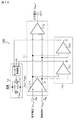
図1は、本開示の実施例1に係るコンパレータ回路の構成を示す回路図である。図1に示すように、実施例1に係るコンパレータ回路10Aは、2つの回路入力端子IN1,IN2及び1つの回路出力端子OUTに加えて、差動回路部11、電流供給部12、及び、制御部13を有する構成となっている。
FIG. 1 is a circuit diagram illustrating a configuration of a comparator circuit according to the first embodiment of the present disclosure. As shown in FIG. 1, a comparator circuit 10A according to the first embodiment includes a
差動回路部11は、2つの回路入力端子IN1,IN2に入力される2つの入力信号の差分を検出する。ここで、一方の回路入力端子IN1には、比較対象の信号である、例えば、映像信号の信号電圧VSigが入力される。他方の回路入力端子IN2には、比較基準の信号である、例えば、鋸波形の電圧変化を有する制御波形VSawが入力される。制御波形VSawは、コンパレータ回路の比較出力期間内において、例えば、最大レベルから所定の傾斜角度で下降し、最小レベルに達した後、同じ傾斜角度で上昇する鋸波形である。
The
電流供給部12は、差動回路部11に対して第1の電流と、当該第1の電流よりも小さい第2の電流とを選択的に供給可能な構成となっている。ここで、第1の電流は、差動回路部11を動作状態(アクティブ状態)にするための駆動電流(動作電流)IDrvである。また、第2の電流は、差動回路部11に対して待機状態(スタンバイ状態)のときに供給する待機電流(スタンバイ電流)IStbyである。待機電流IStbyは、差動回路部11が待機状態(待機モード)から動作状態(動作モード)に移行する際に、即ち、待機モードからの復帰の際に、セトリング不足が生じないようにできる程度の電流である。
The
制御部13は、差動回路部11の動作タイミングを検出する。ここで言う差動回路部11の動作タイミングとは、差動回路部11が待機状態(待機モード)から動作状態(動作モード)に移行するタイミング(即ち、動作状態に入るタイミング)や、差動回路部11が待機状態から動作状態に移行する直前のタイミングや、動作状態から待機状態に移行するタイミングなどである。
The
制御部13は、差動回路部11の動作タイミングを検出したら、その検出結果に応じて電流供給部12が差動回路部11に対して供給する電流を制御する。具体的には、制御部13は、電流供給部12に対して、差動回路部11が待機状態にあるときに第2の電流、即ち、待機電流IStbyを供給する制御を行う。制御部13は更に、電流供給部12に対して、差動回路部11が待機状態から動作状態に移行する直前のタイミングで、待機電流IStbyの供給から第1の電流、即ち、駆動電流IDrvの供給に切り替える制御を行う。
When detecting the operation timing of the
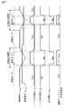
図2は、実施例1に係るコンパレータ回路10Aの回路動作の説明に供するタイミング波形図である。図2には、制御波形VSaw、信号電圧VSig、ノードAの電位VA、ノードBの電位VB、及び、差動回路部11の出力電圧VOutの各波形と、差動回路部11の消費電流の推移を示している。ここで、ノードAは差動回路部11の出力ノードであり、ノードBは制御部13の出力ノードである。後述する各実施例においても同様である。
FIG. 2 is a timing waveform diagram for explaining the circuit operation of the comparator circuit 10A according to the first embodiment. FIG. 2 shows each waveform of the control waveform V Saw , the signal voltage V Sig , the potential V A of the node A , the potential V B of the node B , and the output voltage V Out of the
差動回路部11は、制御波形VSawが信号電圧VSigを横切るタイミング(本例では、下回るタイミング)から、制御波形VSawが信号電圧VSigを再び横切るタイミング(本例では、上回るタイミング)までの期間が動作モードとなる。この動作モードで比較動作が実行され、低レベル(例えば、GNDレベル)の出力電圧VOutが回路出力端子OUTから出力される。
一方、差動回路部11の待機モードでは、電流供給部12から差動回路部11に対して待機電流IStby、即ち、差動回路部11が待機モードから動作モードに移行する際に、セトリング不足が生じないようにするための電流が供給された状態にある。待機電流IStbyは、駆動電流IDrvよりも小さい電流、より具体的には、セトリング不足が生じないようにできる程度に小さい電流である。従って、差動回路部11における待機モードでの消費電力を、動作モードでの消費電力よりも低く抑えることができる。また、動作モードに移行する前に、差動回路部11に待機電流IStbyが流れていることで、動作モードへの移行の際に、セトリング不足が生じることもない。
On the other hand, in the standby mode of the
差動回路部11の出力ノードであるノードAの電位VAは、制御波形VSawの鋸波形の電圧変化に対応して変化する。このノードAの電位VAを制御部13が監視する。そして、制御部13は、ノードAの電位VAが所定のレベルを超えるタイミングを検出する。この所定のレベルは、差動回路部11が待機状態から動作状態に移行する直前のタイミングを検出可能なレベル、本例では、GND(接地)+αのレベルに設定される。ここで、後述する実施例2のように、差動回路部11の出力段にアンプ(第1のアンプ112に相当)を配置する構成を採る場合は、当該アンプの閾値電圧をVth1とすると、αは、GND<GND+α<Vth1の条件を満足する値に設定される。
The potential V A of the node A that is the output node of the
ノードAの電位VAがGND+αのレベルを超えると、制御部13の出力ノードであるノードBの電位VBが電源電位VDDからGNDレベルに遷移する。このノードBの電位VBの遷移を受けて、電流供給部12は、差動回路部11に対して供給する電流を、待機電流IStbyから駆動電流IDrvに切り替える。これにより、セトリング不足を生じることなく、待機モードから動作モードへ移行できるとともに、当該動作モードにおいて駆動電流IDrvによる駆動の下に、比較動作を確実に行うことが可能になる。
When the potential V A of the node A exceeds the level of GND + α, the potential V B of the node B that is the output node of the
上述したように、実施例1に係るコンパレータ回路10Aにあっては、外部からの指令(制御信号)に基づいて電流の制御を行うのではなく、内蔵する制御部13の制御の下に、コンパレータ回路自身で差動回路部11の動作状態を把握して電流の制御を行う構成を採っている。すなわち、コンパレータ回路10Aは、外部から制御信号を受けて電流制御を行うのではなく、差動回路部11の動作状態に応じて電流制御を行う。
As described above, in the comparator circuit 10A according to the first embodiment, the current is not controlled based on an external command (control signal), but the comparator is controlled under the control of the built-in
これにより、差動回路部11の動作状態に合わせた、消費電力の最適化を図ることができるため、あらかじめ設定されたシーケンス通りに電流制御を行う場合よりも、コンパレータ回路の消費電力の低減が可能となる。また、差動回路部11の動作状態に応じて電流制御を行う制御部13を内蔵していることで、外部から制御信号を受けて電流制御を行う場合のような、制御信号を伝送するための配線が不要になる利点もある。
As a result, the power consumption can be optimized in accordance with the operation state of the
この配線が不要になる利点については、特に、コンパレータ回路を複数設け、これら複数のコンパレータ回路を異なるタイミングで動作させるようなシステム構成を採る場合に有効に作用する。具体的には、外部の制御部から制御信号を受けて電流制御を行う場合には、複数のコンパレータ回路毎に制御部、及び、外部から制御信号を伝送する配線が必要になるが、制御部13を内蔵する構成となっていることでその必要がないため、システム全体として、ロジック回路やアナログ回路への配線数を削減できる。 The advantage of eliminating the need for wiring is particularly effective when a system configuration is employed in which a plurality of comparator circuits are provided and the plurality of comparator circuits are operated at different timings. Specifically, when current control is performed by receiving a control signal from an external control unit, a control unit and wiring for transmitting the control signal from the outside are required for each of the plurality of comparator circuits. 13 is built-in, and this is not necessary. Therefore, the number of wires to the logic circuit and analog circuit can be reduced as a whole system.
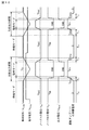
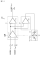
図3は、本開示の実施例2に係るコンパレータ回路の構成を示す回路図である。また、図4は、実施例2に係るコンパレータ回路の回路動作の説明に供するタイミング波形図であり、制御波形VSaw、信号電圧VSig、ノードAの電位VA、ノードBの電位VB、及び、出力電圧VOutの各波形と、差動アンプ111の消費電流の推移を示している。
FIG. 3 is a circuit diagram illustrating a configuration of the comparator circuit according to the second embodiment of the present disclosure. FIG. 4 is a timing waveform diagram for explaining the circuit operation of the comparator circuit according to the second embodiment. The control waveform V Saw , the signal voltage V Sig , the potential V A of the node A , the potential V B of the node B , In addition, each waveform of the output voltage V Out and the transition of current consumption of the
実施例2に係るコンパレータ回路10Bは、差動回路部11、電流供給部12、及び、制御部13を有し、一方の回路入力端子IN1に映像信号の信号電圧VSigが入力され、他方の回路入力端子IN2に制御波形VSawが入力される点で、実施例1に係るコンパレータ回路10Aと同じである。
The
実施例2に係るコンパレータ回路10Bにおいて、差動回路部11は、2つの入力信号、即ち、信号電圧VSigと制御波形VSawとの差に応じた信号を出力する差動アンプ111と、差動アンプ111の出力信号を入力とするアンプ(第1のアンプ)112とから成る構成となっている。アンプ112は、差動アンプ111の出力信号が閾値電圧Vth1を超えると、低レベルの出力電圧VOutを、本コンパレータ回路10Bの比較結果として出力する。
In the
電流供給部12は、第1の電流源121、電流制限部122、及び、スイッチ回路123を有する構成となっている。第1の電流源121は、第1の電流である駆動電流IDrvを出力する。電流制限部122は、第1の電流源121から供給される駆動電流IDrvを第2の電流である待機電流IStbyに制限する(絞る)。スイッチ回路123は、電流制限部122の入出力端間を選択的に短絡する。
The
この電流供給部12において、スイッチ回路123がオン(閉)状態にあるときは、当該スイッチ回路123によって電流制限部122の入出力端間が短絡されるため、第1の電流源121から出力される駆動電流IDrvがそのまま差動アンプ111に供給される。また、スイッチ回路123がオフ(開)状態にあるときは、駆動電流IDrvが電流制限部122で電流制限される(電流が絞られる)ことによって得られる待機電流IStbyが差動アンプ111に供給される。
In the
制御部13は、差動アンプ111の出力信号を入力とするアンプ(第2のアンプ)131から構成されている。制御部13のアンプ131は、差動回路部11のアンプ112の閾値電圧Vth1よりも小さい閾値電圧Vth2(Vth1>Vth2)を有し、差動アンプ111の出力信号が閾値電圧Vth2を超えると、低レベル(例えば、GNDレベル)の信号を出力する。この出力信号は、電流供給部12に対して駆動電流IDrvと待機電流IStbyとの切り替え制御を行う電流切替え制御信号として供給される。
The
ここで、差動アンプ111の出力信号(ノードAの電位VA)が閾値電圧Vth2を超えるタイミングは、差動回路部11、即ち、差動アンプ111が待機状態から動作状態に移行する直前のタイミングである。従って、制御部13は、スイッチ回路123に対して、電流切替え制御信号による制御の下に、差動アンプ111が待機状態にあるときにオフ状態にし、差動アンプ111が待機状態から動作状態に移行する直前にオン状態にする切り替え制御を行うことになる。
Here, the timing at which the output signal of the differential amplifier 111 (the potential V A of the node A) exceeds the threshold voltage V th2 is immediately before the
図5に、実施例2に係るコンパレータ回路10Bにおける電流供給部12の具体的な回路構成例を示す。
FIG. 5 illustrates a specific circuit configuration example of the
(回路例1に係る電流供給部)
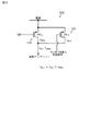
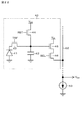
図5Aは、回路例1に係る電流供給部12Aの回路構成を示す回路図である。回路例1に係る電流供給部12Aにあっては、第1の電流源121は、第1の電流源トランジスタ、例えば、Pチャネル型電界効果トランジスタTR11から成る。このPチャネル型電界効果トランジスタTR11では、チャネル長L、チャネル幅W、ゲート電極に印加されるバイアス電圧VBなどに基づいて駆動電流IDrvが決定される。
(Current supply unit according to circuit example 1)
FIG. 5A is a circuit diagram illustrating a circuit configuration of a
電流制限部122は、チャネル長LがPチャネル型電界効果トランジスタTR11よりも大きく、当該電界効果トランジスタTR11に対して直列に接続された第2の電流源トランジスタ、例えば、Pチャネル型電界効果トランジスタTR12から成る。Pチャネル型電界効果トランジスタTR12のゲート電極には、Pチャネル型電界効果トランジスタTR11と同じバイアス電圧VBが印加されている。ここで、電界効果トランジスタにあっては、チャネル長とチャネル幅の比(W/L)が大きいほどの電流駆動能力が大きくなることが知られている。
The
従って、バイアス電圧VB及びチャネル幅Wを同じとした場合、Pチャネル型電界効果トランジスタTR12のチャネル長LをPチャネル型電界効果トランジスタTR11よりも大きくすることで、Pチャネル型電界効果トランジスタTR12の電流駆動能力がPチャネル型電界効果トランジスタTR11よりも小さくなる。これにより、第1の電流源121から出力される駆動電流IDrvを、電流制限部122において、待機電流IStbyに制限する(絞る)ことができる。
Therefore, when the same bias voltage VB and the channel width W, is made larger than the P-channel field effect transistor TR 11 the channel length L of the P-channel field effect transistor TR 12, P-channel field effect transistor TR The current drive capability of 12 is smaller than that of the P-channel field effect transistor TR 11 . Thus, the drive current I Drv output from the first
電流制限部122の入出力端間を選択的に短絡するスイッチ回路123は、Pチャネル型電界効果トランジスタTR12と並列に接続されたスイッチングトランジスタ、例えば、Pチャネル型電界効果トランジスタTR13から成る。このPチャネル型電界効果トランジスタTR13は、制御部13から低レベルの電流切替え制御信号がゲート電極に印加されたときにオン(導通)状態となってPチャネル型電界効果トランジスタTR12のソース−ドレイン間を短絡し、第1の電流源121から出力される駆動電流IDrvを差動アンプ111に供給する。
The
(回路例2に係る電流供給部)
図5Bは、回路例2に係る電流供給部12Bの回路構成を示す回路図である。回路例2に係る電流供給部12Bにあっても、回路例1に係る電流供給部12Aと同様に、第1の電流源121は、駆動電流IDrvに対応した第1のバイアス電圧VBがゲート電極に印加された第1の電流源トランジスタ、例えば、Pチャネル型電界効果トランジスタTR11から成る。
(Current supply unit according to circuit example 2)
FIG. 5B is a circuit diagram illustrating a circuit configuration of a
電流制限部122は、Pチャネル型電界効果トランジスタTR11から供給される駆動電流IDrvを待機電流IStbyに制限する(絞る)第2のバイアス電圧VB’がゲート電極に印加され、電界効果トランジスタTR11に対して直列に接続された第3の電流源トランジスタ、例えば、Pチャネル型電界効果トランジスタTR14から成る。スイッチ回路123についても、回路例1に係る電流供給部12Aと同様に、Pチャネル型電界効果トランジスタTR12と並列に接続されたスイッチングトランジスタ、例えば、Pチャネル型電界効果トランジスタTR13から成る。
The
上記の構成の実施例2に係るコンパレータ回路10Bにあっても、実施例1に係るコンパレータ回路10Aと同様の作用、効果を奏することができる。すなわち、外部から制御信号を受けて電流制御を行うのではなく、差動回路部11の動作状態に応じて電流制御を行うことができることで、差動回路部11の動作状態に合わせて消費電力を最適化することができるため、コンパレータ回路の消費電力の低減が可能となる。また、外部から制御信号を受けて電流制御を行う場合のような、制御信号を伝送するための配線が不要になる利点もある。
Even in the
図6は、本開示の実施例3に係るコンパレータ回路の構成を示す回路図である。また、図7は、実施例3に係るコンパレータ回路の回路動作の説明に供するタイミング波形図であり、制御波形VSaw、信号電圧VSig、ノードAの電位VA、ノードBの電位VB、及び、出力電圧VOutの各波形と、差動アンプ111の消費電流の推移を示している。
FIG. 6 is a circuit diagram illustrating a configuration of a comparator circuit according to the third embodiment of the present disclosure. FIG. 7 is a timing waveform diagram for explaining the circuit operation of the comparator circuit according to the third embodiment. The control waveform V Saw , the signal voltage V Sig , the potential V A of the node A , the potential V B of the node B , In addition, each waveform of the output voltage V Out and the transition of current consumption of the
実施例3に係るコンパレータ回路10Cは、差動回路部11、電流供給部12、及び、制御部13を有し、一方の回路入力端子IN1に映像信号の信号電圧VSigが入力され、他方の回路入力端子IN2に制御波形VSawが入力される点で、実施例1に係るコンパレータ回路10Aと同じである。また、差動回路部11及び制御部13の構成については、実施例2に係るコンパレータ回路10Bと同じである。
The
電流供給部12は、第2の電流源124と第3の電流源125との2つの電流源から成り、これらの電流源124,125が並列に接続された構成となっている。第2の電流源124は、第2の電流である待機電流IStbyを出力する。第3の電流源125は、待機電流IStbyと加算されて(加算されることによって)第1の電流、即ち、駆動電流IDrvとなる第3の電流IDrv’を出力する。
The
実施例3に係るコンパレータ回路10Cにあっては、制御部13の出力信号は、電流供給部12の第3の電流源125に対して、当該電流源125の活性状態(オン状態)/非活性状態(オフ状態)の切り替え制御を行うオン/オフ制御信号として供給される。具体的には、制御部13は、電流供給部12に供給するオン/オフ制御信号によって、差動アンプ111が待機状態から動作状態に移行する直前に第3の電流源125を活性状態にし, 差動アンプ111が待機状態にあるときに第3の電流源125を非活性状態にする制御を行う。
In the
電流供給部12において、第3の電流源125が非活性状態にあるときには、第2の電流源124から出力される待機電流IStbyがそのまま差動アンプ111に供給される。第3の電流源125が活性状態にあるときには、第2の電流源124から出力される待機電流IStbyと、第3の電流源125から出力される第3の電流IDrv’とが加算されて駆動電流IDrvとして差動アンプ111に供給される。
In the
(回路例3に係る電流供給部)
図8は、実施例3に係るコンパレータ回路における電流供給部(回路例3に係る電流供給部)の回路構成例を示す回路図である。回路例3に係る電流供給部12Cにおいて、第2の電流源124は、待機電流IStbyに対応した第3のバイアス電圧VB’がゲート電極に印加された第4の電流源トランジスタ、例えば、Pチャネル型電界効果トランジスタTR15から成る。第3の電流源125は、Pチャネル型電界効果トランジスタTR15に対して並列に接続され、導通(オン)状態のときに第3の電流IDrv’を出力する第5の電流源トランジスタ、例えば、Pチャネル型電界効果トランジスタTR16から成る。Pチャネル型電界効果トランジスタTR16のゲート電極には、制御部13から出力されるオン/オフ切替え制御信号が与えられる。
(Current supply unit according to circuit example 3)
FIG. 8 is a circuit diagram illustrating a circuit configuration example of a current supply unit (current supply unit according to circuit example 3) in the comparator circuit according to the third embodiment. In the
上記の構成の実施例3に係るコンパレータ回路10Cにあっても、実施例1に係るコンパレータ回路10Aと同様の作用、効果を奏することができる。すなわち、外部から制御信号を受けて電流制御を行うのではなく、差動回路部11の動作状態に応じて電流制御を行うことができることで、差動回路部11の動作状態に合わせて消費電力を最適化することができるため、コンパレータ回路の消費電力の低減が可能となる。また、外部から制御信号を受けて電流制御を行う場合のような、制御信号を伝送するための配線が不要になる利点もある。
Even in the
尚、回路例1乃至回路例3にあっては、第1の電流源121、電流制限部122、スイッチ回路123、第2の電流源124、及び、第3の電流源125を、Pチャネル型電界効果トランジスタで構成するとしたが、これに限られるものではない。すなわち、第1の電流源121、電流制限部122、スイッチ回路123、第2の電流源124、及び、第3の電流源125を、Nチャネル型電界効果トランジスタで構成することも可能であるし、Pチャネル型電界効果トランジスタとNチャネル型電界効果トランジスタとの組み合わせで構成することも可能である。
In the circuit example 1 to circuit example 3, the first
図9は、本開示の実施例4に係るコンパレータ回路の構成を示す回路図である。また、図10は、実施例4に係るコンパレータ回路の回路動作の説明に供するタイミング波形図であり、制御波形VSaw、信号電圧VSig、ノードAの電位VA、ノードBの電位VB、及び、出力電圧VOutの各波形と、差動アンプ111の消費電流の推移を示している。
FIG. 9 is a circuit diagram illustrating a configuration of a comparator circuit according to the fourth embodiment of the present disclosure. FIG. 10 is a timing waveform diagram for explaining the circuit operation of the comparator circuit according to the fourth embodiment. The control waveform V Saw , the signal voltage V Sig , the potential V A of the node A , the potential V B of the node B , In addition, each waveform of the output voltage V Out and the transition of current consumption of the
実施例4に係るコンパレータ回路10Dは、差動回路部11、電流供給部12、及び、制御部13を有し、一方の回路入力端子IN1に映像信号の信号電圧VSigが入力され、他方の回路入力端子IN2に制御波形VSawが入力される点で、実施例1に係るコンパレータ回路10Aと同じである。
A
また、差動回路部11及び制御部13の構成については、実施例3に係るコンパレータ回路10Cと同じである。電流供給部12は、待機電流IStbyを出力する第2の電流源124と、第3の電流IDrv’を出力する第3の電流源125との2つの電流源から成り、これらの電流源124,125が並列に接続された構成となっている。また、制御部13は、電流供給部12に供給するオン/オフ切替え制御信号によって、差動アンプ111が待機状態から動作状態に移行する直前に第3の電流源125を活性状態にし、差動アンプ111が待機状態にあるときに第3の電流源125を非活性状態にする制御を行う構成となっている。
The configurations of the
そして、実施例4に係るコンパレータ回路10Dにあっては、第2の電流源124は、差動回路部11、より具体的には、差動アンプ111が待機状態(待機モード)にある一定期間T0において、差動アンプ111への待機電流IStbyの供給を選択的に遮断する機能を有する。第2の電流源124における待機電流IStbyの選択的な遮断動作は、コンパレータ回路の比較出力期間内において、最大レベルと最小レベルとの間で所定の傾斜角度で下降/上昇を行う制御波形VSawに基づいて実行される。ここで、差動アンプ111が待機状態にある一定期間T0は、制御波形VSawが、最大レベルよりも所定レベルだけ低い設定レベルV0を基準とし、当該設定レベルV0よりも大きい期間となる。
In the
差動アンプ111が待機状態にある一定期間T0において、差動アンプ111への待機電流IStbyの供給が遮断されることで、当該一定期間T0における差動アンプ111の消費電流は0となる。そして、差動アンプ111に待機電流IStbyが供給される期間は、一定期間T0の終了後の僅かな期間T1と、一定期間T0の開始前の僅かな期間T2となる。期間T1は、一定期間T0の終了から差動アンプ111の出力信号(ノードAの電位VA)が閾値電圧Vth2を超えるまでの期間である。期間T2は、差動アンプ111の出力信号が閾値電圧Vth2以下になってから一定期間T0に入るまでの期間である。
When the supply of the standby current I Stby to the
(実施例4に係るコンパレータ回路の具体的な回路構成)
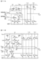
図11は、実施例4に係るコンパレータ回路10Dの具体的な回路構成を示す回路図であり、図11Aに回路例1に係る回路構成を示し、図11Bに回路例2に係る回路構成を示す。
(Specific circuit configuration of the comparator circuit according to the fourth embodiment)
11 is a circuit diagram illustrating a specific circuit configuration of the
(回路例1)
図11Aに示すように、差動アンプ111は、例えば、2つのPチャネル型電界効果トランジスタTR21,TR22と、2つのNチャネル型電界効果トランジスタTR23,TR24とから成る周知の差動アンプの構成となっている。2つのPチャネル型電界効果トランジスタTR21,TR22は、ソース電極が共通に接続されて差動動作を為す差動対トランジスタである。
(Circuit example 1)
As shown in FIG. 11A, the
2つのNチャネル型電界効果トランジスタTR23,TR24は、能動負荷となるカレントミラー回路を構成している。具体的には、Nチャネル型電界効果トランジスタTR23は、ドレイン電極及びゲート電極が共にPチャネル型電界効果トランジスタTR21のドレイン電極に接続され、ソース電極が低電位側の電源GNDに接続されている。Nチャネル型電界効果トランジスタTR24は、ゲート電極がNチャネル型電界効果トランジスタTR23のゲート電極に接続され、ドレイン電極がPチャネル型電界効果トランジスタTR22のドレイン電極に接続され、ソース電極が低電位側の電源GNDに接続されている。 The two N-channel field effect transistors TR 23 and TR 24 constitute a current mirror circuit serving as an active load. Specifically, the N-channel field effect transistor TR 23 has both a drain electrode and a gate electrode connected to the drain electrode of the P-channel field effect transistor TR 21 , and a source electrode connected to the power supply GND on the low potential side. Yes. The N-channel field effect transistor TR 24 has a gate electrode connected to the gate electrode of the N-channel field effect transistor TR 23 , a drain electrode connected to the drain electrode of the P-channel field effect transistor TR 22, and a low source electrode. It is connected to the power supply GND on the potential side.
上記の構成の差動アンプ111において、Pチャネル型電界効果トランジスタTR21のゲート電極が一方の入力端となり、映像信号の信号電圧VSigを入力とする。また、Pチャネル型電界効果トランジスタTR22のゲート電極が他方の入力端となり、鋸波形の電圧変化を有する制御波形VSawを入力とする。そして、Pチャネル型電界効果トランジスタTR22のドレイン電極とNチャネル型電界効果トランジスタTR24のドレイン電極との共通接続点(ノード)が差動アンプ111の出力端(ノードA)となる。
In the
第1のアンプ112は、電流源I1及びNチャネル型電界効果トランジスタTR25から成る構成となっている。電流源I1と電界効果トランジスタTR25とは、高電位側の電源VDDと低電位側の電源GNDとの間に直列に接続されている。電界効果トランジスタTR25のゲート電極は、差動アンプ111の出力端、即ち、ノードAに接続されている。そして、電流源I1と電界効果トランジスタTR25との共通接続点が、第1のアンプ112の出力端となり、本コンパレータ回路10Dの回路出力端子OUTに接続される。
The
制御部13を構成する第2のアンプ131は、電流源I2及びNチャネル型電界効果トランジスタTR26から成る構成となっている。電流源I2と電界効果トランジスタTR26とは、高電位側の電源VDDと低電位側の電源GNDとの間に直列に接続されている。電界効果トランジスタTR26のゲート電極は、差動アンプ111の出力端、即ち、ノードAに接続されている。そして、電流源I2と電界効果トランジスタTR26との共通接続点が、第2のアンプ131の出力端(ノードB)となる。このノードBに導出される信号は、電流供給部12に対して駆動電流IDrvと待機電流IStbyとの切り替え制御を行う電流切替え制御信号として供給される。
The
(回路例2)
回路例2では、主に、電流供給部12の具体的な回路構成について説明する。但し、差動アンプ111、第1のアンプ112、及び、第2のアンプ131の構成の一部が回路例1と若干異なっている。
(Circuit example 2)
In Circuit Example 2, a specific circuit configuration of the
差動アンプ111は、2つのPチャネル型電界効果トランジスタTR21,TR22、及び、2つのNチャネル型電界効果トランジスタTR23,TR24に加えて、Pチャネル型電界効果トランジスタTR27及びNチャネル型電界効果トランジスタTR28を有する構成となっている。これら電界効果トランジスタTR27,TR28は、高電位側の電源VDDと低電位側の電源GNDとの間に直列に接続されている。そして、電界効果トランジスタTR27は、ゲート電極とドレイン電極とが共通に接続されたダイオード接続構成となっている。また、電界効果トランジスタTR28は、電界効果トランジスタTR23とゲート電極が共通に接続されている。尚、電界効果トランジスタTR24は、ゲート電極とドレイン電極とが共通に接続されている。
In addition to the two P-channel field effect transistors TR 21 and TR 22 and the two N-channel field effect transistors TR 23 and TR 24 , the
電流供給部12は、電流源トランジスタとして、互いに直列に接続された例えば3つのPチャネル型電界効果トランジスタTR31,TR32,TR33を有する。これら電界効果トランジスタTR31,TR32,TR33の各ゲート電極には、駆動電流IDrvに対応したバイアス電圧VBが印加される。
The
ここで、電界効果トランジスタTR31は、駆動電流IDrvを生成する電流源トランジスタであり、Pチャネル型電界効果トランジスタTR36と共に第3の電流源125を構成している。そして、電界効果トランジスタTR36は、後述するスイッチ(第2のスイッチ回路)としての機能の他に、図3の電流制限部122と同様の機能を有し、駆動電流IDrvを第3の電流IDrv’に制限する(絞る)。2つの電界効果トランジスタTR32,TR33は、駆動電流IDrvを基に待機電流IStbyを生成する電流源トランジスタであり、第2の電流源124を構成している。すなわち、電界効果トランジスタTR32,TR33は、図3の電流制限部122と同様の機能を有し、駆動電流IDrvを待機電流IStbyに制限する(絞る)。
Here, the field effect transistor TR 31 is a current source transistor that generates the drive current I Drv , and constitutes a third
第2の電流源124は、電流源トランジスタであるPチャネル型電界効果トランジスタTR32,TR33に加えて、2つのスイッチ回路、即ち、第1のスイッチ回路21及び第2のスイッチ回路22を有する構成となっている。第1のスイッチ回路21は、Pチャネル型電界効果トランジスタTR34から成り、制御波形VSawに応じてオン/オフ動作する。第2のスイッチ回路22は、Pチャネル型電界効果トランジスタTR35から成り、差動回路部11の出力電圧VOutに応じてオン/オフ動作することで、後述するように、当該出力電圧VOutを安定化する作用を為す。
尚、図11Bの回路例では、第2のスイッチ回路22(電界効果トランジスタTR35)について、第1のスイッチ回路21(電界効果トランジスタTR34)に対して並列に配置した回路構成を採っているが、その配置位置はこれに限られるものではない。例えば、第2のスイッチ回路22を、電界効果トランジスタTR32のソース電極側に配置したり、電界効果トランジスタTR32と電界効果トランジスタTR33との間に配置したりする回路構成を採ることも可能である。更には、第2のスイッチ回路22を、第3の電流源125に対して並列に接続した回路構成を採ることも可能である。
The second
In the circuit example of FIG. 11B, the second switch circuit 22 (field effect transistor TR 35 ) is arranged in parallel with the first switch circuit 21 (field effect transistor TR 34 ). However, the arrangement position is not limited to this. For example, the
第3の電流源125は、電流源トランジスタであるPチャネル型電界効果トランジスタTR31に加えて、スイッチ回路23を有する構成となっている。スイッチ回路23は、先述した、駆動電流IDrvを第3の電流IDrv’に絞る機能を有するPチャネル型電界効果トランジスタTR36から成る。電界効果トランジスタTR36は、制御部13を構成する第2のアンプ131の出力信号(オン/オフ切替え制御信号)に応じてオン/オフ動作する。
The third
第1のアンプ112において、電流源I1は、Pチャネル型電界効果トランジスタTR29から構成されている。電界効果トランジスタTR29は、電界効果トランジスタTR25に対して直列に接続され、そのゲート電極が電界効果トランジスタTR27のゲート電極とドレイン電極との共通接続ノードに接続されている。第2のアンプ131において、電流源I2は、Pチャネル型電界効果トランジスタTR30から構成されている。電界効果トランジスタTR30は、電界効果トランジスタTR26に対して直列に接続され、そのゲート電極が電界効果トランジスタTR27のゲート電極とドレイン電極との共通接続ノードに接続されている。
In the
上記の構成の電流供給部12において、第2の電流源124の電界効果トランジスタTR34は、制御波形VSawに応じて(制御波形VSawの高レベル区間で)、差動アンプ111が待機状態にある一定期間T0にオフ状態となる。これにより、第2の電流源124から差動アンプ111への待機電流IStbyの供給が遮断(停止)される。ここで、一定期間T0を決める、先述した設定レベルV0(図10参照)は、Pチャネル型電界効果トランジスタTR34の閾値電圧に対応することになる。そして、差動アンプ111が待機状態にある一定期間T0において、差動アンプ111への待機電流IStbyの供給が遮断されることで、当該一定期間T0における差動アンプ111の消費電流は0となる。
In the
また、第2の電流源124の電界効果トランジスタTR35は、差動アンプ111、第1のアンプ112、及び、第2のアンプ131の出力値を電源電位VDDに固定するためのスイッチとして作用する。差動アンプ111への供給電流を0にすると、ノードA及びノードBの各電位、並びに、出力電圧VOutが不定値に成り易いが、電界効果トランジスタTR35から成る第2のスイッチ回路22の作用によってこれを解消することができる。具体的には、例えば出力電圧VOutが不定になり、電源電位VDDから下がってくると、電界効果トランジスタTR35オン状態になる。すると、コンパレータ回路10Dが動作状態になり、VSaw>VSigなら、出力電圧VOutが電源電位VDDになる。このようにして、電界効果トランジスタTR35は、出力電圧VOutが不定にならない状態にしている。出力電圧VOut等が不定にならないので、差動アンプ111への供給電流を0にすることができる。
The field effect transistor TR 35 of the second
また、第3の電流源125の電界効果トランジスタTR36は、第2のアンプ131から供給されるオン/オフ切替え制御信号に応じて、第3の電流源125の活性状態/非活性状態の切り替えを行う。具体的には、電界効果トランジスタTR36は、オン状態になることによって差動アンプ111への第3の電流IDrv’の供給を開始する(即ち、第3の電流源125を活性状態にする)。また、電界効果トランジスタTR36は、オフ状態になることによって差動アンプ111への第3の電流IDrv’の供給を停止する(即ち、第3の電流源125を非活性状態にする)。
The field effect transistor TR 36 of the third
上記の構成の実施例4に係るコンパレータ回路10Dにあっても、実施例1に係るコンパレータ回路10Aと同様の作用、効果を得ることができる。すなわち、外部から制御信号を受けて電流制御を行うのではなく、差動回路部11の動作状態に応じて電流制御を行うことができることで、差動回路部11の動作状態に合わせて消費電力を最適化することができるため、コンパレータ回路の消費電力の低減が可能となる。また、外部から制御信号を受けて電流制御を行う場合のような、制御信号を伝送するための配線が不要になる利点もある。
Even in the
実施例4に係るコンパレータ回路10Dにあっては更に、差動アンプ111が待機状態にある一定期間T0に、差動アンプ111への待機電流IStbyの供給を遮断し、消費電流を0にすることができるため、先の各実施例よりも差動回路部11の消費電力、ひいては、コンパレータ回路の消費電力を低減できる。
In the
図12は、本開示の実施例5に係るコンパレータ回路の構成を示す回路図である。また、図13は、実施例5に係るコンパレータ回路の回路動作の説明に供するタイミング波形図であり、制御波形VSaw、信号電圧VSig、ノードAの電位VA、ノードBの電位VB、ノードCの電位VC、及び、出力電圧VOutの各波形と、差動アンプ111の消費電流の推移を示している。
FIG. 12 is a circuit diagram illustrating a configuration of a comparator circuit according to the fifth embodiment of the present disclosure. FIG. 13 is a timing waveform diagram for explaining the circuit operation of the comparator circuit according to the fifth embodiment. The control waveform V Saw , the signal voltage V Sig , the potential V A of the node A , the potential V B of the node B , Each waveform of the potential V C of the node C and the output voltage V Out and the transition of the consumption current of the
実施例5に係るコンパレータ回路10Eは、差動回路部11、電流供給部12、及び、制御部13を有し、一方の回路入力端子IN1に映像信号の信号電圧VSigが入力され、他方の回路入力端子IN2に制御波形VSawが入力される点で、実施例1に係るコンパレータ回路10Aと同じである。また、差動回路部11の構成については、実施例2に係るコンパレータ回路10Bと同じである。
The
電流供給部12は、第2の電流である待機電流IStbyを出力する第2の電流源124、及び、第3の電流IDrv’を出力する第3の電流源125に加えて、第3の電流源125のオン/オフ制御を行うオン/オフ制御部126を有する構成となっている。オン/オフ制御部126は、制御部13から与えられる制御信号に基づいて、第3の電流源125のオン(活性)/オフ(非活性)の制御を行う。
In addition to the second
制御部13は、差動アンプ111の出力信号を入力とする2つのアンプ(第2のアンプ及び第3のアンプ)131,132から構成されている。アンプ131が差動回路部11のアンプ(第1のアンプ)112の閾値電圧Vth1よりも小さい閾値電圧Vth2(Vth1>Vth2)を有するのに対して、アンプ132は閾値電圧Vth1よりも大きい閾値電圧Vth3(Vth1<Vth3)を有している。
The
第2のアンプ131は、差動アンプ111のノードAの電位VAが閾値電圧Vth2を超えることで、低レベル(例えば、GNDレベル)の制御信号を出力する。第3のアンプ132は、差動アンプ111のノードAの電位VAが閾値電圧Vth2を超えることで、低レベル(例えば、GNDレベル)の制御信号を出力する。第2のアンプ131及び第3のアンプ132の各制御信号は、電流供給部12に対して第3の電流源125のオン/オフの制御を行うオン/オフ制御信号として供給される。
The
ここで、第2のアンプ131から低レベルの制御信号が出力される期間は、差動アンプ111が待機状態から動作状態に移行する直前のタイミングから、差動アンプ111が動作状態から待機状態に移行した直後のタイミングまでの期間である。また、第3のアンプ132から低レベルの制御信号が出力される期間は、制御波形VSawが信号電圧VSigを超えた(本例では、下回った)直後のタイミングから、制御波形VSawが再び信号電圧VSigを超える(本例では、上回る)直前のタイミングまでの期間である。
Here, during the period in which the low-level control signal is output from the
これら第2のアンプ131及び第3のアンプ132の各制御信号を受けて、電流供給部12のオン/オフ制御部126は、第3の電流源125を以下のようにオン/オフ制御する。先ず、差動アンプ111が待機状態にあるときに第3の電流源125をオフ状態にする。これにより、差動アンプ111が待機状態にあるときには当該差動アンプ111に対して、第2の電流源124から出力される待機電流IStbyがそのまま供給される。
In response to the control signals of the
次に、差動アンプ111が待機状態から動作状態に移行する直前のタイミングで、第2のアンプ131から出力される制御信号に応答して、第3の電流源125をオン状態にする。これにより、第2の電流源124から出力される待機電流IStbyと、第3の電流源125から出力される第3の電流IDrv’とが加算されて駆動電流IDrvとして差動アンプ111に供給される。
Next, the third
次に、制御波形VSawが信号電圧VSigを超えた(本例では、制御波形VSawが信号電圧VSigを下回った)直後のタイミングで、第3のアンプ132から出力される制御信号に応答して第3の電流源125をオフ状態にする。これにより、制御波形VSawが信号電圧VSigを超えた直後から差動アンプ111に対して、第2の電流源124から出力される待機電流IStbyが供給される。
Next, the control waveform V Saw exceeds a signal voltage V Sig (in the present embodiment, the control waveform V Saw is below the signal voltage V Sig) at timing immediately after, the control signal output from the
次いで、制御波形VSawが再び信号電圧VSigを超える(本例では、制御波形VSawが信号電圧VSigを上回る)直前のタイミングで、第3の電流源125をオン状態にする。これにより、第2の電流源124から出力される待機電流IStbyと、第3の電流源125から出力される第3の電流IDrv’とが加算されて駆動電流IDrvとして差動アンプ111に供給される。
Then, the control waveform V Saw again exceeds the signal voltage V Sig (in the present embodiment, the control waveform V Saw exceeds the signal voltage V Sig) at timing immediately before, the third
次に、差動アンプ111が動作状態から待機状態に移行した直後のタイミングで、第2のアンプ131から出力される制御信号に応答して、第3の電流源125をオフ状態にする。差動アンプ111が動作状態から待機状態に移行した直後から差動アンプ111に対して、第2の電流源124から出力される待機電流IStbyが供給される。
Next, in response to the control signal output from the
上述したように、第2のアンプ131及び第3のアンプ132の各制御信号に基づく、オン/オフ制御部126による制御の下に、差動アンプ111に対してその比較動作の前後の僅かな期間でのみ、駆動電流IDrvが供給され、それ以外の期間では待機電流IStbyが供給される制御が行われる。
As described above, the
ここで、差動アンプ111の比較動作とは、制御波形VSawが信号電圧VSigを超えることを検出する動作、及び、制御波形VSawが再び信号電圧VSigを超えることを検出する動作である。また、比較動作の前後の僅かな期間とは、待機状態から動作状態に移行する直前から制御波形VSawが信号電圧VSigを超えた直後までの期間、及び、制御波形VSawが再び信号電圧VSigを超える直前から動作状態から待機状態に移行した直後までの期間である。
Here, the comparison operation of the
上記の構成の実施例5に係るコンパレータ回路10Eにあっても、実施例1に係るコンパレータ回路10Aと同様の作用、効果を奏することができる。すなわち、外部から制御信号を受けて電流制御を行うのではなく、差動回路部11の動作状態に応じて電流制御を行うことができることで、差動回路部11の動作状態に合わせて消費電力を最適化することができるため、コンパレータ回路の消費電力の低減が可能となる。また、外部から制御信号を受けて電流制御を行う場合のような、制御信号を伝送するための配線が不要になる利点もある。
Even in the
実施例5に係るコンパレータ回路10Eにあっては更に、差動アンプ111に対して比較動作を行う前後の僅かな期間においてのみ駆動電流IDrvを供給し、それ以外の期間では待機電流IStbyを供給することになる。従って、動作モードの期間全体に亘って駆動電流IDrvを供給する場合よりも、差動回路部11の消費電力、ひいては、コンパレータ回路の消費電力を低減できる。
In the
本開示のコンパレータ回路の制御方法にあっては、上記の各実施例に係るコンパレータ回路10A〜10Eにおいて、その制御に当たって、差動回路部11の動作タイミングを検出し、その検出結果に応じて電流供給部12が差動回路部11に対して供給する電流を制御する。
In the comparator circuit control method according to the present disclosure, in the comparator circuits 10A to 10E according to the respective embodiments described above, the operation timing of the
[変形例]
上記の各実施例では、電流供給部12を高電位側(例えば、電源電位VDD側)に設ける構成を例に挙げて説明したが、例えば実施例1を例に挙げると、図14に示すように、電流供給部12を低電位側(例えば、GND側)に設ける構成を採ることも可能である(変形例に係るコンパレータ回路10F)。
[Modification]
In each of the above embodiments, the configuration in which the
実施例6に係る表示装置における発光部及び駆動回路から構成された画素等の概念図を図15に示し、実施例6に係る表示装置を構成する回路の概念図を図16に示す。尚、図面の簡略化のため、図16には3×5個の画素を図示している。
FIG. 15 shows a conceptual diagram of pixels and the like configured from a light emitting unit and a drive circuit in the display device according to the sixth embodiment, and FIG. 16 shows a conceptual diagram of a circuit configuring the display device according to the sixth embodiment. For simplification of the drawing, FIG. 16
実施例6に係る表示装置は、発光部31、及び、発光部31を駆動する駆動回路32から構成された画素(より具体的には、副画素であり、以下においても同様である)30が、複数、2次元マトリクス状に配列されて成る。具体的には、複数の画素30は、第1の方向及び第2の方向に2次元マトリクス状に配列されている。そして、画素群は第1の方向に沿ってP個の画素ブロックに分割されている。実施例6に係る表示装置は更に、画素30を駆動するための周辺の駆動部として、電圧供給部101、走査回路102、制御波形生成回路103、及び、画像信号出力回路104を備えている。
In the display device according to the sixth embodiment, a pixel (more specifically, a sub-pixel, the same applies in the following) 30 including a light-emitting
発光部31は、発光ダイオード(LED)から構成されており、アノード電極が電源部に接続されている。複数の画素30の各駆動回路32は、コンパレータ回路33、電流源34、及び、発光部駆動用トランジスタTRDrvを備えている。発光部駆動用トランジスタTRDrvは、例えば、Nチャネル型のトランジスタから成る。但し、Nチャネル型のトランジスタに限られるものではない。発光部駆動用トランジスタTRDrvは、ドレイン電極が発光部31のカソード電極に接続され、ソース電極が電流源34を介して接地部(グランド)に接続されている。
The
コンパレータ回路33には、鋸波形の電圧変化を有する制御波形(発光制御波形)VSawが制御波形生成回路103から制御波形線PSLを通して与えられるとともに、信号電圧(発光強度信号)VSigが画像信号出力回路104からデータ線DTLを通して与えられる。尚、信号電圧VSigは、具体的には、画素30における発光状態(輝度)を制御する映像信号電圧である。コンパレータ回路33は、制御波形VSawと信号電圧VSigに基づく電位とを比較し、比較結果に基づく所定電圧(便宜上、『第1の所定電圧』と呼ぶ)を出力する。
The
電流源34には、電圧供給部101から基準電圧VRef及び基準電流IRefが供給される。電流源34は、基準電圧VRef及び基準電流IRefを基に電圧電流変換して定電流を生成する。発光部駆動用トランジスタTRDrvは、コンパレータ回路33から出力される第1の所定電圧によって駆動されることで、発光部31に電流を供給し、発光部31を発光させる。即ち、発光部駆動用トランジスタTRDrvは、コンパレータ回路33の出力に応じて発光部31に電流を供給する電流供給部を構成している。
A reference voltage V Ref and a reference current I Ref are supplied from the
そして、コンパレータ回路33は、先述した実施例1〜実施例5に係るコンパレータ回路10A〜10E、あるいは、その変形例に係るコンパレータ回路10Fから成る。実施例6に係る表示装置は、各画素30がコンパレータ回路33を含む駆動回路32を有することで、信号電圧VSigに基づく電位に応じた時間だけ発光部31を発光させる、即ち、発光部31をPWM駆動する駆動法を採っている。このPWM駆動法によれば、発光部31の発光ばらつきを軽減できる利点がある。
The
図17に、実施例6に係る表示装置において、1つの画素の動作を説明するための制御波形VSaw等を示す模式図を示す。また、画素ブロックへの複数の制御波形VSawの供給を模式的に図18に示す。図18及び後述する図19においては、制御波形VSawの鋸波形を、便宜上、三角形で示している。 FIG. 17 is a schematic diagram illustrating a control waveform V Saw and the like for explaining the operation of one pixel in the display device according to the sixth embodiment. FIG. 18 schematically shows the supply of a plurality of control waveforms V Saw to the pixel block. In FIG. 18 and FIG. 19 described later, the sawtooth waveform of the control waveform V Saw is indicated by a triangle for convenience.
実施例6に係る表示装置は、発光部31、及び、発光部31を駆動する駆動回路32から構成された画素30が、複数、第1の方向及び第2の方向に2次元マトリクス状に配列され、画素群は第1の方向に沿ってP個の画素ブロックに分割されて成る表示装置である。そして、第1番目の画素ブロックに属する画素30を構成する発光部31から、第P番目の画素ブロックに属する画素30を構成する発光部31まで、画素ブロック毎に、順次、一斉に発光させ、且つ、一部の画素ブロックに属する画素30を構成する発光部31を発光させているとき、残りの画素ブロックに属する画素30を構成する発光部31を発光させない。
In the display device according to the sixth embodiment, a plurality of
例えば、画面の水平方向(第2の方向)の画素数が1920、画面の垂直方向(第1の方向)の画素数が1080であるフルHD高精細フルカラー表示装置を想定する。画素群は、第1の方向に沿ってP個の画素ブロックに分割されている。ここで、一例として、P=6とする。すると、第1番目の画素ブロックには第1行目の画素群から第180行目の画素群が含まれ、第2番目の画素ブロックには第181行目の画素群から第360行目の画素群が含まれ、第3番目の画素ブロックには第361行目の画素群から第540行目の画素群が含まれ、第4番目の画素ブロックには第541行目の画素群から第720行目の画素群が含まれ、第5番目の画素ブロックには第721行目の画素群から第900行目の画素群が含まれ、第6番目の画素ブロックには第901行目の画素群から第1080行目の画素群が含まれる。 For example, a full HD high-definition full-color display device in which the number of pixels in the horizontal direction (second direction) of the screen is 1920 and the number of pixels in the vertical direction (first direction) of the screen is 1080 is assumed. The pixel group is divided into P pixel blocks along the first direction. Here, as an example, P = 6. Then, the first pixel block includes the pixel group from the pixel group of the first row to the 180th row, and the second pixel block includes the pixel group of the 181st row to the 360th row. The pixel group is included, the third pixel block includes the pixel group of the 361st row to the 540th row, and the fourth pixel block includes the pixel group of the 541st row. The pixel group of the 720th row is included, the pixel group of the 900th row from the pixel group of the 721st row is included in the fifth pixel block, and the 901th row is included in the sixth pixel block. The pixel group in the 1080th row from the pixel group is included.
以下、第1番目の画素ブロックにおける各画素の動作を説明する。 Hereinafter, the operation of each pixel in the first pixel block will be described.
[信号電圧書込み期間]
第1番目の画素ブロックにおいて、第2の方向に配列された1列に属する全ての画素(行方向画素群)における駆動回路32を一斉に作動状態とする。そして、第1番目の画素ブロックにおいて、第2の方向に配列された1列に属する全ての画素(行方向画素群)における駆動回路32が一斉に作動状態となる動作が、第1の方向に配列された第1行目に属する全ての画素(第1行目の行方向画素群)における駆動回路32から最終行(具体的には、第180行目)に属する全ての画素(最終行の行方向画素群)における駆動回路32まで、順次、行われる。
[Signal voltage writing period]
In the first pixel block, the
[画素ブロック発光期間]
第1番目の画素ブロックにおいて、以上の動作が完了すると、制御波形生成回路103から、第1番目の画素ブロックに制御波形VSawが供給される。即ち、第1番目の画素ブロックにおける全画素30を構成する駆動回路32が一斉に作動状態となり、第1番目の画素ブロックに属する全画素30における発光部31が発光する。1つの制御波形VSawの電圧の絶対値は、時間の経過と共に減少(下降)し、次いで、増加(上昇)する。そして、時間の経過と共に変化する制御波形VSawの電圧によってガンマ補正がなされる。即ち、時間を変数とした制御波形VSawの電圧の変化率(微分値)の絶対値は、定数2.2に比例する。
[Pixel block emission period]
When the above operation is completed in the first pixel block, the control waveform V Saw is supplied from the control
図17に示した例において、信号電圧書込み期間にあっては、制御波形VSawの電圧は、例えば、3ボルト以上である。従って、信号電圧書込み期間にあっては、コンパレータ回路33(10A〜10E)は、出力部から第2の所定電圧(低レベル)を出力するので、発光部駆動用トランジスタTRDrvはオフ状態にある。画素ブロック発光期間において、制御波形VSawの電圧が下降し始め、制御波形VSawの鋸波形の電圧が信号電圧VSigに基づく電位に達すると、コンパレータ回路33(10A〜10E)は、出力部から第1の所定電圧(高レベル)を出力する。その結果、発光部駆動用トランジスタTRDrvはオン状態となり、電源部から発光部31に電流が供給され、発光部31が発光する。
In the example shown in FIG. 17, during the signal voltage writing period, the voltage of the control waveform V Saw is, for example, 3 volts or more. Accordingly, in the signal voltage writing period, the comparator circuit 33 (10A to 10E) outputs the second predetermined voltage (low level) from the output unit, and thus the light emitting unit driving transistor TR Drv is in the off state. . In the pixel block emission period, the control waveform starts to voltage drop of V Saw, the voltage of the sawtooth waveform of the control waveform V Saw reaches the potential based on the signal voltage V Sig, the comparator circuit 33 (10A to 10E), the output unit To output a first predetermined voltage (high level). As a result, the light emitting unit driving transistor TR Drv is turned on, current is supplied from the power supply unit to the
制御波形VSawの電圧は約1ボルトまで下降し、次いで、上昇に転じる。そして、制御波形VSawの鋸波形の電圧と信号電圧VSigに基づく電位を超えると、コンパレータ回路33(10A〜10E)は、出力部から第2の所定電圧(低レベル)を出力する。その結果、発光部駆動用トランジスタTRDrvはオフ状態となり、電源部から発光部31への電流の供給が遮断され、発光部31は発光を中止する(消光する)。即ち、信号電圧(発光強度信号)VSigに基づく電位が制御波形VSawの鋸波形を切り取る時間の間のみ、発光部31を発光させることができる。そして、このときの発光部31の輝度は、切り取られる時間の長短に依存する。
The voltage of the control waveform V Saw drops to about 1 volt and then turns up. When the voltage based on the sawtooth waveform voltage of the control waveform V Saw and the potential based on the signal voltage V Sig is exceeded, the comparator circuit 33 (10A to 10E) outputs a second predetermined voltage (low level) from the output unit. As a result, the light emitting unit driving transistor TR Drv is turned off, the supply of current from the power source unit to the
即ち、発光部31が発光する時間は、例えば、画像信号出力回路104から与えられる信号電圧VSigと、制御波形生成回路103から与えられる制御波形VSawの電圧とに基づく。そして、時間の経過と共に変化する制御波形VSawの鋸波形の電圧によってガンマ補正がなされる。即ち、時間を変数とした制御波形VSawの電圧の変化率の絶対値は、定数2.2に比例するので、ガンマ補正のための回路を設けることは不要である。例えば、線形の鋸波形の電圧(三角波形)を有する制御波形VSawを用い、信号電圧VSigを線形の輝度信号に対して2.2乗で変化させる方法も考えられるが、実際には低輝度で電圧変化が小さくなり過ぎ、特に、このような電圧変化をデジタル処理にて実現するためには、大きなビット数が必要とされ、有効な方法とは云えない。
That is, the time during which the
実施例6に係る表示装置にあっては、制御波形生成回路103が1つ備えられている。制御波形VSawの電圧の変化は、図17に模式的に示すように、低階調部(低電圧部分)が非常に急峻に変化しており、特に、この部分の制御波形VSawの波形品位に対して敏感である。従って、制御波形生成回路103において生成された制御波形VSawのばらつきも考慮する必要がある。然るに、実施例6に係る表示装置にあっては、制御波形生成回路103を1つしか備えていないので、制御波形生成回路103において生成された制御波形VSawに、実質的に、ばらつきが生じることがない。即ち、表示装置全体を同一の制御波形VSawによって発光させることができるので、発光状態のばらつき発生を防止することができる。
In the display device according to the sixth embodiment, one control
また、制御波形VSawの電圧の絶対値は、時間の経過と共に、減少し、次いで、増加するので、1つの画素ブロックに属する全画素(より具体的には、全副画素)を構成する発光部を、同じタイミングで発光させることができる。即ち、各画素ブロックに属する全画素を構成する発光部の発光の時間的重心を揃える(一致させる)ことができる。それ故、列方向画素群における発光の遅延に起因した、画像上の縦線(縦筋)発生を確実に防止することができる。 Further, the absolute value of the voltage of the control waveform V Saw decreases with time and then increases, so that the light emitting units constituting all the pixels (more specifically, all the sub-pixels) belonging to one pixel block. Can be emitted at the same timing. That is, it is possible to align (match) the temporal centers of light emission of the light emitting units constituting all the pixels belonging to each pixel block. Therefore, it is possible to reliably prevent the occurrence of vertical lines (vertical stripes) on the image due to the light emission delay in the column direction pixel group.
実施例6に係る表示装置にあっては、複数の制御波形VSawに基づき、発光部31が、複数回、発光する。あるいは又、駆動回路32に供給される鋸波形の電圧変化を有する複数の制御波形VSawと、信号電圧VSigに基づく電位とに基づき、発光部31が、複数回、発光する。あるいは又、制御波形生成回路103にあっては、複数の制御波形VSawに基づき、発光部31を、複数回、発光させる。複数の制御波形VSawの時間間隔は一定である。具体的には、実施例6に係る表示装置にあっては、画素ブロック発光期間において、4つの制御波形VSawが、各画素ブロックを構成する全画素30に送られ、各画素30は、4回、発光する。
In the display device according to the sixth embodiment, the
図18に模式的に示すように、実施例6に係る表示装置にあっては、1表示フレームにおいて、12個の制御波形VSawが6つの画素ブロックへ供給される。そして、1表示フレーム内における制御波形VSawの数よりも、1表示フレーム内における駆動回路32に供給される制御波形VSawの数は少ない。あるいは又、制御波形生成回路103にあっては、1表示フレーム内における制御波形VSawの数よりも、1表示フレーム内における駆動回路32に供給される制御波形VSawの数は少ない。具体的には、図18に示した例では、1表示フレーム内における制御波形VSawの数は12であり、1表示フレーム内における駆動回路32に供給される制御波形VSawの数は4である。隣接する画素ブロックにあっては、2つの制御波形VSawが重なりあっている。即ち、2つ隣接する画素ブロックが同時に発光状態となる。また、第1番目の画素ブロックと最終番目の画素ブロックにあっても同時に発光状態となる。このような形態は、1表示フレームにおいて一連の複数の制御波形VSawを生成し、一の画素ブロックに属する画素30を構成する発光部31を発光させないとき、一連の複数の制御波形VSawの一部をマスクして、一の画素ブロックに属する画素30を構成する駆動回路32には制御波形VSawを供給しないことで達成することができる。具体的には、例えば、マルチプレクサを用いて、1表示フレーム内における一連の制御波形VSawから一部分(4つの連続した制御波形VSaw)を取り出し、駆動回路32に供給すればよい。
As schematically shown in FIG. 18, in the display device according to the sixth embodiment, 12 control waveforms V Saw are supplied to 6 pixel blocks in one display frame. Then, than the number of control waveform V Saw in one display frame, the number of control waveform V Saw supplied to the
即ち、実施例6の制御波形生成回路103は、画素30が、複数、第1の方向及び第2の方向に2次元マトリクス状に配列され、画素群は第1の方向に沿ってP個の画素ブロックに分割されて成る表示装置において、駆動回路32を制御するための、鋸波形の電圧変化を有する制御波形VSawを生成する制御波形生成回路である。そして、制御波形生成回路103は、第1番目の画素ブロックに属する画素30を構成する駆動回路32から、第P番目の画素ブロックに属する画素30を構成する駆動回路32まで、画素ブロック毎に、順次、一斉に制御波形VSawを供給し、且つ、一部の画素ブロックに属する画素30を構成する駆動回路32に制御波形VSawを供給しているとき、残りの画素ブロックに属する画素30を構成する駆動回路32に制御波形VSawを供給しない。ここで、制御波形生成回路103にあっては、1表示フレームにおいて一連の複数の制御波形VSawを生成し、一の画素ブロックに属する画素30を構成する発光部31を発光させないとき、一連の複数の制御波形VSawの一部をマスクして、一の画素ブロックに属する画素30を構成する駆動回路32には制御波形VSawを供給しない。
That is, in the control
より具体的には、図20に概念図を示すように、制御波形生成回路103において、メモリ81に格納してある制御波形VSawの波形データをコントローラ82によって読み出し、読み出された波形データをD/Aコンバータ83に送る。そして、D/Aコンバータ83において電圧に変換し、電圧をローパスフィルター84で積分することで、2.2乗カーブを有する制御波形VSawを作成する。
More specifically, as shown in a conceptual diagram in FIG. 20, in the control
そして、制御波形VSawをアンプリファイア85を介して、複数(実施例6にあっては6個)のマルチプレクサ86に分配し、コントローラ82による制御の下、マルチプレクサ86によって、一連の制御波形VSawにおいて必要とされる一部分だけを通し、その他の部分をマスクする。このようにすることで、所望の制御波形群(具体的には、4つの連続した制御波形VSawから成る制御波形群を6組)を作成する。尚、元となる鋸波形は1つであるので、制御波形生成回路103における制御波形VSawの生成におけるばらつき発生を確実に抑制することができる。
Then, the control waveform V Saw is distributed to a plurality of (six in the sixth embodiment)
そして、以上に説明した信号電圧書込み期間及び画素ブロック発光期間における動作を、第1番目の画素ブロックから第6番目の画素ブロックまで、順次、実行する。即ち、図18に示すように、第1番目の画素ブロックに属する画素30を構成する発光部31から、第P番目の画素ブロックに属する画素30を構成する発光部31まで、画素ブロック毎に、順次、一斉に発光させる。しかも、一部の画素ブロックに属する画素30を構成する発光部31を発光させているとき、残りの画素ブロックに属する画素30を構成する発光部31を発光させない。尚、1表示フレームにおいて、常に、いずれかの画素ブロックが発光している。
Then, the operations in the signal voltage writing period and the pixel block light emission period described above are sequentially executed from the first pixel block to the sixth pixel block. That is, as shown in FIG. 18, for each pixel block, from the
ところで、1表示フレーム期間の初めの第1の期間に、全画素の発光を停止させた状態で、全画素に映像信号電圧を書き込み、第2の期間に、各画素に書き込まれた映像信号電圧により決定される少なくとも1回の発光期間内に、全画素の発光部を発光させるといった従来の駆動方法では、以下のような問題が生じる。即ち、映像信号は、1表示フレーム全ての時間に亘り、均等に送られて来る場合が多い。従って、テレビジョン受像システムにおいて、垂直ブランキング区間を第2の期間に充当させれば、全画素を同時に発光させる方法も考えられる。しかしながら、垂直ブランキング区間は、通常、1表示フレームの4%程度の時間長さである。それ故、発光効率が非常に低い表示装置となってしまう。また、1表示フレームに亘り送られてくる映像信号を第1の期間において全ての画素に書き込むためには、大きな信号バッファを用意する必要があるし、転送されてくる映像信号レート以上のスピードで各画素に映像信号を伝送するために、信号伝送回路の工夫が必要になる。更には、第2の期間において全画素を一斉に発光させるので、発光に要する電力が短時間に集中してしまい、電源設計が難しくなるという問題もある。 By the way, in the first period of one display frame period, the video signal voltage is written to all the pixels while the light emission of all the pixels is stopped, and the video signal voltage written to each pixel in the second period. In the conventional driving method in which the light emitting portions of all the pixels emit light within at least one light emission period determined by the following problem occurs. That is, the video signal is often sent evenly over the entire time of one display frame. Therefore, in the television image receiving system, if the vertical blanking interval is applied to the second period, a method of simultaneously emitting light from all the pixels can be considered. However, the vertical blanking interval is usually about 4% of the time length of one display frame. Therefore, the display device has a very low luminous efficiency. In order to write the video signal sent over one display frame to all the pixels in the first period, it is necessary to prepare a large signal buffer and at a speed higher than the rate of the transferred video signal. In order to transmit a video signal to each pixel, it is necessary to devise a signal transmission circuit. Furthermore, since all the pixels emit light at the same time in the second period, there is a problem that the power required for light emission is concentrated in a short time, making it difficult to design the power supply.
これに対して、実施例6に係る表示装置にあっては、一部の画素ブロック(例えば、第1番目及び第2番目の画素ブロック)に属する画素30を構成する発光部31を発光させているとき、残りの画素ブロック(例えば、第3番目から第6番目の画素ブロック)に属する画素30を構成する発光部31を発光させない。従って、PWM駆動法に基づく表示装置の駆動において、発光期間を長くすることが可能となり、発光効率の向上を図ることができる。
On the other hand, in the display device according to the sixth embodiment, the
しかも、1表示フレームに亘り送られてくる映像信号を或る期間内に全ての画素30に一斉に書き込む必要がないので、即ち、従来の表示装置と同様に、1表示フレームに亘り送られてくる映像信号を、行方向画素群毎に、順次、書き込めばよいので、大きな信号バッファを用意する必要がない。また、転送されてくる映像信号レート以上のスピードで各画素に映像信号を伝送するための信号伝送回路の工夫も不要である。
Moreover, since it is not necessary to simultaneously write the video signals sent over one display frame to all the
更には、画素の発光期間において、全画素30を一斉に発光させるのではないので、即ち、例えば、第1番目及び第2番目の画素ブロックに属する画素を構成する発光部を発光させているとき、第3番目から第6番目の画素ブロックに属する画素を構成する発光部を発光させない。従って、発光に要する電力が短時間に集中することがなくなり、電源設計が容易となる。
Furthermore, since not all the
図19に、実施例6の表示装置の変形例における画素ブロックへの複数の制御波形VSawの供給を模式的に示すが、この例においては、P=5としている。即ち、第1番目の画素ブロックには第1行目の画素群から第216行目の画素群が含まれ、第2番目の画素ブロックには第217行目の画素群から第432行目の画素群が含まれ、第3番目の画素ブロックには第433行目の画素群から第648行目の画素群が含まれ、第4番目の画素ブロックには第649行目の画素群から第864行目の画素群が含まれ、第5番目の画素ブロックには第865行目の画素群から第1080行目の画素群が含まれる。 FIG. 19 schematically shows the supply of a plurality of control waveforms V Saw to the pixel block in a modification of the display device of the sixth embodiment. In this example, P = 5. That is, the first pixel block includes the pixel group from the pixel group of the first row to the 216th row, and the second pixel block includes the pixel group of the 217th row to the 432th row. The pixel group is included, the third pixel block includes the pixel group from the pixel group of the 433th row to the pixel group of the 648th row, and the fourth pixel block includes the pixel group from the pixel group of the 649th row. The 864th row pixel group is included, and the fifth pixel block includes the 865th row pixel group to the 1080th row pixel group.
図19に示した例にあっても、画素ブロック発光期間において、4つの制御波形VSawが、各画素ブロックを構成する全画素30に送られ、各画素30は、4回、発光する。1表示フレームにおいて、12個の制御波形VSawが5つの画素ブロックへ供給される。そして、1表示フレーム内における制御波形VSawの数よりも、1表示フレーム内における駆動回路32に供給される制御波形VSawの数は少ない。具体的には、図19に示した例でも、1表示フレーム内における制御波形VSawの数は12であり、1表示フレーム内における駆動回路32に供給される制御波形VSawの数は4である。但し、図18に示した例と異なり、1表示フレームにおいて、発光していない画素ブロックが存在する。隣接する画素ブロックにあっては、3つの制御波形VSawが重なりあっている。そして、5つの画素ブロックにおいて、最大、4つの画素ブロックにおける発光状態が重なり合う。このように、図18に示した例よりも多数の画素ブロックを同時に発光状態とするので、画像表示品質の一層の向上を図ることができる。
Even in the example shown in FIG. 19, in the pixel block light emission period, four control waveforms V Saw are sent to all the
以上に説明した、PWM駆動法による駆動の下に発光部31を発光駆動する表示装置において、各画素30に設けられるコンパレータ回路33として、実施例1〜実施例5に係るコンパレータ回路10A〜10E、あるいは、その変形例に係るコンパレータ回路10Fを用いることで、次のような作用、効果を得ることができる。
In the display device that drives the
すなわち、実施例1〜実施例5に係るコンパレータ回路10A〜10E、あるいは、その変形例に係るコンパレータ回路10Fは、消費電力を低減できる。従って、コンパレータ回路33が各画素30に設けられる表示装置にあっては、表示装置全体の消費電力の大幅な低減が可能になる。
That is, the comparator circuits 10A to 10E according to the first to fifth embodiments or the
また、実施例1〜実施例5に係るコンパレータ回路10A〜10E、あるいは、その変形例に係るコンパレータ回路10Fは、電流制御を行う制御部13を内蔵していることで、外部から制御信号を受けて電流制御を行う場合のような、制御信号を伝送するための配線が不要になる。従って、コンパレータ回路33が各画素30に設けられる表示装置にあっては、配線数を大幅に削減できる。
In addition, the comparator circuits 10A to 10E according to the first to fifth embodiments or the
次に、実施例1〜実施例5に係るコンパレータ回路10A〜10Eを、A/D変換回路の入力段に設けられるコンパレータ回路として用いる実施例7について説明する。実施例7では、列並列A/D変換方式の固体撮像装置におけるA/D変換回路として、実施例1〜実施例5に係るコンパレータ回路10A〜10Eのいずれかを用いる場合を例に挙げて説明するものとする。 Next, a description will be given of a seventh embodiment in which the comparator circuits 10A to 10E according to the first to fifth embodiments are used as a comparator circuit provided in the input stage of the A / D conversion circuit. In the seventh embodiment, a case where any one of the comparator circuits 10A to 10E according to the first to fifth embodiments is used as an A / D conversion circuit in the column parallel A / D conversion type solid-state imaging device will be described as an example. It shall be.
図21に、実施例7に係る固体撮像装置、例えばX−Yアドレス方式固体撮像装置の一種であるCMOSイメージセンサの構成の概略を示すシステム構成図である。ここで、CMOSイメージセンサとは、CMOSプロセスを応用して、または、部分的に使用して作成されたイメージセンサである。 FIG. 21 is a system configuration diagram illustrating an outline of a configuration of a solid-state imaging device according to the seventh embodiment, for example, a CMOS image sensor which is a kind of XY address type solid-state imaging device. Here, the CMOS image sensor is an image sensor created by applying or partially using a CMOS process.
[システム構成]
図21に示すように、実施例4に係るCMOSイメージセンサは、画素40が、複数、2次元マトリクス状に配列されて成る画素アレイ部51と、当該画素アレイ部51の各画素40を駆動する周辺の駆動系や信号処理系を有する。本例では、周辺の駆動系や信号処理系として、例えば、行走査部52、電流源部53、カラム処理部54、参照信号生成部55、列走査部56、水平出力線57、及び、タイミング制御部58が設けられている。これらの駆動系や信号処理系は、画素アレイ部51と同一の半導体基板(チップ)上に集積されている。
[System configuration]
As shown in FIG. 21, the CMOS image sensor according to the fourth embodiment drives a pixel array unit 51 in which a plurality of
このシステム構成において、タイミング制御部58は、マスタークロックMCKに基づいて、行走査部52、カラム処理部54、参照信号生成部55、及び、列走査部56などの動作の基準となるクロック信号CKや制御信号CS1〜CS3などを生成する。タイミング制御部58で生成されたクロック信号CKや制御信号CS1〜CS3などは、行走査部52、カラム処理部54、参照信号生成部55、及び、列走査部56などに対してそれらの駆動信号として与えられる。
In this system configuration, the
画素アレイ部51は、受光した光量に応じた光電荷を生成し、かつ、蓄積する光電変換部を有する画素40が行方向及び列方向に、即ち、行列状に2次元配置された構成となっている。ここで、行方向とは画素行の画素の配列方向(即ち、水平方向)を言い、列方向とは画素列の画素の配列方向(即ち、垂直方向)を言う。
The pixel array unit 51 has a configuration in which
この画素アレイ部51において、行列状の画素配置に対して、画素行毎に行制御線61(611〜61n)が行方向に沿って配線され、画素列ごとに列信号線62(621〜62m)が列方向に沿って配線されている。行制御線61は、画素40から信号を読み出す際の制御を行うための制御信号を伝送する。図21では、行制御線61について1本の配線として示しているが、1本に限られるものではない。行制御線611〜61nの各一端は、行走査部52の各行に対応した各出力端に接続されている。列信号線621〜62mには、電流源531〜53mが接続されている。
In the pixel array section 51, row control lines 61 (61 1 to 61 n ) are wired along the row direction for each pixel row with respect to the matrix-like pixel arrangement, and column signal lines 62 (62) for each pixel column. 1 to 62 m ) are wired along the column direction. The
行走査部52は、シフトレジスタやアドレスデコーダなどによって構成され、画素アレイ部51の各画素40を全画素同時あるいは行単位等で駆動する。すなわち、行走査部52は、当該行走査部52を制御するタイミング制御部58と共に、画素アレイ部51の各画素40を駆動する駆動部を構成している。この行走査部52はその具体的な構成については図示を省略するが、一般的に、読出し走査系と掃出し走査系の2つの走査系を有する構成となっている。
The
読出し走査系は、画素40から信号を読み出すために、画素アレイ部51の各画素40を行単位で順に選択走査する。画素40から読み出される信号はアナログ信号である。掃出し走査系は、読出し走査系によって読出し走査が行われる読出し行に対して、その読出し走査よりもシャッタスピードの時間分だけ先行して掃出し走査を行う。この掃出し走査系による掃出し走査により、読出し行の画素40の光電変換部から不要な電荷が掃き出されることによって当該光電変換部がリセットされる。そして、この掃出し走査系による不要電荷の掃き出す(リセットする)ことにより、所謂、電子シャッタ動作が行われる。ここで、電子シャッタ動作とは、光電変換部の光電荷を捨てて、新たに露光を開始する(光電荷の蓄積を開始する)動作のことを言う。
The readout scanning system selectively scans each
読出し走査系による読出し動作によって読み出される信号は、その直前の読出し動作または電子シャッタ動作以降に受光した光量に対応するものである。そして、直前の読出し動作による読出しタイミングまたは電子シャッタ動作による掃出しタイミングから、今回の読出し動作による読出しタイミングまでの期間が、画素40における光電荷の露光期間となる。
The signal read by the reading operation by the reading scanning system corresponds to the amount of light received after the immediately preceding reading operation or electronic shutter operation. The period from the readout timing by the immediately preceding readout operation or the sweep timing by the electronic shutter operation to the readout timing by the current readout operation is the photocharge exposure period in the
カラム処理部54は、例えば、画素アレイ部51の画素列毎、即ち、列信号線62(621〜62m)毎に1対1の対応関係をもって設けられたA/D変換回路63(631〜63m)を有する。A/D変換回路63(631〜63m)は、画素アレイ部51の各画素40から列毎に、列信号線621〜62mを通して出力されるアナログ信号(画素信号)をデジタル信号に変換する。
The
参照信号生成部55は、時間が経過するにつれて電圧値が階段状に変化する、所謂、ランプ(RAMP)波形の参照信号VRefを生成する。参照信号生成部55については、例えば、D/A(デジタル/アナログ)変換回路を用いて構成することができる。尚、参照信号生成部55としては、D/A変換回路を用いた構成に限られるものではない。 The reference signal generation unit 55 generates a so-called ramp (RAMP) waveform reference signal V Ref in which the voltage value changes stepwise as time passes. The reference signal generation unit 55 can be configured using, for example, a D / A (digital / analog) conversion circuit. The reference signal generation unit 55 is not limited to a configuration using a D / A conversion circuit.
参照信号生成部55は、タイミング制御部58から与えられる制御信号CS1による制御の下に、当該タイミング制御部58から与えられるクロック信号CKに基づいてランプ波の参照信号Vrefを生成する。そして、参照信号生成部55は、生成した参照信号VRefをカラム処理部54のA/D変換回路631〜63mに対して供給する。
The reference signal generation unit 55 generates a ramp wave reference signal V ref based on the clock signal CK supplied from the
A/D変換回路631〜63mは全て同じ構成となっている。ここでは、A/D変換回路63mを例に挙げてその具体的な構成について説明するものとする。A/D変換回路63mは、コンパレータ回路71、計数手段である例えばアップ/ダウンカウンタ(図中、「U/Dカウンタ」と表記している)72、転送スイッチ73、及び、メモリ装置74を有する構成となっている。
All of the A / D conversion circuits 63 1 to 63 m have the same configuration. Here, a specific configuration thereof will be described by taking the A / D conversion circuit 63 m as an example. The A / D conversion circuit 63 m includes a comparator circuit 71, a counting means such as an up / down counter 72 (denoted as “U / D counter” in the figure) 72, a
コンパレータ回路71は、画素アレイ部51のn列目の各画素40から出力される画素信号に応じた列信号線62mの信号電圧VOutと、参照信号生成部55から供給されるランプ波の参照信号VRefとを比較する。そして、コンパレータ回路71は、例えば、参照信号VRefが信号電圧VOutよりも大なるときに出力Vcoが低レベルになり、参照信号VRefが信号電圧VOut以下のときに出力Vcoが高レベルになる。
The comparator circuit 71 generates a signal voltage V Out of the
アップ/ダウンカウンタ72は非同期カウンタであり、タイミング制御部58から与えられる制御信号CS2による制御の下に、当該タイミング制御部58からクロック信号CKが参照信号生成部55と同時に与えられる。そして、アップ/ダウンカウンタ72は、クロック信号CKに同期してダウン(DOWN)カウントまたはアップ(UP)カウントを行うことで、コンパレータ回路71での比較動作の開始から比較動作の終了までの比較期間を計測する。
The up / down
転送スイッチ73は、タイミング制御部58から与えられる制御信号CS3による制御の下に、ある行の画素40についてのアップ/ダウンカウンタ72のカウント動作が完了した時点でオン(閉)状態となる。そして、転送スイッチ73は、アップ/ダウンカウンタ72のカウント結果をメモリ装置74に転送する。
The
このようにして、画素アレイ部51の各画素40から列信号線621〜62mを経由して画素列毎に供給されるアナログ信号について、A/D変換回路63(631〜63m)において、先ず、コンパレータ回路71で比較動作が行われる。そして、アップ/ダウンカウンタ72において、コンパレータ回路71での比較動作の開始から比較動作の終了までカウント動作を行うことで、アナログ信号がデジタル信号に変換されてメモリ装置74に格納される。
In this way, the A / D conversion circuit 63 (63 1 to 63 m ) for the analog signal supplied for each pixel column from each
列走査部56は、シフトレジスタやアドレスデコーダなどによって構成され、カラム処理部54におけるA/D変換回路631〜63mの列アドレスや列走査の制御を行う。この列走査部56による制御の下に、A/D変換回路631〜63mの各々でA/D変換されたデジタル信号は順に水平出力線57に読み出され、当該水平出力線57を経由して撮像データとして出力される。
The
尚、上記の構成例では、カラム処理部54について、A/D変換回路63が列信号線62毎に1対1の対応関係をもって設ける構成を例に挙げて説明したが、1対1の対応関係の配置に限られるものではない。例えば、1つのA/D変換回路63を複数の画素列で共有し、複数の画素列間で時分割にて使用する構成を採ることも可能である。
In the above configuration example, the
[画素構成]
図22は、画素40の構成の一例を示す。図12に示すように、本構成例に係る画素40は、光電変換部として例えばフォトダイオード41を有している。画素40は、フォトダイオード41に加えて、例えば、電荷電圧変換部42、転送トランジスタ(転送ゲート部)43、リセットトランジスタ44、増幅トランジスタ45、及び、選択トランジスタ46を有する構成となっている。
[Pixel configuration]
FIG. 22 shows an example of the configuration of the
尚、ここでは、転送トランジスタ43、リセットトランジスタ44、増幅トランジスタ45、及び、選択トランジスタ46として、例えばNチャネル型のMOSトランジスタを用いている。但し、ここで例示した転送トランジスタ43、リセットトランジスタ44、増幅トランジスタ45、及び、選択トランジスタ46の導電型の組み合わせは一例に過ぎず、これらの組み合わせに限られるものではない。
Here, as the
この画素40に対して、先述した行制御線61(611〜61n)として、複数の制御線が同一画素行の各画素に対して共通に配線される。図22では、図面の簡略化のために、複数の制御線については図示を省略している。複数の制御線は、行走査部52の各画素行に対応した出力端に画素行単位で接続されている。行走査部52は、複数の制御線に対して転送信号TRG、リセット信号RST、及び、選択信号SELを適宜出力する。
For the
フォトダイオード41は、アノード電極が負側電源(例えば、グランド)に接続されており、受光した光をその光量に応じた電荷量の光電荷(ここでは、光電子)に光電変換してその光電荷を蓄積する。フォトダイオード41のカソード電極は、転送トランジスタ43を介して増幅トランジスタ45のゲート電極と電気的に接続されている。
The
増幅トランジスタ45のゲート電極と電気的に繋がった領域は、電荷を電圧に変換する電荷電圧変換部42である。以下、電荷電圧変換部42をFD(フローティング・ディフュージョン/浮遊拡散領域/不純物拡散領域)部42と呼ぶ。
A region electrically connected to the gate electrode of the
転送トランジスタ43は、フォトダイオード41のカソード電極とFD部42との間に接続されている。転送トランジスタ43のゲート電極には、高レベル(例えば、VDDレベル)がアクティブ(以下、「Highアクティブ」と記述する)となる転送信号TRGが行走査部52から与えられる。転送トランジスタ43は、転送信号TRGに応答して導通状態となることで、フォトダイオード41で光電変換され、蓄積された光電荷をFD部42に転送する。
The
リセットトランジスタ44は、ドレイン電極がリセット電源VRSTに、ソース電極がFD部42にそれぞれ接続されている。リセットトランジスタ44のゲート電極には、Highアクティブのリセット信号RSTが行走査部52から与えられる。リセットトランジスタ44は、リセット信号RSTに応答して導通状態となり、FD部42の電荷をリセット電源VRSTに捨てることで当該FD部42をリセットする。
The
増幅トランジスタ45は、ゲート電極がFD部42に、ドレイン電極が画素電源VDDにそれぞれ接続されている。この増幅トランジスタ45は、フォトダイオード41での光電変換によって得られる信号を読み出す読出し回路であるソースフォロワの入力部となる。すなわち、増幅トランジスタ45は、ソース電極が選択トランジスタ46を介して列信号線62に接続されることで、当該列信号線62の一端に接続される電流源53(531〜53m)とソースフォロワを構成する。
The
選択トランジスタ46は、例えば、ドレイン電極が増幅トランジスタ45のソース電極に、ソース電極が列信号線62にそれぞれ接続されている。選択トランジスタ46のゲート電極には、Highアクティブの選択信号SELが行走査部52から与えられる。選択トランジスタ46は、選択信号SELに応答して導通状態となることで、画素40を選択状態として増幅トランジスタ45から出力される信号を列信号線62に伝達する。
For example, the
尚、選択トランジスタ46については、画素電源VDDと増幅トランジスタ45のドレイン電極との間に接続した回路構成を採ることも可能である。また、画素40としては、上記の4Trの画素構成のものに限られるものではなく、例えば、選択トランジスタ46を省略し、増幅トランジスタ45に選択トランジスタ46の機能を持たせる3Trの画素構成のものであってもよい。
The
以上に説明した、列並列A/D変換方式のCMOSイメージセンサにおいて、A/D変換回路63(631〜63m)の入力段のコンパレータ回路71として、実施例1〜実施例5に係るコンパレータ回路10A〜10E及びその変形例に係るコンパレータ回路10Fのいずれかを用いることができる。
In the column parallel A / D conversion type CMOS image sensor described above, the comparator circuit 71 of the input stage of the A / D conversion circuit 63 (63 1 to 63 m ) is used as the comparator according to the first to fifth embodiments. Any one of the circuits 10A to 10E and the
列並列A/D変換方式のCMOSイメージセンサにおいて、画素列毎に設けられるA/D変換回路63(631〜63m)のコンパレータ回路71として、実施例1〜実施例5に係るコンパレータ回路10A〜10E、あるいは、その変形例に係るコンパレータ回路10Fを用いることで、次のような作用、効果を得ることができる。
In the column parallel A / D conversion type CMOS image sensor, the comparator circuit 10A according to the first to fifth embodiments is used as the comparator circuit 71 of the A / D conversion circuit 63 (63 1 to 63 m ) provided for each pixel column. 10E or the
すなわち、実施例1〜実施例5に係るコンパレータ回路10A〜10E、あるいは、その変形例に係るコンパレータ回路10Fは、消費電力を低減できる。従って、コンパレータ回路33が画素列毎に設けられる列並列A/D変換方式のCMOSイメージセンサにあっては、CMOSイメージセンサ全体の消費電力の大幅な低減が可能になる。
That is, the comparator circuits 10A to 10E according to the first to fifth embodiments or the
また、実施例1〜実施例5に係るコンパレータ回路10A〜10E、あるいは、その変形例に係るコンパレータ回路10Fは、電流制御を行う制御部13を内蔵していることで、外部から制御信号を受けて電流制御を行う場合のような、制御信号を伝送するための配線が不要になる。従って、コンパレータ回路33が画素列毎に設けられる列並列A/D変換方式のCMOSイメージセンサにあっては、配線数を大幅に削減できる。
In addition, the comparator circuits 10A to 10E according to the first to fifth embodiments or the
尚、本実施例では、実施例1〜実施例5に係るコンパレータ回路10A〜10E及び変形例に係るコンパレータ回路10Fのいずれかを、列並列A/D変換方式のCMOSイメージセンサにおけるA/D変換回路63の入力段のコンパレータ回路71として用いるとしたが、これに限られるものではない。すなわち、実施例1〜実施例5に係るコンパレータ回路10A〜10E及び変形例に係るコンパレータ回路10Fのいずれかは、単独のA/D変換回路の入力段のコンパレータ回路として用いることもできるし、あるいは、A/D変換回路を用いる各種の電子回路において、当該A/D変換回路の入力段のコンパレータ回路として用いることもできる。
In this embodiment, any one of the comparator circuits 10A to 10E according to the first to fifth embodiments and the
尚、本開示は以下のような構成をとることもできる。
[1]2つの入力信号の差分を検出する差動回路部と、
差動回路部に電流を供給する電流供給部と、
差動回路部の動作タイミングを検出し、その検出結果に応じて電流供給部が差動回路部に対して供給する電流を制御する制御部と、
を備えるコンパレータ回路。
[2]電流供給部は、差動回路部に対して、第1の電流と、当該第1の電流よりも小さい第2の電流とを選択的に供給可能である、
上記[1]に記載のコンパレータ回路。
[3]制御部は、電流供給部に対して、差動回路部が待機状態にあるときに第2の電流を供給し、差動回路部が待機状態から動作状態に移行する直前に第2の電流の供給から第1の電流の供給に切り替える制御を行う、
上記[2]に記載のコンパレータ回路。
[4]差動回路部は、2つの入力信号の差に応じた信号を出力する差動アンプ、及び、差動アンプの出力信号を入力とする第1のアンプを含み、
制御部は、差動アンプの出力信号を入力とする、第1のアンプよりも小さい閾値電圧を有する第2のアンプを含み、第2のアンプの出力信号に応じて電流供給部に対する第1の電流と第2の電流との切り替え制御を行う、
上記[3]に記載のコンパレータ回路。
[5]電流供給部は、第1の電流を供給する第1の電流源、第1の電流源から供給される第1の電流を制限して第2の電流とする電流制限部、及び、電流制限部の入出力端間を選択的に短絡するスイッチ回路を有し、
制御部は、スイッチ回路に対して、差動回路部が待機状態にあるときにオフ状態にし、差動回路部が待機状態から動作状態に移行する直前にオン状態にする制御を行う、
上記[2]から上記[4]のいずれかに記載のコンパレータ回路。
[6]第1の電流源は、第1の電流に対応したチャネル長の第1の電流源トランジスタから成り、
電流制限部は、チャネル長が第1の電流源トランジスタよりも大きく、第1の電流源トランジスタに対して直列に接続されるとともに、スイッチ回路に対して並列に接続された第2の電流源トランジスタから成る、
上記[5]に記載のコンパレータ回路。
[7]第1の電流源は、第1の電流に対応した第1のバイアス電圧がゲート電極に印加された第1の電流源トランジスタから成り、
電流制限部は、第1の電流源トランジスタから供給される第1の電流を第2の電流に絞る第2のバイアス電圧がゲート電極に印加され、第1の電流源トランジスタに対して直列に接続されるとともに、スイッチ回路に対して並列に接続された第3の電流源トランジスタから成る、
上記[5]に記載のコンパレータ回路。
[8]電流供給部は、第2の電流を供給する第2の電流源、及び、第2の電流と加算されて第1の電流となる第3の電流を供給する第3の電流源を有し、
制御部は、第3の電流源に対して、差動回路部が待機状態にあるときに非活性状態にし、差動回路部が待機状態から動作状態に移行する直前に活性状態にする制御を行う、
上記[2]から上記[4]のいずれかに記載のコンパレータ回路。
[9]第2の電流源は、第2の電流に対応した第3のバイアス電圧がゲート電極に印加された第4の電流源トランジスタから成り、
第3の電流源は、第4の電流源トランジスタに対して並列に接続され、導通状態のときに第3の電流を出力する第5の電流源トランジスタから成る、
上記[8]に記載のコンパレータ回路。
[10]第2の電流源は、差動回路部が待機状態にある一定期間において、差動回路部への電流の供給を選択的に遮断する機能を有する、
上記[8]又は上記[9]に記載のコンパレータ回路。
[11]差動回路部は、2つの入力信号の差に応じた信号を出力する差動アンプを有し、
第2の電流源は、差動回路部が待機状態にある一定期間に、制御波形に応じてオフ状態となって差動アンプへの電流の供給を遮断する第1のスイッチ回路を有する、
上記[10]に記載のコンパレータ回路。
[12]第2の電流源は、オン/オフ動作することで、差動回路部の出力電圧を安定化する作用を為す第2のスイッチ回路を有する、
上記[11]に記載のコンパレータ回路。
[13]制御部は、差動アンプの出力信号を入力とする、第1のアンプよりも大きい閾値電圧を有する第3のアンプを含み、第2のアンプの出力信号及び第3のアンプの出力信号に応じて電流供給部に対する第1の電流と第2の電流との切り替え制御を行う、
上記[4]に記載のコンパレータ回路。
[14]2つの入力信号の一方は、映像信号の信号電圧であり、
2つの入力信号の他方は、鋸波形の電圧変化を有する制御波形である、
上記[1]から上記[13]のいずれかに記載のコンパレータ回路。
[15]2つの入力信号の差分を検出する差動回路部と、
差動回路部に電流を供給する電流供給部と、
を備えるコンパレータ回路の制御に当たって、
差動回路部の動作タイミングを検出し、その検出結果に応じて電流供給部が差動回路部に対して供給する電流を制御する、
コンパレータ回路の制御方法。
[16]2つの入力信号の差分を検出する差動回路部と、
差動回路部に電流を供給する電流供給部と、
差動回路部の動作タイミングを検出し、その検出結果に応じて電流供給部が差動回路部に対して供給する電流を制御する制御部と、
を備えるコンパレータ回路を有するA/D変換回路。
[17]発光部、及び、発光部を駆動する駆動回路から構成された複数の画素が2次元マトリクス状に配置されて成り、
駆動回路は、
信号電圧と制御波形とを比較するコンパレータ回路、及び、
コンパレータ回路の出力に応じて発光部を駆動する駆動用トランジスタ、
を有しており、
コンパレータ回路は、
信号電圧と制御波形との差分を検出する差動回路部と、
差動回路部に電流を供給する電流供給部と、
差動回路部の動作タイミングを検出し、その検出結果に応じて電流供給部が差動回路部に対して供給する電流を制御する制御部と、
を備える表示装置。
[18]複数の画素は、第1の方向及び第2の方向に2次元マトリクス状に配列され、画素群は第1の方向に沿ってP個の画素ブロックに分割されており、
第1番目の画素ブロックに属する画素を構成する発光部から、第P番目の画素ブロックに属する画素を構成する発光部まで、画素ブロック毎に、順次、一斉に発光させ、且つ、一部の画素ブロックに属する画素を構成する発光部を発光させているとき、残りの画素ブロックに属する画素を構成する発光部を発光させない、
上記[17]に記載の表示装置。
[19]発光部は、複数の制御波形に基づき、複数回発光する、
上記[17]又は上記[18]に記載の表示装置。
[20]1表示フレーム内における駆動回路に供給される制御波形の数は、1表示フレーム内における制御波形の数よりも少ない、
上記[17]から上記[18]のいずれかに記載の表示装置。
In addition, this indication can also take the following structures.
[1] A differential circuit unit for detecting a difference between two input signals;
A current supply unit for supplying current to the differential circuit unit;
A control unit that detects an operation timing of the differential circuit unit and controls a current supplied to the differential circuit unit by the current supply unit according to the detection result;
A comparator circuit comprising:
[2] The current supply unit can selectively supply the first current and the second current smaller than the first current to the differential circuit unit.
The comparator circuit according to [1] above.
[3] The control unit supplies the second current to the current supply unit when the differential circuit unit is in the standby state, and the second immediately before the differential circuit unit shifts from the standby state to the operating state. Control to switch from the current supply to the first current supply,
The comparator circuit according to [2] above.
[4] The differential circuit unit includes a differential amplifier that outputs a signal corresponding to a difference between two input signals, and a first amplifier that receives an output signal of the differential amplifier,
The control unit includes a second amplifier having a threshold voltage smaller than that of the first amplifier, which receives the output signal of the differential amplifier, and the first amplifier for the current supply unit according to the output signal of the second amplifier. Switching control between the current and the second current is performed.
The comparator circuit according to [3] above.
[5] The current supply unit includes a first current source that supplies a first current, a current limiting unit that limits the first current supplied from the first current source to a second current, and It has a switch circuit that selectively short-circuits between the input and output terminals of the current limiter,
The control unit controls the switch circuit to be turned off when the differential circuit unit is in a standby state, and to be turned on immediately before the differential circuit unit shifts from the standby state to the operating state.
The comparator circuit according to any one of [2] to [4].
[6] The first current source includes a first current source transistor having a channel length corresponding to the first current,
The current limiter has a channel length larger than that of the first current source transistor, is connected in series to the first current source transistor, and is connected in parallel to the switch circuit. Consisting of,
The comparator circuit according to [5] above.
[7] The first current source includes a first current source transistor in which a first bias voltage corresponding to the first current is applied to the gate electrode,
The current limiting unit is connected in series to the first current source transistor by applying a second bias voltage applied to the gate electrode to reduce the first current supplied from the first current source transistor to the second current. And comprising a third current source transistor connected in parallel to the switch circuit,
The comparator circuit according to [5] above.
[8] The current supply unit includes: a second current source that supplies the second current; and a third current source that supplies the third current that is added to the second current and becomes the first current. Have
The control unit controls the third current source to be inactivated when the differential circuit unit is in a standby state, and to be activated immediately before the differential circuit unit shifts from the standby state to the operating state. Do,
The comparator circuit according to any one of [2] to [4].
[9] The second current source includes a fourth current source transistor in which a third bias voltage corresponding to the second current is applied to the gate electrode,
The third current source includes a fifth current source transistor that is connected in parallel to the fourth current source transistor and outputs a third current when in a conductive state.
The comparator circuit according to [8] above.
[10] The second current source has a function of selectively cutting off the supply of current to the differential circuit unit during a certain period when the differential circuit unit is in a standby state.
The comparator circuit according to [8] or [9].
[11] The differential circuit unit includes a differential amplifier that outputs a signal corresponding to a difference between two input signals.
The second current source includes a first switch circuit that is turned off in accordance with the control waveform and cuts off the supply of current to the differential amplifier during a certain period in which the differential circuit unit is in a standby state.
The comparator circuit according to [10] above.
[12] The second current source includes a second switch circuit that operates to stabilize the output voltage of the differential circuit section by performing an on / off operation.
The comparator circuit according to [11] above.
[13] The control unit includes a third amplifier having a threshold voltage larger than that of the first amplifier, which receives the output signal of the differential amplifier, and outputs the output signal of the second amplifier and the output of the third amplifier. In accordance with the signal, switching control between the first current and the second current for the current supply unit is performed.
The comparator circuit according to [4] above.
[14] One of the two input signals is a signal voltage of the video signal,
The other of the two input signals is a control waveform having a sawtooth voltage change.
The comparator circuit according to any one of [1] to [13].
[15] A differential circuit unit for detecting a difference between two input signals;
A current supply unit for supplying current to the differential circuit unit;
In controlling a comparator circuit comprising
Detecting the operation timing of the differential circuit unit, and controlling the current supplied by the current supply unit to the differential circuit unit according to the detection result;
Comparator circuit control method.
[16] a differential circuit section for detecting a difference between two input signals;
A current supply unit for supplying current to the differential circuit unit;
A control unit that detects an operation timing of the differential circuit unit and controls a current supplied to the differential circuit unit by the current supply unit according to the detection result;
An A / D conversion circuit having a comparator circuit.
[17] A plurality of pixels composed of a light emitting unit and a drive circuit that drives the light emitting unit are arranged in a two-dimensional matrix,
The drive circuit
A comparator circuit for comparing the signal voltage with the control waveform; and
A driving transistor for driving the light emitting unit according to the output of the comparator circuit;
Have
The comparator circuit
A differential circuit section for detecting a difference between the signal voltage and the control waveform;
A current supply unit for supplying current to the differential circuit unit;
A control unit that detects an operation timing of the differential circuit unit and controls a current supplied to the differential circuit unit by the current supply unit according to the detection result;
A display device comprising:
[18] The plurality of pixels are arranged in a two-dimensional matrix in the first direction and the second direction, and the pixel group is divided into P pixel blocks along the first direction,
From a light emitting unit constituting a pixel belonging to the first pixel block to a light emitting unit constituting a pixel belonging to the Pth pixel block, light is emitted sequentially and simultaneously for each pixel block, and some pixels When the light emitting unit constituting the pixel belonging to the block is emitting light, the light emitting unit constituting the pixel belonging to the remaining pixel block is not caused to emit light,
The display device according to [17] above.
[19] The light emitting unit emits light a plurality of times based on a plurality of control waveforms.
The display device according to [17] or [18].
[20] The number of control waveforms supplied to the drive circuit in one display frame is smaller than the number of control waveforms in one display frame.
The display device according to any one of [17] to [18].
10A,10B,10C,10D,10E,10F・・・コンパレータ回路、11・・・差動回路部、12,12A,12B,12C・・・電流供給部、13・・・制御部、21,22,23・・・スイッチ回路、30・・・画素、31・・・発光部、32・・・駆動回路、33・・・コンパレータ回路、34・・・電流源、40・・・画素、41・・・フォトダイオード、42・・・電荷電圧変換部、43・・・転送トランジスタ(転送ゲート部)、44・・・リセットトランジスタ、45・・・増幅トランジスタ、46・・・選択トランジスタ、51・・・画素アレイ部、52・・・行走査部、53・・・電流源部、54・・・カラム処理部、55・・・参照信号生成部、56・・・列走査部、57・・・水平出力線、58・・・タイミング制御部、61(611〜61n)・・・行制御線、62(621〜62m)・・・列信号線、63(631〜63m)・・・A/D変換回路、71・・・コンパレータ回路、72・・・アップ/ダウンカウンタ、73・・・転送スイッチ、74…メモリ装置、101・・・電圧供給部、102・・・走査回路、103・・・制御波形生成回路、104・・・画像信号出力回路、111・・・差動アンプ、112・・・第1のアンプ、121・・・第1の電流源、122・・・電流制限部、123・・・スイッチ回路、124・・・第2の電流源、125・・・第3の電流源、131・・・第2のアンプ、IN1,IN2・・・回路入力端子、OUT・・・回路出力端子、TRDrv・・・発光部駆動用トランジスタ
10A, 10B, 10C, 10D, 10E, 10F... Comparator circuit, 11... Differential circuit unit, 12, 12A, 12B, 12C... Current supply unit, 13. , 23... Switch circuit, 30... Pixel, 31... Light emitting section, 32... Drive circuit, 33. ...
Claims (1)
差動回路部に対して、第1の電流と第1の電流よりも小さい第2の電流とを選択的に供給可能な電流供給部、及び、
差動回路部の動作タイミングを検出し、その検出結果に応じて電流供給部に対して、差動回路部が待機状態にあるときに第2の電流を供給し、差動回路部が待機状態から動作状態に移行する直前に第2の電流の供給から第1の電流の供給に切り替える制御を行う制御部、
を備えており、
差動回路部は、2つの入力信号の差に応じた信号を出力する差動アンプ、及び、差動アンプの出力信号を入力とする第1のアンプを含み、
制御部は、
差動アンプの出力信号を入力とする、第1のアンプよりも小さい閾値電圧を有する第2のアンプ、及び、差動アンプの出力信号を入力とする、第1のアンプよりも大きい閾値電圧を有する第3のアンプを含み、
電流供給部に対して、制御波形が信号電圧を超えた直後に第1の電流から第2の電流の供給に切り替え、制御波形が再び信号電圧を超える直前に第2の電流の供給から第1の電流の供給に切り替え、差動回路部が動作状態から待機状態に移行した直後に第1の電流から第2の電流の供給に切り替える制御を行う、
コンパレータ回路。 A differential circuit unit for detecting a difference between two input signals of a control waveform having a signal voltage and a sawtooth waveform voltage change ;
A current supply unit capable of selectively supplying a first current and a second current smaller than the first current to the differential circuit unit ; and
The operation timing of the differential circuit unit is detected, and a second current is supplied to the current supply unit according to the detection result when the differential circuit unit is in the standby state, and the differential circuit unit is in the standby state. A control unit that performs control to switch from the supply of the second current to the supply of the first current immediately before shifting from the operating state to the operating state;
Equipped with a,
The differential circuit unit includes a differential amplifier that outputs a signal corresponding to a difference between two input signals, and a first amplifier that receives an output signal of the differential amplifier as an input,
The control unit
A second amplifier having a threshold voltage smaller than that of the first amplifier, which receives the output signal of the differential amplifier, and a threshold voltage larger than that of the first amplifier, which receives the output signal of the differential amplifier. Including a third amplifier having
The current supply unit is switched from the first current to the second current supply immediately after the control waveform exceeds the signal voltage, and the first to the second current supply immediately before the control waveform exceeds the signal voltage again. Switching to the current supply, and immediately after the differential circuit unit shifts from the operating state to the standby state, the control is performed to switch from the first current to the second current supply.
Comparator circuits.
Priority Applications (5)
| Application Number | Priority Date | Filing Date | Title |
|---|---|---|---|
| JP2013270704A JP6180318B2 (en) | 2013-12-27 | 2013-12-27 | Comparator circuit |
| US14/576,824 US9608614B2 (en) | 2013-12-27 | 2014-12-19 | Comparator circuit, comparator circuit control method, A/D conversion circuit, and display apparatus |
| CN201910053010.4A CN110022139B (en) | 2013-12-27 | 2014-12-19 | Comparator circuit |
| CN201410805661.1A CN104753505B (en) | 2013-12-27 | 2014-12-19 | Comparator circuit and control method thereof, A/D conversion circuit and display device |
| US15/439,163 US9906212B2 (en) | 2013-12-27 | 2017-02-22 | Comparator circuit, comparator circuit control method, A/D conversion circuit, and display apparatus |
Applications Claiming Priority (1)
| Application Number | Priority Date | Filing Date | Title |
|---|---|---|---|
| JP2013270704A JP6180318B2 (en) | 2013-12-27 | 2013-12-27 | Comparator circuit |
Publications (3)
| Publication Number | Publication Date |
|---|---|
| JP2015126454A JP2015126454A (en) | 2015-07-06 |
| JP2015126454A5 JP2015126454A5 (en) | 2016-03-31 |
| JP6180318B2 true JP6180318B2 (en) | 2017-08-16 |
Family
ID=53482509
Family Applications (1)
| Application Number | Title | Priority Date | Filing Date |
|---|---|---|---|
| JP2013270704A Expired - Fee Related JP6180318B2 (en) | 2013-12-27 | 2013-12-27 | Comparator circuit |
Country Status (3)
| Country | Link |
|---|---|
| US (2) | US9608614B2 (en) |
| JP (1) | JP6180318B2 (en) |
| CN (2) | CN104753505B (en) |
Families Citing this family (39)
| Publication number | Priority date | Publication date | Assignee | Title |
|---|---|---|---|---|
| JP6180318B2 (en) | 2013-12-27 | 2017-08-16 | ソニーセミコンダクタソリューションズ株式会社 | Comparator circuit |
| JP6691668B2 (en) * | 2014-11-14 | 2020-05-13 | ソニー株式会社 | Signal processing device, control method, imaging device, and electronic device |
| US9835687B2 (en) * | 2014-12-17 | 2017-12-05 | Nxp Usa, Inc. | System and method for switch status detection |
| US9897633B2 (en) | 2014-12-17 | 2018-02-20 | Nxp Usa, Inc. | System and method for switch status detection |
| KR20160105085A (en) * | 2015-02-27 | 2016-09-06 | 에스케이하이닉스 주식회사 | Interface circuit including buffer circuit for high speed communication, semiconductor apparatus and system including the same |
| KR20160112415A (en) * | 2015-03-19 | 2016-09-28 | 에스케이하이닉스 주식회사 | Comparator with current addition function, and analog-digital converting system using that |
| TWI669964B (en) * | 2015-04-06 | 2019-08-21 | 日商新力股份有限公司 | Solid-state imaging device, electronic device, and AD conversion device |
| US9946375B2 (en) * | 2015-06-30 | 2018-04-17 | Synaptics Incorporated | Active matrix capacitive fingerprint sensor with 2-TFT pixel architecture for display integration |
| CN105337616B (en) * | 2015-12-04 | 2018-11-20 | 上海兆芯集成电路有限公司 | Digital to Analog Converter and high pressure Circuit with tolerance |
| CN108476025B (en) * | 2016-01-07 | 2022-03-18 | 索尼公司 | Comparator, analog-to-digital converter, solid-state imaging device, and imaging apparatus |
| JP6903398B2 (en) * | 2016-01-27 | 2021-07-14 | 三菱電機株式会社 | Drive device and liquid crystal display device |
| CN109478891B (en) * | 2016-07-28 | 2023-07-21 | 索尼半导体解决方案公司 | AD conversion device, AD conversion method, image sensor, and electronic device |
| JP6794891B2 (en) | 2017-03-22 | 2020-12-02 | 株式会社デンソー | Neural network circuit |
| TWI798308B (en) | 2017-12-25 | 2023-04-11 | 日商半導體能源研究所股份有限公司 | Display and electronic device including the display |
| KR102469071B1 (en) | 2018-02-06 | 2022-11-23 | 에스케이하이닉스 주식회사 | Comparator, and cmos image sensor thereof |
| US11108386B2 (en) * | 2018-03-22 | 2021-08-31 | Agency For Science, Technology And Research | Comparator circuit arrangement and method of forming the same |
| JP7085911B2 (en) * | 2018-06-15 | 2022-06-17 | エイブリック株式会社 | Comparator and oscillator circuit |
| TWI826459B (en) * | 2018-07-09 | 2023-12-21 | 日商索尼半導體解決方案公司 | Comparator and camera device |
| CN109217851B (en) * | 2018-09-26 | 2022-06-28 | 北京时代民芯科技有限公司 | Analog voltage comparator |
| KR102530011B1 (en) * | 2018-10-11 | 2023-05-10 | 삼성디스플레이 주식회사 | Comparator and receiver inluding the same |
| JP7316673B2 (en) * | 2018-10-19 | 2023-07-28 | パナソニックIpマネジメント株式会社 | Imaging device |
| US11025241B2 (en) * | 2018-12-20 | 2021-06-01 | Samsung Electronics Co., Ltd. | Comparator circuit and mobile device |
| US10972086B2 (en) | 2019-04-08 | 2021-04-06 | Texas Instruments Incorporated | Comparator low power response |
| US11373583B2 (en) | 2019-07-18 | 2022-06-28 | Boe Technology Group Co., Ltd. | Drive circuit, driving method thereof and display device |
| US10700674B1 (en) | 2019-08-15 | 2020-06-30 | Novatek Microelectronics Corp | Differential comparator circuit |
| JP7232739B2 (en) * | 2019-08-30 | 2023-03-03 | ラピスセミコンダクタ株式会社 | Display driver, display device and semiconductor device |
| KR20220023601A (en) * | 2020-08-21 | 2022-03-02 | 삼성전자주식회사 | Correlated double sampling circuit, operating method thereof and image sensor comprising correlated double sampling circuit |
| EP4233176A1 (en) * | 2020-10-20 | 2023-08-30 | Sony Semiconductor Solutions Corporation | Comparator, analog-to-digital converter, solid-state imaging device, camera system, and electronic apparatus |
| US11595033B2 (en) | 2020-11-17 | 2023-02-28 | Texas Instruments Incorporated | Comparator architecture for reduced delay and lower static current |
| WO2022242868A1 (en) | 2021-05-20 | 2022-11-24 | Fraunhofer-Gesellschaft zur Förderung der angewandten Forschung e.V. | Apparatus comprising a comparator circuit |
| CN113746443B (en) * | 2021-09-13 | 2023-12-05 | 江苏润石科技有限公司 | Multi-stage amplifier structure and method for adaptively adjusting slew rate |
| CN113933350B (en) * | 2021-09-30 | 2023-12-22 | 深圳市中金岭南有色金属股份有限公司凡口铅锌矿 | Pulp pH value detection method and device and computer readable storage medium |
| JP2023087513A (en) * | 2021-12-13 | 2023-06-23 | 日清紡マイクロデバイス株式会社 | comparator |
| TWI802345B (en) * | 2022-03-28 | 2023-05-11 | 晶豪科技股份有限公司 | Comparator circuit with dynamic biasing |
| US12572703B2 (en) | 2023-09-06 | 2026-03-10 | Nuvoton Technology Corp. | Dynamic power-supply attack detection circuit |
| CN121444160A (en) * | 2024-05-29 | 2026-01-30 | 京东方科技集团股份有限公司 | Signal generation circuit and its driving method, display device |
| EP4730654A1 (en) * | 2024-10-16 | 2026-04-22 | Imec VZW | A reference-less level-crossing adc with a bump-based adaptive-bias comparator |
| EP4730657A1 (en) * | 2024-10-16 | 2026-04-22 | Imec VZW | A reference-less level-crossing adc with a bump-based adaptive-bias comparator |
| CN120281297B (en) * | 2025-03-04 | 2025-11-11 | 广州慧智微电子股份有限公司 | Control circuit |
Family Cites Families (18)
| Publication number | Priority date | Publication date | Assignee | Title |
|---|---|---|---|---|
| US4439694A (en) * | 1981-12-21 | 1984-03-27 | Gte Laboratories Incorporated | Comparator circuit |
| JPH06237164A (en) * | 1993-02-10 | 1994-08-23 | Hitachi Ltd | Semiconductor integrated circuit having power reduction mechanism and electronic device using same |
| JPH11355387A (en) | 1998-06-09 | 1999-12-24 | Hitachi Ltd | Semiconductor integrated circuit |
| JP3259700B2 (en) * | 1998-12-24 | 2002-02-25 | 日本電気株式会社 | comparator |
| JP3958491B2 (en) * | 2000-02-25 | 2007-08-15 | 新日本無線株式会社 | Driving circuit |
| GB2367413A (en) * | 2000-09-28 | 2002-04-03 | Seiko Epson Corp | Organic electroluminescent display device |
| JP4576717B2 (en) * | 2001-01-19 | 2010-11-10 | 富士電機システムズ株式会社 | Comparator circuit |
| DE10161382A1 (en) * | 2001-12-14 | 2003-06-18 | Philips Intellectual Property | Comparator circuit for comparing 2 electrical voltages has differential transistor amplifiers in 2 current branches with 2 current mirrors as loads and bases representing comparator input |
| US6975100B2 (en) * | 2003-12-19 | 2005-12-13 | Infineon Technologies Ag | Circuit arrangement for regulating the duty cycle of electrical signal |
| JP2007159059A (en) * | 2005-12-08 | 2007-06-21 | Denso Corp | Input processing circuit |
| CN101030771B (en) * | 2006-02-28 | 2010-05-12 | 盛群半导体股份有限公司 | Hysteresis type comparator |
| JP4466695B2 (en) * | 2007-08-08 | 2010-05-26 | ヤマハ株式会社 | Class D amplifier circuit |
| JP5193806B2 (en) * | 2008-10-31 | 2013-05-08 | 富士通テン株式会社 | Comparator circuit and electronic equipment |
| KR101871654B1 (en) * | 2009-12-18 | 2018-06-26 | 가부시키가이샤 한도오따이 에네루기 켄큐쇼 | Driving method of display device and display device |
| KR101156032B1 (en) * | 2009-12-29 | 2012-06-18 | 에스케이하이닉스 주식회사 | Semiconductor integrated circuit for interface apparatus and interfacing method thereof |
| JP4988883B2 (en) * | 2010-03-01 | 2012-08-01 | 株式会社半導体理工学研究センター | Comparator circuit |
| JP2012199818A (en) * | 2011-03-22 | 2012-10-18 | Panasonic Corp | Voltage detection circuit and semiconductor device |
| JP6180318B2 (en) | 2013-12-27 | 2017-08-16 | ソニーセミコンダクタソリューションズ株式会社 | Comparator circuit |
-
2013
- 2013-12-27 JP JP2013270704A patent/JP6180318B2/en not_active Expired - Fee Related
-
2014
- 2014-12-19 CN CN201410805661.1A patent/CN104753505B/en active Active
- 2014-12-19 CN CN201910053010.4A patent/CN110022139B/en active Active
- 2014-12-19 US US14/576,824 patent/US9608614B2/en active Active
-
2017
- 2017-02-22 US US15/439,163 patent/US9906212B2/en not_active Expired - Fee Related
Also Published As
| Publication number | Publication date |
|---|---|
| JP2015126454A (en) | 2015-07-06 |
| US20170163253A1 (en) | 2017-06-08 |
| US9608614B2 (en) | 2017-03-28 |
| US20150187335A1 (en) | 2015-07-02 |
| CN110022139B (en) | 2023-04-07 |
| CN110022139A (en) | 2019-07-16 |
| CN104753505B (en) | 2019-02-15 |
| US9906212B2 (en) | 2018-02-27 |
| CN104753505A (en) | 2015-07-01 |
Similar Documents
| Publication | Publication Date | Title |
|---|---|---|
| JP6180318B2 (en) | Comparator circuit | |
| JP6333523B2 (en) | Display device | |
| KR102276536B1 (en) | Light-emitting element drive circuit, display device, and a-d conversion circuit | |
| US10681294B2 (en) | Solid-state imaging device and camera system | |
| JP5251412B2 (en) | Solid-state imaging device, driving method thereof, and camera system | |
| US10255852B2 (en) | Comparator unit, display, and method of driving display | |
| JP2015126454A5 (en) | ||
| JP2007043689A (en) | CMOS image sensor having dark current compensation function | |
| JP2005229159A (en) | Amplification type solid-state imaging device, driving method thereof, and camera |
Legal Events
| Date | Code | Title | Description |
|---|---|---|---|
| A521 | Request for written amendment filed |
Free format text: JAPANESE INTERMEDIATE CODE: A523 Effective date: 20160210 |
|
| A621 | Written request for application examination |
Free format text: JAPANESE INTERMEDIATE CODE: A621 Effective date: 20160210 |
|
| A711 | Notification of change in applicant |
Free format text: JAPANESE INTERMEDIATE CODE: A712 Effective date: 20160720 |
|
| A521 | Request for written amendment filed |
Free format text: JAPANESE INTERMEDIATE CODE: A821 Effective date: 20160721 |
|
| RD02 | Notification of acceptance of power of attorney |
Free format text: JAPANESE INTERMEDIATE CODE: A7422 Effective date: 20160721 |
|
| A977 | Report on retrieval |
Free format text: JAPANESE INTERMEDIATE CODE: A971007 Effective date: 20161021 |
|
| A131 | Notification of reasons for refusal |
Free format text: JAPANESE INTERMEDIATE CODE: A131 Effective date: 20161122 |
|
| A521 | Request for written amendment filed |
Free format text: JAPANESE INTERMEDIATE CODE: A523 Effective date: 20170110 |
|
| TRDD | Decision of grant or rejection written | ||
| A01 | Written decision to grant a patent or to grant a registration (utility model) |
Free format text: JAPANESE INTERMEDIATE CODE: A01 Effective date: 20170627 |
|
| A61 | First payment of annual fees (during grant procedure) |
Free format text: JAPANESE INTERMEDIATE CODE: A61 Effective date: 20170718 |
|
| R150 | Certificate of patent or registration of utility model |
Ref document number: 6180318 Country of ref document: JP Free format text: JAPANESE INTERMEDIATE CODE: R150 |
|
| R250 | Receipt of annual fees |
Free format text: JAPANESE INTERMEDIATE CODE: R250 |
|
| LAPS | Cancellation because of no payment of annual fees |