JP6181492B2 - 発光装置 - Google Patents
発光装置 Download PDFInfo
- Publication number
- JP6181492B2 JP6181492B2 JP2013195510A JP2013195510A JP6181492B2 JP 6181492 B2 JP6181492 B2 JP 6181492B2 JP 2013195510 A JP2013195510 A JP 2013195510A JP 2013195510 A JP2013195510 A JP 2013195510A JP 6181492 B2 JP6181492 B2 JP 6181492B2
- Authority
- JP
- Japan
- Prior art keywords
- light emitting
- light
- emitting element
- pair
- connection electrodes
- Prior art date
- Legal status (The legal status is an assumption and is not a legal conclusion. Google has not performed a legal analysis and makes no representation as to the accuracy of the status listed.)
- Expired - Fee Related
Links
Images


Classifications
-
- H—ELECTRICITY
- H10—SEMICONDUCTOR DEVICES; ELECTRIC SOLID-STATE DEVICES NOT OTHERWISE PROVIDED FOR
- H10W—GENERIC PACKAGES, INTERCONNECTIONS, CONNECTORS OR OTHER CONSTRUCTIONAL DETAILS OF DEVICES COVERED BY CLASS H10
- H10W74/00—Encapsulations, e.g. protective coatings
-
- H—ELECTRICITY
- H10—SEMICONDUCTOR DEVICES; ELECTRIC SOLID-STATE DEVICES NOT OTHERWISE PROVIDED FOR
- H10W—GENERIC PACKAGES, INTERCONNECTIONS, CONNECTORS OR OTHER CONSTRUCTIONAL DETAILS OF DEVICES COVERED BY CLASS H10
- H10W90/00—Package configurations
- H10W90/701—Package configurations characterised by the relative positions of pads or connectors relative to package parts
- H10W90/721—Package configurations characterised by the relative positions of pads or connectors relative to package parts of bump connectors
- H10W90/724—Package configurations characterised by the relative positions of pads or connectors relative to package parts of bump connectors between a chip and a stacked insulating package substrate, interposer or RDL
Landscapes
- Led Device Packages (AREA)
- Non-Portable Lighting Devices Or Systems Thereof (AREA)
Description
いる。
設けられる。
基体2の側面に凹部を設けて、この凹部内に外部接続端子5となる金属層を設けて、この金属層からなる外部接続端子5が接続電極3に電気的に接続されている構成であってもよい。なお、この金属層は、外部接続端子5と同様の金属材料を用いることができる。
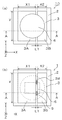
に対して接続電極3の側面3a2が障壁となり、光透過性樹脂8が側面3a2を越えるまで、光透過性樹脂8は反対側(図3(a)の矢印A)の方向に流れる量が多くなり、結果として、図3に実線で示すように、光透過性樹脂8は左右の形状が円形状(一点鎖線の絶縁部材9が有る場合の形状)からずれて変形しやすくなり、左右の形状が異なるドーム形状になりやすくなる。すなわち、光透過性樹脂8は、図3(c)に示すように、発光素子6の中央部に対して、X方向の負側に光透過性樹脂8が偏ったドーム形状になりやすくなる。また、光透過性樹脂8は、厚さが放射方向によって変動しやすくなる。このように、光透過性樹脂8のドーム状の曲面形状が変形することによって、発光装置は、例えば、青色LEDと黄色光を放射する蛍光体との組み合わせの場合には、放射角度(放射方向)により青色光と黄色光との割合がばらつくことになり、所望の色度の発光色を得ることが難しくなる。
部材9Aの間に空隙部2dを設けずに1つの絶縁部材で埋めている。これによって、発光素子6の下方に位置する空隙部2dを1つの絶縁部材で埋めてしまうので、空隙部2dに光透過性樹脂8が入り込まなくなる。また、発光素子搭載用基板1Aは、発光素子6の発熱量の大きい領域が1つの絶縁部材を介して接続電極3Bに連結されることになるので、発光素子6で生じた熱は絶縁部材9を経由して接続電極3Bに伝わり接続電極3Bを介して外部に放熱性されやすくなり、放熱性が向上することになる。
の変更および改良が可能である。
2 絶縁基体
2a 搭載部
3 接続電極
3a1、3a2 側面
4 内部配線
5 外部接続端子
6 発光素子
6a 電極
7 バンプ
8 光透過性樹脂
9、9A、9B 絶縁部材
10、10A、10B 発光装置
Claims (2)
- 絶縁基体と、
該絶縁基体の一方の主面に互いに側面が対向するように設けられた、平面視において互いに大きさが異なっている板状体の一対の接続電極と、
該一対の接続電極に搭載された発光素子と、
前記一対の接続電極の上面に延在されているとともに前記発光素子を埋設するように設けられている、蛍光体を含有する光透過性樹脂とを備えており、
前記一対の接続電極が対向する部位において、前記側面の間にわたって2つの絶縁部材が設けられており、該2つの絶縁部材は、平面視において前記発光素子の外縁部に重なっており、前記2つの絶縁部材の間に空隙部が設けられていることを特徴とする発光装置。 - 前記2つの絶縁部材は、端部が前記光透過性樹脂の延在部よりも外側に位置するように設けられていることを特徴とする請求項1に記載の発光装置。
Priority Applications (1)
| Application Number | Priority Date | Filing Date | Title |
|---|---|---|---|
| JP2013195510A JP6181492B2 (ja) | 2013-09-20 | 2013-09-20 | 発光装置 |
Applications Claiming Priority (1)
| Application Number | Priority Date | Filing Date | Title |
|---|---|---|---|
| JP2013195510A JP6181492B2 (ja) | 2013-09-20 | 2013-09-20 | 発光装置 |
Publications (2)
| Publication Number | Publication Date |
|---|---|
| JP2015061030A JP2015061030A (ja) | 2015-03-30 |
| JP6181492B2 true JP6181492B2 (ja) | 2017-08-16 |
Family
ID=52818295
Family Applications (1)
| Application Number | Title | Priority Date | Filing Date |
|---|---|---|---|
| JP2013195510A Expired - Fee Related JP6181492B2 (ja) | 2013-09-20 | 2013-09-20 | 発光装置 |
Country Status (1)
| Country | Link |
|---|---|
| JP (1) | JP6181492B2 (ja) |
Family Cites Families (1)
| Publication number | Priority date | Publication date | Assignee | Title |
|---|---|---|---|---|
| EP1670073B1 (en) * | 2003-09-30 | 2014-07-02 | Kabushiki Kaisha Toshiba | Light emitting device |
-
2013
- 2013-09-20 JP JP2013195510A patent/JP6181492B2/ja not_active Expired - Fee Related
Also Published As
| Publication number | Publication date |
|---|---|
| JP2015061030A (ja) | 2015-03-30 |
Similar Documents
| Publication | Publication Date | Title |
|---|---|---|
| JP5873108B2 (ja) | 配線基板および電子装置 | |
| JP2008288536A (ja) | 表面実装型セラミック基板 | |
| JP2008109079A (ja) | 表面実装型発光素子用配線基板および発光装置 | |
| JP2009054893A (ja) | 発光装置 | |
| JP6128367B2 (ja) | 発光装置、および配線基板の製造方法 | |
| JP2008218761A (ja) | 発光素子収納用パッケージ | |
| JP2011233775A (ja) | 半導体パッケージおよび半導体発光装置 | |
| CN102918666B (zh) | 发光装置 | |
| JP6224449B2 (ja) | 発光素子搭載用基板およびそれを備えた発光装置 | |
| CN107690714B (zh) | 发光元件搭载用基板、发光装置以及发光模块 | |
| JP2014157949A (ja) | 配線基板および電子装置 | |
| JP2009038161A (ja) | 発光素子収納用パッケージ | |
| CN108028232B (zh) | 布线基板、电子装置以及电子模块 | |
| JP2010067902A (ja) | 発光装置 | |
| JP2014116411A (ja) | 発光素子搭載用基板および発光装置 | |
| JP6181492B2 (ja) | 発光装置 | |
| JP2014045169A (ja) | 電子部品搭載用基板およびその製造方法 | |
| JP6306492B2 (ja) | 配線基板および電子装置 | |
| JP2008147513A (ja) | 発光装置 | |
| JP2009099823A (ja) | 発光装置 | |
| JP6668656B2 (ja) | パッケージ、発光装置、発光モジュール、及び、パッケージの製造方法 | |
| JP6235272B2 (ja) | 半導体素子搭載用基板およびそれを備えた半導体装置 | |
| JP2012160528A (ja) | 半導体パッケージ | |
| JP2011114172A (ja) | 発光素子搭載用基板および発光装置 | |
| JP5809440B2 (ja) | Ledモジュール |
Legal Events
| Date | Code | Title | Description |
|---|---|---|---|
| A621 | Written request for application examination |
Free format text: JAPANESE INTERMEDIATE CODE: A621 Effective date: 20160415 |
|
| A977 | Report on retrieval |
Free format text: JAPANESE INTERMEDIATE CODE: A971007 Effective date: 20170127 |
|
| A131 | Notification of reasons for refusal |
Free format text: JAPANESE INTERMEDIATE CODE: A131 Effective date: 20170228 |
|
| A521 | Request for written amendment filed |
Free format text: JAPANESE INTERMEDIATE CODE: A523 Effective date: 20170428 |
|
| TRDD | Decision of grant or rejection written | ||
| A01 | Written decision to grant a patent or to grant a registration (utility model) |
Free format text: JAPANESE INTERMEDIATE CODE: A01 Effective date: 20170620 |
|
| A61 | First payment of annual fees (during grant procedure) |
Free format text: JAPANESE INTERMEDIATE CODE: A61 Effective date: 20170720 |
|
| R150 | Certificate of patent or registration of utility model |
Ref document number: 6181492 Country of ref document: JP Free format text: JAPANESE INTERMEDIATE CODE: R150 |
|
| LAPS | Cancellation because of no payment of annual fees |