JP6200582B2 - 配線体及び配線基板 - Google Patents
配線体及び配線基板 Download PDFInfo
- Publication number
- JP6200582B2 JP6200582B2 JP2016512755A JP2016512755A JP6200582B2 JP 6200582 B2 JP6200582 B2 JP 6200582B2 JP 2016512755 A JP2016512755 A JP 2016512755A JP 2016512755 A JP2016512755 A JP 2016512755A JP 6200582 B2 JP6200582 B2 JP 6200582B2
- Authority
- JP
- Japan
- Prior art keywords
- disconnection
- wiring body
- wiring
- detection electrode
- electrode
- Prior art date
- Legal status (The legal status is an assumption and is not a legal conclusion. Google has not performed a legal analysis and makes no representation as to the accuracy of the status listed.)
- Expired - Fee Related
Links
Images





Classifications
-
- G—PHYSICS
- G06—COMPUTING OR CALCULATING; COUNTING
- G06F—ELECTRIC DIGITAL DATA PROCESSING
- G06F3/00—Input arrangements for transferring data to be processed into a form capable of being handled by the computer; Output arrangements for transferring data from processing unit to output unit, e.g. interface arrangements
- G06F3/01—Input arrangements or combined input and output arrangements for interaction between user and computer
- G06F3/03—Arrangements for converting the position or the displacement of a member into a coded form
- G06F3/041—Digitisers, e.g. for touch screens or touch pads, characterised by the transducing means
- G06F3/047—Digitisers, e.g. for touch screens or touch pads, characterised by the transducing means using sets of wires, e.g. crossed wires
-
- G—PHYSICS
- G06—COMPUTING OR CALCULATING; COUNTING
- G06F—ELECTRIC DIGITAL DATA PROCESSING
- G06F3/00—Input arrangements for transferring data to be processed into a form capable of being handled by the computer; Output arrangements for transferring data from processing unit to output unit, e.g. interface arrangements
- G06F3/01—Input arrangements or combined input and output arrangements for interaction between user and computer
- G06F3/03—Arrangements for converting the position or the displacement of a member into a coded form
- G06F3/041—Digitisers, e.g. for touch screens or touch pads, characterised by the transducing means
- G06F3/044—Digitisers, e.g. for touch screens or touch pads, characterised by the transducing means by capacitive means
- G06F3/0445—Digitisers, e.g. for touch screens or touch pads, characterised by the transducing means by capacitive means using two or more layers of sensing electrodes, e.g. using two layers of electrodes separated by a dielectric layer
-
- G—PHYSICS
- G06—COMPUTING OR CALCULATING; COUNTING
- G06F—ELECTRIC DIGITAL DATA PROCESSING
- G06F3/00—Input arrangements for transferring data to be processed into a form capable of being handled by the computer; Output arrangements for transferring data from processing unit to output unit, e.g. interface arrangements
- G06F3/01—Input arrangements or combined input and output arrangements for interaction between user and computer
- G06F3/03—Arrangements for converting the position or the displacement of a member into a coded form
- G06F3/041—Digitisers, e.g. for touch screens or touch pads, characterised by the transducing means
-
- G—PHYSICS
- G06—COMPUTING OR CALCULATING; COUNTING
- G06F—ELECTRIC DIGITAL DATA PROCESSING
- G06F3/00—Input arrangements for transferring data to be processed into a form capable of being handled by the computer; Output arrangements for transferring data from processing unit to output unit, e.g. interface arrangements
- G06F3/01—Input arrangements or combined input and output arrangements for interaction between user and computer
- G06F3/03—Arrangements for converting the position or the displacement of a member into a coded form
- G06F3/041—Digitisers, e.g. for touch screens or touch pads, characterised by the transducing means
- G06F3/044—Digitisers, e.g. for touch screens or touch pads, characterised by the transducing means by capacitive means
- G06F3/0446—Digitisers, e.g. for touch screens or touch pads, characterised by the transducing means by capacitive means using a grid-like structure of electrodes in at least two directions, e.g. using row and column electrodes
-
- G—PHYSICS
- G06—COMPUTING OR CALCULATING; COUNTING
- G06F—ELECTRIC DIGITAL DATA PROCESSING
- G06F2203/00—Indexing scheme relating to G06F3/00 - G06F3/048
- G06F2203/041—Indexing scheme relating to G06F3/041 - G06F3/045
- G06F2203/04103—Manufacturing, i.e. details related to manufacturing processes specially suited for touch sensitive devices
-
- G—PHYSICS
- G06—COMPUTING OR CALCULATING; COUNTING
- G06F—ELECTRIC DIGITAL DATA PROCESSING
- G06F2203/00—Indexing scheme relating to G06F3/00 - G06F3/048
- G06F2203/041—Indexing scheme relating to G06F3/041 - G06F3/045
- G06F2203/04112—Electrode mesh in capacitive digitiser: electrode for touch sensing is formed of a mesh of very fine, normally metallic, interconnected lines that are almost invisible to see. This provides a quite large but transparent electrode surface, without need for ITO or similar transparent conductive material
Landscapes
- Engineering & Computer Science (AREA)
- General Engineering & Computer Science (AREA)
- Theoretical Computer Science (AREA)
- Human Computer Interaction (AREA)
- Physics & Mathematics (AREA)
- General Physics & Mathematics (AREA)
- Position Input By Displaying (AREA)
- Structure Of Printed Boards (AREA)
Description
文献の参照による組み込みが認められる指定国については、2014年4月8日に日本国に出願された特願2014−079240号に記載された内容を参照により本明細書に組み込み、本明細書の記載の一部とする。
W2×5≧L2・・・(1)
但し、上記(1)式において、L2は前記第2の断線部の長さであり、W2は前記第2の細線の幅である。
|A1―A2|≦1・・・(2)
但し、上記(2)式において、A1は前記検出電極の開口率であり、A2は前記ダミー電極の開口率である。
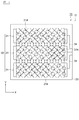
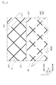
図1は本発明の第1実施形態における配線基板を示す平面図、図2は図1のII部の拡大平面図、図3は図2のIII-III線に沿った断面図、図4は図1において第1及び第2の断線部をマーキングした図である。
図6は本発明の第2実施形態における配線基板を示す平面図、図7は図6のVII部の拡大平面図、図8は図6において第1〜第3の断線部をマーキングした平面図である。
図10は本発明の第3実施形態における配線基板を示す平面図、図11は図10のXI部の拡大平面図である。
W2×5≧L2・・・(1)
但し、上記(1)式において、L2は第2の断線部355B’’の長さであり、W2は第2の細線351’’,352’’の幅である。
|A1―A2|≦1・・・(2)
但し、上記(2)式において、A1は検出電極31の開口率であり、A2はダミー電極35’’の開口率である。
|A1―A2|≦0.5・・・(3)
5…カバー部材
10,10A,10B,10’,10’’…配線基板
20…透明基板
21…上面
11’’…配線体
30,30A,30B,30’,30’’…導体パターン
31,31A,31B…検出電極
311,312…第1の細線
313…単位網目
314…第1の断線部
315…交点
316…辺
32…端部接続線
33,33A,33B…引出線
34…第3の断線部
35,35’,35’’…ダミー電極
351,351’’,352,352’’…第2の細線
353,353’’…単位網目
354…交点
355,355B,355B’’…第2の断線部
356…交点
50…接着層
51…支持部
52…平伏部
40…駆動回路
60…凹版
61…凹部
70…導電性材料
80…接着材料
Claims (12)
- 絶縁層と、
前記絶縁層上に設けられた導体パターンと、を備えた配線体であって、
前記導体パターンは、相互に並べられた複数の検出電極を備え、
前記検出電極は、複数の第1の細線を相互に交差させてなる網目状の検出電極であり、
前記検出電極は、前記第1の細線における交点以外の箇所に形成された第1の断線部を含み、
前記第1の断線部は、前記第1の細線における前記交点間の辺に形成され、
一方の前記交点と前記第1の断線部との間に前記辺の残部が存在していると共に、他方の交点と前記第1の断線部との間にも前記辺の残部が存在していることを特徴とする配線体。 - 請求項1に記載の配線体であって、
前記導体パターンは、複数の前記検出電極の間にそれぞれ介在し、複数の第2の細線を交差させてなる少なくとも一つの網目状のダミー電極を備えており、
前記ダミー電極は、少なくとも一つの第2の断線部を含むことを特徴とする配線体。 - 請求項2に記載の配線体であって、
前記ダミー電極は、前記検出電極を構成する単位網目と実質的に同一の形状の単位網目から構成されていることを特徴とする配線体。 - 請求項3に記載の配線体であって、
前記検出電極を構成する単位網目と、前記ダミー電極を構成する単位網目とは、前記検出電極及び前記ダミー電極の並設方向に対して垂直な方向において相互にずれていることを特徴とする配線体。 - 請求項2〜4の何れか1項に記載の配線体であって、
前記第2の断線部の長さが、前記第2の細線の幅に対して相対的に大きいことを特徴とする配線体。 - 請求項5に記載の配線体であって、
下記(1)式を満たすことを特徴とする配線体。
W2×5≧L2・・・(1)
但し、上記(1)式において、L2は前記第2の断線部の長さであり、W2は前記第2の細線の幅である。 - 請求項2〜6の何れか1項に記載の配線体であって、
下記(2)式を満たすことを特徴とする配線体。
|A1―A2|≦1・・・(2)
但し、上記(2)式において、A1は前記検出電極の開口率であり、A2は前記ダミー電極の開口率である。 - 請求項1〜7の何れか1項に記載の配線体であって、
前記第1の断線部は、前記第1の細線における前記交点間の前記辺の中央に形成されていることを特徴とする配線体。 - 請求項1〜8の何れか1項に記載の配線体であって、
前記検出電極を構成する一つの単位網目に対して、一つの前記第1の断線部が形成されていることを特徴とする配線体。 - 請求項1に記載の配線体であって、
前記導体パターンは、相互に隣り合う前記検出電極の前記第1の細線の交点に形成された少なくとも一つの第3の断線部を備えていることを特徴とする配線体。 - 請求項2〜7のいずれか1項に記載の配線体であって、
前記導体パターンは、相互に隣り合う前記検出電極と前記ダミー電極の前記第1及び前記第2の細線の交点に形成された少なくとも一つの第3の断線部をさらに備えることを特徴とする配線体。 - 請求項1〜11の何れか1項に記載の配線体を備える配線基板であって、
前記絶縁層は、前記導体パターンを支持する基材、または、前記導体パターンと基材を接着する接着層を構成することを特徴とする配線基板。
Applications Claiming Priority (3)
| Application Number | Priority Date | Filing Date | Title |
|---|---|---|---|
| JP2014079240 | 2014-04-08 | ||
| JP2014079240 | 2014-04-08 | ||
| PCT/JP2015/060974 WO2015156316A1 (ja) | 2014-04-08 | 2015-04-08 | 配線体及び配線基板 |
Publications (2)
| Publication Number | Publication Date |
|---|---|
| JPWO2015156316A1 JPWO2015156316A1 (ja) | 2017-04-13 |
| JP6200582B2 true JP6200582B2 (ja) | 2017-09-20 |
Family
ID=54287890
Family Applications (1)
| Application Number | Title | Priority Date | Filing Date |
|---|---|---|---|
| JP2016512755A Expired - Fee Related JP6200582B2 (ja) | 2014-04-08 | 2015-04-08 | 配線体及び配線基板 |
Country Status (6)
| Country | Link |
|---|---|
| US (1) | US10025444B2 (ja) |
| EP (1) | EP3130992A4 (ja) |
| JP (1) | JP6200582B2 (ja) |
| CN (1) | CN106133668B (ja) |
| TW (1) | TWI610600B (ja) |
| WO (1) | WO2015156316A1 (ja) |
Families Citing this family (29)
| Publication number | Priority date | Publication date | Assignee | Title |
|---|---|---|---|---|
| WO2017002609A1 (ja) * | 2015-06-29 | 2017-01-05 | 三菱製紙株式会社 | 光透過性導電材料 |
| TWI583748B (zh) * | 2016-02-25 | 2017-05-21 | 財團法人工業技術研究院 | 線路印刷裝置、線路印刷方法以及以印刷方法製造的線路結構 |
| JP6642113B2 (ja) * | 2016-02-29 | 2020-02-05 | トッパン・フォームズ株式会社 | 印刷方法、印刷装置 |
| JP6143909B1 (ja) * | 2016-03-29 | 2017-06-07 | 株式会社フジクラ | 配線体、配線基板、タッチセンサ、及び配線体の製造方法 |
| CN108700965A (zh) * | 2016-03-30 | 2018-10-23 | 株式会社藤仓 | 布线体、布线基板以及接触式传感器 |
| KR101929281B1 (ko) | 2016-05-19 | 2019-03-15 | 삼성디스플레이 주식회사 | 전자 장치 |
| US20190327829A1 (en) * | 2016-07-12 | 2019-10-24 | Fujikura Ltd. | Stretchable board |
| GB201613051D0 (en) * | 2016-07-28 | 2016-09-14 | Landa Labs (2012) Ltd | Applying an electrical conductor to a substrate |
| US12446160B2 (en) * | 2016-07-28 | 2025-10-14 | Landa Labs (2012) Ltd. | Application of electrical conductors to an electrically insulating substrate |
| EP3564800A1 (en) * | 2016-12-28 | 2019-11-06 | Fujikura Ltd. | Wiring body, wiring board and touch sensor |
| TWI652604B (zh) | 2017-02-16 | 2019-03-01 | 日商阿爾普士電氣股份有限公司 | 靜電感測器及輸入裝置 |
| JP6518384B2 (ja) * | 2017-03-06 | 2019-05-22 | 富士フイルム株式会社 | タッチパネル、タッチパネル用導電性シートおよびタッチセンサ |
| CN111251772B (zh) * | 2017-07-26 | 2021-04-09 | 丁蒙蒙 | 一种沙画表演设备 |
| JP2019079133A (ja) * | 2017-10-20 | 2019-05-23 | 日本航空電子工業株式会社 | タッチパネル |
| TWI905068B (zh) * | 2017-11-29 | 2025-11-11 | 日商大日本印刷股份有限公司 | 配線基板 |
| CN110007808B (zh) | 2017-12-29 | 2022-10-18 | 乐金显示有限公司 | 包括触摸传感器的电致发光显示器 |
| JP2019174860A (ja) * | 2018-03-26 | 2019-10-10 | 株式会社Vtsタッチセンサー | タッチパネル及び表示装置 |
| CN108563364B (zh) * | 2018-04-28 | 2024-03-08 | 京东方科技集团股份有限公司 | 一种触摸屏、其制作方法、触控显示面板及显示装置 |
| KR101952770B1 (ko) * | 2018-08-02 | 2019-02-27 | 동우 화인켐 주식회사 | 터치 센서 |
| KR102561107B1 (ko) | 2018-09-21 | 2023-07-27 | 엘지디스플레이 주식회사 | 터치표시장치 |
| KR102147439B1 (ko) * | 2018-10-17 | 2020-08-24 | 동우 화인켐 주식회사 | 안테나-데코 필름 적층체 및 이를 포함하는 디스플레이 장치 |
| CN109669576B (zh) * | 2018-12-25 | 2022-04-15 | 业成科技(成都)有限公司 | 触控模组 |
| JP2020194215A (ja) * | 2019-05-24 | 2020-12-03 | 日本航空電子工業株式会社 | タッチパネル |
| CN111651094B (zh) * | 2020-06-29 | 2023-07-28 | 合肥鑫晟光电科技有限公司 | 触控基板及触控显示装置 |
| JP7266955B2 (ja) * | 2021-05-20 | 2023-05-01 | Nissha株式会社 | 導電シート、タッチセンサ及びタッチセンサの製造方法 |
| CN113934325A (zh) * | 2021-10-14 | 2022-01-14 | 安徽精卓光显技术有限责任公司 | 一种金属网结构及触控屏 |
| WO2023188080A1 (ja) * | 2022-03-30 | 2023-10-05 | シャープディスプレイテクノロジー株式会社 | タッチセンサ、表示装置 |
| WO2024055300A1 (zh) * | 2022-09-16 | 2024-03-21 | 京东方科技集团股份有限公司 | 一种触控层、触控基板及触控显示装置 |
| KR20250016626A (ko) * | 2023-07-20 | 2025-02-04 | 삼성디스플레이 주식회사 | 터치 센서를 포함하는 표시 장치 |
Family Cites Families (16)
| Publication number | Priority date | Publication date | Assignee | Title |
|---|---|---|---|---|
| JP4610416B2 (ja) * | 2005-06-10 | 2011-01-12 | 日本写真印刷株式会社 | 静電容量型タッチパネル |
| JP5253288B2 (ja) | 2009-05-08 | 2013-07-31 | グンゼ株式会社 | 面状体及びタッチスイッチ |
| CN104635983B (zh) | 2008-07-31 | 2018-01-30 | 郡是株式会社 | 触摸开关 |
| JP5230533B2 (ja) | 2009-05-29 | 2013-07-10 | 三菱電機株式会社 | タッチパネルおよびそれを備えた表示装置 |
| JP5174745B2 (ja) * | 2009-06-09 | 2013-04-03 | グンゼ株式会社 | タッチスイッチ |
| JP2011059771A (ja) * | 2009-09-07 | 2011-03-24 | Hitachi Chem Co Ltd | 網目状導電性パターン、導体層パターン付き基材及びタッチパネル部材 |
| JP2011059772A (ja) * | 2009-09-07 | 2011-03-24 | Hitachi Chem Co Ltd | 網目状導電性パターン、導体層パターン付き基材及びタッチパネル部材 |
| KR101633034B1 (ko) * | 2009-10-23 | 2016-06-24 | 삼성디스플레이 주식회사 | 터치 기판, 이의 제조 방법 및 이를 갖는 표시 장치 |
| US8599150B2 (en) * | 2009-10-29 | 2013-12-03 | Atmel Corporation | Touchscreen electrode configuration |
| JP5667938B2 (ja) | 2010-09-30 | 2015-02-12 | 富士フイルム株式会社 | 静電容量方式タッチパネル |
| TWI567912B (zh) * | 2011-02-18 | 2017-01-21 | 富士軟片股份有限公司 | 導電片以及觸控面板 |
| WO2012115091A1 (ja) | 2011-02-24 | 2012-08-30 | 富士フイルム株式会社 | 導電シート及びタッチパネル |
| CN103984461B (zh) | 2011-12-16 | 2017-09-15 | 富士胶片株式会社 | 导电片以及触摸面板 |
| JP5875484B2 (ja) | 2011-12-22 | 2016-03-02 | 富士フイルム株式会社 | 導電シート及びタッチパネル |
| JP5892419B2 (ja) | 2012-01-11 | 2016-03-23 | 大日本印刷株式会社 | タッチパネルセンサ |
| CN103425366B (zh) * | 2013-02-04 | 2016-08-03 | 南昌欧菲光科技有限公司 | 引线电极及其制备方法 |
-
2015
- 2015-04-08 JP JP2016512755A patent/JP6200582B2/ja not_active Expired - Fee Related
- 2015-04-08 EP EP15776277.4A patent/EP3130992A4/en not_active Withdrawn
- 2015-04-08 TW TW104111195A patent/TWI610600B/zh not_active IP Right Cessation
- 2015-04-08 WO PCT/JP2015/060974 patent/WO2015156316A1/ja not_active Ceased
- 2015-04-08 CN CN201580016833.XA patent/CN106133668B/zh not_active Expired - Fee Related
- 2015-04-08 US US15/128,810 patent/US10025444B2/en not_active Expired - Fee Related
Also Published As
| Publication number | Publication date |
|---|---|
| EP3130992A1 (en) | 2017-02-15 |
| TWI610600B (zh) | 2018-01-01 |
| EP3130992A4 (en) | 2018-01-17 |
| US10025444B2 (en) | 2018-07-17 |
| TW201607386A (zh) | 2016-02-16 |
| CN106133668B (zh) | 2019-03-26 |
| CN106133668A (zh) | 2016-11-16 |
| WO2015156316A1 (ja) | 2015-10-15 |
| US20170102804A1 (en) | 2017-04-13 |
| JPWO2015156316A1 (ja) | 2017-04-13 |
Similar Documents
| Publication | Publication Date | Title |
|---|---|---|
| JP6200582B2 (ja) | 配線体及び配線基板 | |
| TWI657365B (zh) | Wiring body, wiring board, and touch detector | |
| TW201013488A (en) | Planar element, and touch switch | |
| JP6346584B2 (ja) | タッチパネルおよびその製造方法 | |
| CN104571740A (zh) | 触控面板及其制造方法 | |
| JP6084117B2 (ja) | タッチパネル、表示装置及び電子機器 | |
| US20200064971A1 (en) | Wiring body assembly, wiring board, and touch sensor | |
| JP5878593B2 (ja) | 入力装置の製造方法 | |
| JP6085647B2 (ja) | 配線体アセンブリ、導体層付き構造体、及びタッチセンサ | |
| CN203376709U (zh) | 触控面板 | |
| JP6180174B2 (ja) | タッチパネル、表示装置及び電子機器 | |
| KR20160042617A (ko) | 전도성 필름 및 이의 제조 방법, 그리고 전도성 필름을 포함하는 터치 패널 및 디스플레이 장치 | |
| JP2014112356A (ja) | タッチパネル | |
| JP6207555B2 (ja) | 配線体、導体層付き構造体、及びタッチセンサ | |
| WO2018181175A1 (ja) | 配線体、配線基板、及びタッチセンサ | |
| JP6440526B2 (ja) | 配線体 | |
| JP6549942B2 (ja) | 配線体、配線基板、及びタッチセンサ | |
| JP6034932B1 (ja) | 配線体、配線基板、及びタッチセンサ | |
| JP2020091582A (ja) | 配線体、配線板、及びタッチセンサ | |
| JP2020064403A (ja) | 配線体、配線板、及びタッチセンサ | |
| JP2018124615A (ja) | 配線体、配線基板、及びタッチセンサ | |
| JP2018110153A (ja) | 配線体アセンブリ、配線基板、及びタッチセンサ | |
| JP2020166326A (ja) | 配線体、配線板、タッチセンサ、及び、配線体の製造方法 | |
| JP2020047173A (ja) | 配線体、配線板、及びタッチセンサ | |
| JP2018110152A (ja) | 配線体アセンブリ、配線基板、及びタッチセンサ |
Legal Events
| Date | Code | Title | Description |
|---|---|---|---|
| A131 | Notification of reasons for refusal |
Free format text: JAPANESE INTERMEDIATE CODE: A131 Effective date: 20170221 |
|
| A601 | Written request for extension of time |
Free format text: JAPANESE INTERMEDIATE CODE: A601 Effective date: 20170419 |
|
| A521 | Request for written amendment filed |
Free format text: JAPANESE INTERMEDIATE CODE: A523 Effective date: 20170621 |
|
| TRDD | Decision of grant or rejection written | ||
| A01 | Written decision to grant a patent or to grant a registration (utility model) |
Free format text: JAPANESE INTERMEDIATE CODE: A01 Effective date: 20170815 |
|
| A61 | First payment of annual fees (during grant procedure) |
Free format text: JAPANESE INTERMEDIATE CODE: A61 Effective date: 20170825 |
|
| R151 | Written notification of patent or utility model registration |
Ref document number: 6200582 Country of ref document: JP Free format text: JAPANESE INTERMEDIATE CODE: R151 |
|
| LAPS | Cancellation because of no payment of annual fees |