JP6236073B2 - 検査装置、検査方法、および、制御装置 - Google Patents
検査装置、検査方法、および、制御装置 Download PDFInfo
- Publication number
- JP6236073B2 JP6236073B2 JP2015516867A JP2015516867A JP6236073B2 JP 6236073 B2 JP6236073 B2 JP 6236073B2 JP 2015516867 A JP2015516867 A JP 2015516867A JP 2015516867 A JP2015516867 A JP 2015516867A JP 6236073 B2 JP6236073 B2 JP 6236073B2
- Authority
- JP
- Japan
- Prior art keywords
- area
- region
- fluid
- circuit pattern
- target shape
- Prior art date
- Legal status (The legal status is an assumption and is not a legal conclusion. Google has not performed a legal analysis and makes no representation as to the accuracy of the status listed.)
- Active
Links
Images


Classifications
-
- B—PERFORMING OPERATIONS; TRANSPORTING
- B41—PRINTING; LINING MACHINES; TYPEWRITERS; STAMPS
- B41J—TYPEWRITERS; SELECTIVE PRINTING MECHANISMS, i.e. MECHANISMS PRINTING OTHERWISE THAN FROM A FORME; CORRECTION OF TYPOGRAPHICAL ERRORS
- B41J2/00—Typewriters or selective printing mechanisms characterised by the printing or marking process for which they are designed
- B41J2/005—Typewriters or selective printing mechanisms characterised by the printing or marking process for which they are designed characterised by bringing liquid or particles selectively into contact with a printing material
- B41J2/01—Ink jet
- B41J2/21—Ink jet for multi-colour printing
- B41J2/2132—Print quality control characterised by dot disposition, e.g. for reducing white stripes or banding
- B41J2/2142—Detection of malfunctioning nozzles
-
- G—PHYSICS
- G01—MEASURING; TESTING
- G01N—INVESTIGATING OR ANALYSING MATERIALS BY DETERMINING THEIR CHEMICAL OR PHYSICAL PROPERTIES
- G01N21/00—Investigating or analysing materials by the use of optical means, i.e. using sub-millimetre waves, infrared, visible or ultraviolet light
- G01N21/84—Systems specially adapted for particular applications
- G01N21/88—Investigating the presence of flaws or contamination
- G01N21/95—Investigating the presence of flaws or contamination characterised by the material or shape of the object to be examined
- G01N21/956—Inspecting patterns on the surface of objects
- G01N21/95607—Inspecting patterns on the surface of objects using a comparative method
-
- G—PHYSICS
- G01—MEASURING; TESTING
- G01N—INVESTIGATING OR ANALYSING MATERIALS BY DETERMINING THEIR CHEMICAL OR PHYSICAL PROPERTIES
- G01N21/00—Investigating or analysing materials by the use of optical means, i.e. using sub-millimetre waves, infrared, visible or ultraviolet light
- G01N21/84—Systems specially adapted for particular applications
- G01N21/88—Investigating the presence of flaws or contamination
- G01N21/95—Investigating the presence of flaws or contamination characterised by the material or shape of the object to be examined
- G01N21/956—Inspecting patterns on the surface of objects
- G01N21/95684—Patterns showing highly reflecting parts, e.g. metallic elements
-
- H—ELECTRICITY
- H05—ELECTRIC TECHNIQUES NOT OTHERWISE PROVIDED FOR
- H05K—PRINTED CIRCUITS; CASINGS OR CONSTRUCTIONAL DETAILS OF ELECTRIC APPARATUS; MANUFACTURE OF ASSEMBLAGES OF ELECTRICAL COMPONENTS
- H05K3/00—Apparatus or processes for manufacturing printed circuits
- H05K3/10—Apparatus or processes for manufacturing printed circuits in which conductive material is applied to the insulating support in such a manner as to form the desired conductive pattern
- H05K3/12—Apparatus or processes for manufacturing printed circuits in which conductive material is applied to the insulating support in such a manner as to form the desired conductive pattern using thick film techniques, e.g. printing techniques to apply the conductive material or similar techniques for applying conductive paste or ink patterns
- H05K3/1241—Apparatus or processes for manufacturing printed circuits in which conductive material is applied to the insulating support in such a manner as to form the desired conductive pattern using thick film techniques, e.g. printing techniques to apply the conductive material or similar techniques for applying conductive paste or ink patterns by ink-jet printing or drawing by dispensing
- H05K3/125—Apparatus or processes for manufacturing printed circuits in which conductive material is applied to the insulating support in such a manner as to form the desired conductive pattern using thick film techniques, e.g. printing techniques to apply the conductive material or similar techniques for applying conductive paste or ink patterns by ink-jet printing or drawing by dispensing by ink-jet printing
-
- H—ELECTRICITY
- H05—ELECTRIC TECHNIQUES NOT OTHERWISE PROVIDED FOR
- H05K—PRINTED CIRCUITS; CASINGS OR CONSTRUCTIONAL DETAILS OF ELECTRIC APPARATUS; MANUFACTURE OF ASSEMBLAGES OF ELECTRICAL COMPONENTS
- H05K2203/00—Indexing scheme relating to apparatus or processes for manufacturing printed circuits covered by H05K3/00
- H05K2203/01—Tools for processing; Objects used during processing
- H05K2203/0104—Tools for processing; Objects used during processing for patterning or coating
- H05K2203/013—Inkjet printing, e.g. for printing insulating material or resist
-
- H—ELECTRICITY
- H05—ELECTRIC TECHNIQUES NOT OTHERWISE PROVIDED FOR
- H05K—PRINTED CIRCUITS; CASINGS OR CONSTRUCTIONAL DETAILS OF ELECTRIC APPARATUS; MANUFACTURE OF ASSEMBLAGES OF ELECTRICAL COMPONENTS
- H05K2203/00—Indexing scheme relating to apparatus or processes for manufacturing printed circuits covered by H05K3/00
- H05K2203/16—Inspection; Monitoring; Aligning
- H05K2203/163—Monitoring a manufacturing process
-
- H—ELECTRICITY
- H05—ELECTRIC TECHNIQUES NOT OTHERWISE PROVIDED FOR
- H05K—PRINTED CIRCUITS; CASINGS OR CONSTRUCTIONAL DETAILS OF ELECTRIC APPARATUS; MANUFACTURE OF ASSEMBLAGES OF ELECTRICAL COMPONENTS
- H05K3/00—Apparatus or processes for manufacturing printed circuits
- H05K3/30—Assembling printed circuits with electric components, e.g. with resistors
- H05K3/32—Assembling printed circuits with electric components, e.g. with resistors electrically connecting electric components or wires to printed circuits
- H05K3/34—Assembling printed circuits with electric components, e.g. with resistors electrically connecting electric components or wires to printed circuits by soldering
- H05K3/3465—Application of solder
- H05K3/3485—Application of solder paste, slurry or powder
Landscapes
- Engineering & Computer Science (AREA)
- General Physics & Mathematics (AREA)
- Immunology (AREA)
- Physics & Mathematics (AREA)
- Pathology (AREA)
- Life Sciences & Earth Sciences (AREA)
- Chemical & Material Sciences (AREA)
- Analytical Chemistry (AREA)
- Biochemistry (AREA)
- Health & Medical Sciences (AREA)
- General Health & Medical Sciences (AREA)
- Microelectronics & Electronic Packaging (AREA)
- Manufacturing & Machinery (AREA)
- Quality & Reliability (AREA)
- Manufacturing Of Printed Wiring (AREA)
- Ink Jet (AREA)
- Accessory Devices And Overall Control Thereof (AREA)
- Investigating Materials By The Use Of Optical Means Adapted For Particular Applications (AREA)
- Image Processing (AREA)
- Coating Apparatus (AREA)
Description
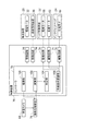
図1に、本発明の実施例の印刷装置10を示す。印刷装置10は、回路基板上に回路パターンを印刷するための装置である。印刷装置10は、搬送装置20と、ヘッド移動装置22と、インクジェットヘッド24とを備えている。
印刷装置10では、上述した構成によって、インクジェットヘッド24が搬送装置20に保持された回路基板34に銀ナノ粒子ペーストを吐出することで、回路基板34に回路パターンが形成される。具体的には、コントローラ72の指令により、回路基板34が作業位置まで搬送され、その位置において、回路基板34が、基板保持装置36によって固定的に保持される。そして、インクジェットヘッド24が、コントローラ72の指令により、回路基板34の所定の位置の上方に移動する。続いて、インクジェットヘッド24は、コントローラ72の指令により、回路基板34の上面に銀ナノ粒子ペーストを吐出し、回路パターンが印刷される。
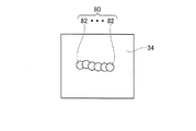
印刷装置10では、上述したように、インクジェットヘッド24の下面に形成された複数のノズル穴から銀ナノ粒子ペーストを吐出することで、回路パターンが印刷される。このため、図3に示すように、回路パターン80は、複数のドット状に吐出された銀ナノ粒子ペースト82によって、回路基板34上に形成される。このようにして形成された回路パターン80では、ドット状の銀ナノ粒子ペースト82の径、つまり、銀ナノ粒子ペースト82の吐出量等によって、銀ナノ粒子ペースト82と銀ナノ粒子ペースト82との間に隙間が生じる場合がある。このような場合には、電極間に形成される回路パターンが断線するため、好ましくない。また、銀ナノ粒子ペースト82が適切な位置に吐出されない場合等には、回路パターン80の長さが目標とする長さとならずに、電極と電極とを接続できない虞がある。
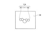
また、印刷装置10では、上記判定により、回路パターンの印刷精度が低いと判定された場合には、印刷条件が自動で調整される。具体的に、例えば、図7に示す形状の回路パターン110に対して、上記判定が行われる場合について説明する。回路パターン110では、図8に示すように、第1の矩形88の内部の領域、つまり、第1の領域のうちの銀ナノ粒子ペースト82が吐出されていない箇所の面積、つまり、第1の演算面積が、比較的小さく、第1の閾面積より小さい。このため、回路パターン110の長さが、目標形状86の長さより短いと想定され、印刷精度が低いと判定される。
Claims (3)
- 印刷媒体に目標形状となるように流体を吐出する流体吐出装置による印刷精度を検査する検査装置において、
当該検査装置が、
前記流体吐出装置によって流体が吐出された印刷媒体を撮像する撮像部と、
前記撮像部により撮像された画像の画像データに基づいて、印刷媒体の予め設定された設定領域のうちの流体が吐出されていない箇所の面積を演算する演算部と、
前記演算部により演算された面積と予め設定された閾面積との比較により、前記流体吐出装置による印刷精度の良否を判定する判定部と
を備え、
前記設定領域として、少なくとも前記目標形状全体を含む第1の領域と、少なくとも前記目標形状全体を除いた第2の領域と、前記目標形状内に納まる第3の領域と、が設定されており、
前記判定部は、
前記第1の領域を前記設定領域として前記演算部により演算された面積が第1の前記閾面積以下であり、前記第2の領域を前記設定領域として前記演算部により演算された面積が第2の前記閾面積以上であり、前記第3の領域を前記設定領域として前記演算部により演算された面積が第3の前記閾面積以下である際に、前記流体吐出装置による印刷精度が良好であると判定することを特徴とする検査装置。 - 印刷媒体に目標形状となるように流体を吐出する流体吐出装置の作動を制御する制御装置において、
当該制御装置が、
請求項1に記載の検査装置の判定部による判定結果に基づいて、前記流体吐出装置の作動条件を調整する作動条件調整部を備えることを特徴とする制御装置。 - 印刷媒体に目標形状となるように流体を吐出する流体吐出装置による印刷精度を検査する検査方法において、
当該検査方法が、
前記流体吐出装置によって流体が吐出された印刷媒体を撮像する撮像工程と、
前記撮像工程において撮像された画像の画像データに基づいて、印刷媒体の予め設定された設定領域のうちの流体が吐出されていない箇所の面積を演算する演算工程と、
前記演算工程において演算された面積と予め設定された閾面積との比較により、前記流体吐出装置による印刷精度の良否を判定する判定工程と
を含み、
前記設定領域として、少なくとも前記目標形状全体を含む第1の領域と、少なくとも前記目標形状全体を除いた第2の領域と、前記目標形状内に納まる第3の領域と、が設定されており、
前記判定工程は、
前記第1の領域を前記設定領域として前記演算工程において演算された面積が第1の前記閾面積以下であり、前記第2の領域を前記設定領域として前記演算工程において演算された面積が第2の前記閾面積以上であり、前記第3の領域を前記設定領域として前記演算工程において演算された面積が第3の前記閾面積以下である際に、前記流体吐出装置による印刷精度が良好であると判定することを特徴とする検査方法。
Applications Claiming Priority (1)
| Application Number | Priority Date | Filing Date | Title |
|---|---|---|---|
| PCT/JP2013/063837 WO2014184960A1 (ja) | 2013-05-17 | 2013-05-17 | 検査装置、検査方法、および、制御装置 |
Publications (2)
| Publication Number | Publication Date |
|---|---|
| JPWO2014184960A1 JPWO2014184960A1 (ja) | 2017-02-23 |
| JP6236073B2 true JP6236073B2 (ja) | 2017-11-22 |
Family
ID=51897965
Family Applications (1)
| Application Number | Title | Priority Date | Filing Date |
|---|---|---|---|
| JP2015516867A Active JP6236073B2 (ja) | 2013-05-17 | 2013-05-17 | 検査装置、検査方法、および、制御装置 |
Country Status (2)
| Country | Link |
|---|---|
| JP (1) | JP6236073B2 (ja) |
| WO (1) | WO2014184960A1 (ja) |
Cited By (1)
| Publication number | Priority date | Publication date | Assignee | Title |
|---|---|---|---|---|
| CN111604273A (zh) * | 2020-05-22 | 2020-09-01 | 深圳市周大福珠宝制造有限公司 | 珠宝印字质量检测设备、系统、方法及装置 |
Families Citing this family (2)
| Publication number | Priority date | Publication date | Assignee | Title |
|---|---|---|---|---|
| CN106847716A (zh) * | 2017-02-28 | 2017-06-13 | 上海图正信息科技股份有限公司 | 一种芯片封装工艺 |
| CN114485409A (zh) * | 2022-04-18 | 2022-05-13 | 深圳市元硕自动化科技有限公司 | 原料板质量检测方法、装置、设备及可读存储介质 |
Family Cites Families (8)
| Publication number | Priority date | Publication date | Assignee | Title |
|---|---|---|---|---|
| JPS61239105A (ja) * | 1985-04-17 | 1986-10-24 | Fuji Electric Co Ltd | 印刷パタ−ンの検査方法 |
| US5555316A (en) * | 1992-06-30 | 1996-09-10 | Matsushita Electric Industrial Co., Ltd. | Inspecting apparatus of mounting state of component or printing state of cream solder in mounting line of electronic component |
| JP3211385B2 (ja) * | 1992-07-08 | 2001-09-25 | 松下電器産業株式会社 | クリーム半田印刷検査方法 |
| JPH1086322A (ja) * | 1996-09-12 | 1998-04-07 | Opt Kk | クリームハンダ印刷検査方法およびその装置 |
| JP2008264608A (ja) * | 2007-04-16 | 2008-11-06 | Shibaura Mechatronics Corp | 液滴塗布装置及び液滴塗布方法 |
| JP2010192733A (ja) * | 2009-02-19 | 2010-09-02 | Seiko Epson Corp | 配線基板の製造方法および配線基板製造装置 |
| JP2010204408A (ja) * | 2009-03-04 | 2010-09-16 | Seiko Epson Corp | 液滴吐出装置、液滴吐出方法、及びカラーフィルターの製造方法 |
| JP5656249B2 (ja) * | 2010-11-12 | 2015-01-21 | 富士機械製造株式会社 | 粘性液状物塗布装置 |
-
2013
- 2013-05-17 JP JP2015516867A patent/JP6236073B2/ja active Active
- 2013-05-17 WO PCT/JP2013/063837 patent/WO2014184960A1/ja not_active Ceased
Cited By (1)
| Publication number | Priority date | Publication date | Assignee | Title |
|---|---|---|---|---|
| CN111604273A (zh) * | 2020-05-22 | 2020-09-01 | 深圳市周大福珠宝制造有限公司 | 珠宝印字质量检测设备、系统、方法及装置 |
Also Published As
| Publication number | Publication date |
|---|---|
| WO2014184960A1 (ja) | 2014-11-20 |
| JPWO2014184960A1 (ja) | 2017-02-23 |
Similar Documents
| Publication | Publication Date | Title |
|---|---|---|
| CN107053866B (zh) | 液体喷射设备,液体喷射系统及液体喷射方法 | |
| US10112269B2 (en) | Screen printer, component mounting line, and screen printing method | |
| US9233534B2 (en) | Droplet-discharging head, image-forming device, and method for positioning head modules of droplet-discharging head | |
| JP6695237B2 (ja) | 液滴吐出装置及び液滴吐出条件補正方法 | |
| KR101396216B1 (ko) | 잉크 접촉각 및 도포 상태 측정 시스템 및 방법, 및 이를 구비한 잉크젯 인쇄 장치 | |
| US8800440B2 (en) | Screen print system and method for cleaning a mask of the same | |
| US10682870B2 (en) | Conveyed object detector, conveyance device, device including movable head, conveyed object detecting method, and non-transitory recording medium storing program of same | |
| CN106605453B (zh) | 喷墨印刷系统和处理晶圆的方法 | |
| US8567314B2 (en) | Screen print system and method for cleaning a mask of the same | |
| JP6236073B2 (ja) | 検査装置、検査方法、および、制御装置 | |
| JP6251268B2 (ja) | 部品装着検査装置 | |
| EP3689627B1 (en) | Method for determining working gap, and recording device | |
| JP6109171B2 (ja) | 対基板作業システムおよび作業機 | |
| JP5845421B2 (ja) | 電子部品実装装置および転写膜厚検出方法 | |
| JP6475030B2 (ja) | 基板処理システム及び基板処理方法 | |
| JP4560683B2 (ja) | 導電性ボール配列装置 | |
| JP5092649B2 (ja) | 塗布剤の劣化検査装置及び劣化検査方法並びに劣化検査プログラム | |
| TW202321048A (zh) | 液體吐出裝置、吐出狀態評價方法、資訊處理裝置及印刷基板之製造方法 | |
| JP2012135990A (ja) | 画像記録装置の記録ヘッドの取り付け方法 | |
| JP2011136307A (ja) | パターン描画装置及びパターン描画方法 | |
| CN111093996A (zh) | 丝网印刷机 | |
| JP2010036488A (ja) | 液滴吐出装置 | |
| CN110087885B (zh) | 丝网印刷机 | |
| JP2023173295A (ja) | 部品実装システム | |
| JP2019214133A (ja) | インクジェットプリンタ |
Legal Events
| Date | Code | Title | Description |
|---|---|---|---|
| A131 | Notification of reasons for refusal |
Free format text: JAPANESE INTERMEDIATE CODE: A131 Effective date: 20170321 |
|
| A521 | Request for written amendment filed |
Free format text: JAPANESE INTERMEDIATE CODE: A523 Effective date: 20170518 |
|
| TRDD | Decision of grant or rejection written | ||
| A01 | Written decision to grant a patent or to grant a registration (utility model) |
Free format text: JAPANESE INTERMEDIATE CODE: A01 Effective date: 20171017 |
|
| A61 | First payment of annual fees (during grant procedure) |
Free format text: JAPANESE INTERMEDIATE CODE: A61 Effective date: 20171027 |
|
| R150 | Certificate of patent or registration of utility model |
Ref document number: 6236073 Country of ref document: JP Free format text: JAPANESE INTERMEDIATE CODE: R150 |
|
| S533 | Written request for registration of change of name |
Free format text: JAPANESE INTERMEDIATE CODE: R313533 |
|
| R350 | Written notification of registration of transfer |
Free format text: JAPANESE INTERMEDIATE CODE: R350 |
|
| R250 | Receipt of annual fees |
Free format text: JAPANESE INTERMEDIATE CODE: R250 |
|
| R250 | Receipt of annual fees |
Free format text: JAPANESE INTERMEDIATE CODE: R250 |
|
| R250 | Receipt of annual fees |
Free format text: JAPANESE INTERMEDIATE CODE: R250 |
|
| R250 | Receipt of annual fees |
Free format text: JAPANESE INTERMEDIATE CODE: R250 |
|
| R250 | Receipt of annual fees |
Free format text: JAPANESE INTERMEDIATE CODE: R250 |
|
| R250 | Receipt of annual fees |
Free format text: JAPANESE INTERMEDIATE CODE: R250 |