JP6236367B2 - センサーモジュール及びセンサーモジュールの製造方法 - Google Patents
センサーモジュール及びセンサーモジュールの製造方法 Download PDFInfo
- Publication number
- JP6236367B2 JP6236367B2 JP2014163374A JP2014163374A JP6236367B2 JP 6236367 B2 JP6236367 B2 JP 6236367B2 JP 2014163374 A JP2014163374 A JP 2014163374A JP 2014163374 A JP2014163374 A JP 2014163374A JP 6236367 B2 JP6236367 B2 JP 6236367B2
- Authority
- JP
- Japan
- Prior art keywords
- region
- sensor
- circuit board
- printed circuit
- sensor module
- Prior art date
- Legal status (The legal status is an assumption and is not a legal conclusion. Google has not performed a legal analysis and makes no representation as to the accuracy of the status listed.)
- Expired - Fee Related
Links
- 238000004519 manufacturing process Methods 0.000 title description 26
- 238000004891 communication Methods 0.000 claims description 41
- 239000011347 resin Substances 0.000 claims description 39
- 229920005989 resin Polymers 0.000 claims description 39
- 238000000034 method Methods 0.000 claims description 15
- 239000000853 adhesive Substances 0.000 claims description 9
- 230000001070 adhesive effect Effects 0.000 claims description 9
- 239000000758 substrate Substances 0.000 claims description 9
- 230000003287 optical effect Effects 0.000 claims description 6
- 238000007789 sealing Methods 0.000 claims description 3
- 230000006866 deterioration Effects 0.000 description 10
- 230000035945 sensitivity Effects 0.000 description 10
- 125000006850 spacer group Chemical group 0.000 description 9
- 239000004020 conductor Substances 0.000 description 7
- 230000000694 effects Effects 0.000 description 2
- 229910000679 solder Inorganic materials 0.000 description 2
- 230000001133 acceleration Effects 0.000 description 1
- 238000005452 bending Methods 0.000 description 1
- 238000012986 modification Methods 0.000 description 1
- 230000004048 modification Effects 0.000 description 1
- 238000007639 printing Methods 0.000 description 1
- 238000005476 soldering Methods 0.000 description 1
Images



Landscapes
- Non-Metallic Protective Coatings For Printed Circuits (AREA)
- Structures For Mounting Electric Components On Printed Circuit Boards (AREA)
- Combinations Of Printed Boards (AREA)
Description
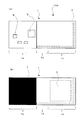
以下、本発明の実施形態について、図面を参照しながら説明する。尚、本明細書では、特に断りの無い限り、各図面のX1側を右側、X2側を左側、Y1側を奥側、Y2側を手前側、Z1側を上側、Z2側を下側として説明する。
次に、センサーモジュール100の製造方法について、図4及び図5を用いて説明する。
1a 第1の領域
1b 第2の領域
1c 第3の領域
1d リジッドフレキシブル基板
3 センサー
5 通信用電子部品
7 樹脂
9 アンテナ
11 接着剤
50 金型
100 センサーモジュール
Claims (8)
- 少なくとも一部が可撓性であるプリント基板と、前記プリント基板に搭載された通信用電子部品と、前記プリント基板に搭載されたセンサーと、を備え、
前記プリント基板が、第1の領域と、第2の領域と、前記第1の領域及び前記第2の領域それぞれの間に位置すると共に湾曲可能な可撓性を有している第3の領域と、を有し、
前記通信用電子部品が前記第1の領域の一方の面に実装されていると共に樹脂によって封止されており、前記センサーが前記第2の領域の他方の面に実装されていて、
前記第2の領域の前記一方の面と前記樹脂とが接触するように、前記第3の領域が折り曲げられていて、前記第2の領域の前記一方の面と前記樹脂とが接着されている、ことを特徴とするセンサーモジュール。 - 前記プリント基板が、可撓性を有する部分と、前記可撓性を有する部分より剛性の高い部分と、を備えたリジッドフレキシブル基板であって、
前記通信用電子部品が実装される第1の領域は、前記剛性の高い部分である、ことを特徴とする請求項1に記載のセンサーモジュール。 - 前記センサーが実装される第2の領域は、前記可撓性を有する部分である、ことを特徴とする請求項2に記載のセンサーモジュール。
- アンテナが、前記プリント基板の第2の領域の他方の面に前記センサーを避けて配設されている、ことを特徴とする請求項1乃至3請求項の何れかに記載のセンサーモジュール。
- 前記プリント基板が矩形状をしており、
前記アンテナは、前記プリント基板の第2の領域の、少なくとも2つの辺に沿って連続して設けられている、ことを特徴とする請求項4に記載のセンサーモジュール。 - 前記樹脂と前記プリント基板の第2の領域とが接着剤によって固定されている、ことを特徴とする請求項1乃至請求項5の何れかに記載のセンサーモジュール。
- 前記センサーは、磁気センサー、光センサー、ガスセンサー、温度センサー、湿度センサー、又は、気圧センサーの何れかであることを特徴とする請求項1乃至請求項6の何れかに記載のセンサーモジュール。
- 可撓性を有する部分と前記可撓性を有する部分より剛性の高い部分とを備えたプリント基板の、前記剛性の高い部分である第1の領域の一方の面に通信用電子部品を実装する工程と、
前記通信用電子部品を樹脂で封止する工程と、
前記プリント基板の可撓性を有する部分にある第2の領域の他方の面にセンサーを実装する工程と、
前記第1の領域及び前記第2の領域それぞれの間に位置すると共に可撓性を有する部分にある第3の領域を湾曲させて、前記樹脂と前記第2の領域の一方の面とを接着させる工程と、を有する、ことを特徴とするセンサーモジュールの製造方法。
Priority Applications (1)
| Application Number | Priority Date | Filing Date | Title |
|---|---|---|---|
| JP2014163374A JP6236367B2 (ja) | 2014-08-11 | 2014-08-11 | センサーモジュール及びセンサーモジュールの製造方法 |
Applications Claiming Priority (1)
| Application Number | Priority Date | Filing Date | Title |
|---|---|---|---|
| JP2014163374A JP6236367B2 (ja) | 2014-08-11 | 2014-08-11 | センサーモジュール及びセンサーモジュールの製造方法 |
Publications (2)
| Publication Number | Publication Date |
|---|---|
| JP2016039337A JP2016039337A (ja) | 2016-03-22 |
| JP6236367B2 true JP6236367B2 (ja) | 2017-11-22 |
Family
ID=55530148
Family Applications (1)
| Application Number | Title | Priority Date | Filing Date |
|---|---|---|---|
| JP2014163374A Expired - Fee Related JP6236367B2 (ja) | 2014-08-11 | 2014-08-11 | センサーモジュール及びセンサーモジュールの製造方法 |
Country Status (1)
| Country | Link |
|---|---|
| JP (1) | JP6236367B2 (ja) |
Families Citing this family (2)
| Publication number | Priority date | Publication date | Assignee | Title |
|---|---|---|---|---|
| WO2019009062A1 (ja) | 2017-07-07 | 2019-01-10 | 株式会社村田製作所 | 高周波電力回路モジュール |
| EP3714262B1 (en) | 2017-11-20 | 2025-10-01 | Honeywell International Inc. | Low-profile photoionization detector comprising a flexible substrate |
Family Cites Families (5)
| Publication number | Priority date | Publication date | Assignee | Title |
|---|---|---|---|---|
| US7005179B2 (en) * | 2002-07-26 | 2006-02-28 | The Regents Of The University Of California | Conductive inks for metalization in integrated polymer microsystems |
| US8276269B2 (en) * | 2008-06-20 | 2012-10-02 | Intel Corporation | Dual epoxy dielectric and photosensitive solder mask coatings, and processes of making same |
| US8979758B2 (en) * | 2010-06-29 | 2015-03-17 | Orthosensor Inc | Sensing module for orthopedic load sensing insert device |
| WO2012036139A1 (ja) * | 2010-09-14 | 2012-03-22 | 株式会社村田製作所 | リーダライタ用アンテナモジュールおよびアンテナ装置 |
| US9093360B2 (en) * | 2013-01-11 | 2015-07-28 | Analog Devices, Inc. | Compact device package |
-
2014
- 2014-08-11 JP JP2014163374A patent/JP6236367B2/ja not_active Expired - Fee Related
Also Published As
| Publication number | Publication date |
|---|---|
| JP2016039337A (ja) | 2016-03-22 |
Similar Documents
| Publication | Publication Date | Title |
|---|---|---|
| JP5465288B2 (ja) | 赤外線センサ | |
| CN101379869A (zh) | 屏蔽壳和具有屏蔽壳的微机电系统传声器 | |
| US7762819B2 (en) | Substrate connecting member and connecting structure | |
| JP4930566B2 (ja) | 中継基板、プリント基板ユニット、および、中継基板の製造方法 | |
| JP6102770B2 (ja) | 高周波モジュール | |
| JP6230124B2 (ja) | 撮像素子内蔵基板及びその製造方法、並びに撮像装置 | |
| JP2017011244A (ja) | 通信モジュール及び通信モジュールの製造方法 | |
| KR101772490B1 (ko) | 인쇄회로기판 어셈블리 | |
| US10187975B2 (en) | Multilayer substrate and electronic device | |
| JP6236367B2 (ja) | センサーモジュール及びセンサーモジュールの製造方法 | |
| WO2010097871A1 (ja) | 回路基板モジュール及びこれを備えた電子機器 | |
| JP4993383B2 (ja) | シール構造体 | |
| JPWO2012105394A1 (ja) | 電子部品モジュール、及び該電子部品モジュールを備える多機能カード | |
| JP6323622B2 (ja) | 部品実装基板 | |
| JP6998725B2 (ja) | 基板積層体、および、撮像装置 | |
| JP2008078205A (ja) | 基板組立体及びその製造方法、電子部品組立体及びその製造方法、電子装置 | |
| JP2001326428A (ja) | プリント基板 | |
| JP2007201263A (ja) | フレキシブル基板の取付構造 | |
| JP6089557B2 (ja) | 電子部品モジュール | |
| JP6168558B2 (ja) | 高周波モジュール、電子機器及び、高周波モジュールの製造方法 | |
| JPWO2009069236A1 (ja) | 回路基板モジュールおよび電子機器 | |
| JP2015053402A (ja) | 半導体装置とその製造方法、及び、半導体装置を搭載したアプリケーションボード | |
| WO2017006614A1 (ja) | 高周波モジュール | |
| US11952264B2 (en) | Electronic device | |
| JP2010103647A (ja) | 弾性表面波デバイス |
Legal Events
| Date | Code | Title | Description |
|---|---|---|---|
| A621 | Written request for application examination |
Free format text: JAPANESE INTERMEDIATE CODE: A621 Effective date: 20170106 |
|
| A977 | Report on retrieval |
Free format text: JAPANESE INTERMEDIATE CODE: A971007 Effective date: 20170927 |
|
| TRDD | Decision of grant or rejection written | ||
| A01 | Written decision to grant a patent or to grant a registration (utility model) |
Free format text: JAPANESE INTERMEDIATE CODE: A01 Effective date: 20171024 |
|
| A61 | First payment of annual fees (during grant procedure) |
Free format text: JAPANESE INTERMEDIATE CODE: A61 Effective date: 20171030 |
|
| R150 | Certificate of patent or registration of utility model |
Ref document number: 6236367 Country of ref document: JP Free format text: JAPANESE INTERMEDIATE CODE: R150 |
|
| S533 | Written request for registration of change of name |
Free format text: JAPANESE INTERMEDIATE CODE: R313533 |
|
| R350 | Written notification of registration of transfer |
Free format text: JAPANESE INTERMEDIATE CODE: R350 |
|
| LAPS | Cancellation because of no payment of annual fees |