JP6281469B2 - 発光素子の製造方法 - Google Patents
発光素子の製造方法 Download PDFInfo
- Publication number
- JP6281469B2 JP6281469B2 JP2014223861A JP2014223861A JP6281469B2 JP 6281469 B2 JP6281469 B2 JP 6281469B2 JP 2014223861 A JP2014223861 A JP 2014223861A JP 2014223861 A JP2014223861 A JP 2014223861A JP 6281469 B2 JP6281469 B2 JP 6281469B2
- Authority
- JP
- Japan
- Prior art keywords
- layer
- protective layer
- light
- composition ratio
- light emitting
- Prior art date
- Legal status (The legal status is an assumption and is not a legal conclusion. Google has not performed a legal analysis and makes no representation as to the accuracy of the status listed.)
- Active
Links
Images


Classifications
-
- H—ELECTRICITY
- H10—SEMICONDUCTOR DEVICES; ELECTRIC SOLID-STATE DEVICES NOT OTHERWISE PROVIDED FOR
- H10H—INORGANIC LIGHT-EMITTING SEMICONDUCTOR DEVICES HAVING POTENTIAL BARRIERS
- H10H20/00—Individual inorganic light-emitting semiconductor devices having potential barriers, e.g. light-emitting diodes [LED]
- H10H20/01—Manufacture or treatment
- H10H20/011—Manufacture or treatment of bodies, e.g. forming semiconductor layers
- H10H20/013—Manufacture or treatment of bodies, e.g. forming semiconductor layers having light-emitting regions comprising only Group III-V materials
- H10H20/0133—Manufacture or treatment of bodies, e.g. forming semiconductor layers having light-emitting regions comprising only Group III-V materials with a substrate not being Group III-V materials
- H10H20/01335—Manufacture or treatment of bodies, e.g. forming semiconductor layers having light-emitting regions comprising only Group III-V materials with a substrate not being Group III-V materials the light-emitting regions comprising nitride materials
-
- H—ELECTRICITY
- H10—SEMICONDUCTOR DEVICES; ELECTRIC SOLID-STATE DEVICES NOT OTHERWISE PROVIDED FOR
- H10H—INORGANIC LIGHT-EMITTING SEMICONDUCTOR DEVICES HAVING POTENTIAL BARRIERS
- H10H20/00—Individual inorganic light-emitting semiconductor devices having potential barriers, e.g. light-emitting diodes [LED]
- H10H20/80—Constructional details
- H10H20/81—Bodies
- H10H20/822—Materials of the light-emitting regions
- H10H20/824—Materials of the light-emitting regions comprising only Group III-V materials, e.g. GaP
- H10H20/825—Materials of the light-emitting regions comprising only Group III-V materials, e.g. GaP containing nitrogen, e.g. GaN
- H10H20/8252—Materials of the light-emitting regions comprising only Group III-V materials, e.g. GaP containing nitrogen, e.g. GaN characterised by the dopants
-
- H—ELECTRICITY
- H10—SEMICONDUCTOR DEVICES; ELECTRIC SOLID-STATE DEVICES NOT OTHERWISE PROVIDED FOR
- H10P—GENERIC PROCESSES OR APPARATUS FOR THE MANUFACTURE OR TREATMENT OF DEVICES COVERED BY CLASS H10
- H10P14/00—Formation of materials, e.g. in the shape of layers or pillars
- H10P14/20—Formation of materials, e.g. in the shape of layers or pillars of semiconductor materials
- H10P14/24—Formation of materials, e.g. in the shape of layers or pillars of semiconductor materials using chemical vapour deposition [CVD]
-
- H—ELECTRICITY
- H10—SEMICONDUCTOR DEVICES; ELECTRIC SOLID-STATE DEVICES NOT OTHERWISE PROVIDED FOR
- H10H—INORGANIC LIGHT-EMITTING SEMICONDUCTOR DEVICES HAVING POTENTIAL BARRIERS
- H10H20/00—Individual inorganic light-emitting semiconductor devices having potential barriers, e.g. light-emitting diodes [LED]
- H10H20/80—Constructional details
- H10H20/81—Bodies
- H10H20/811—Bodies having quantum effect structures or superlattices, e.g. tunnel junctions
- H10H20/812—Bodies having quantum effect structures or superlattices, e.g. tunnel junctions within the light-emitting regions, e.g. having quantum confinement structures
Landscapes
- Led Devices (AREA)
Description
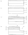
図2を参照に、発光層13のより詳細な構成について説明する。
次に、実施例1の発光素子の製造工程について図3、4を参照に説明する。なお、III 族窒化物半導体の結晶成長には常圧MOCVD法を用いる。MOCVD法において用いる原料ガスは、窒素源として、アンモニア(NH3 )、Ga源として、トリメチルガリウム(TMG;Ga(CH3 )3 )、In源として、トリメチルインジウム(TMI;In(CH3 )3 )、Al源として、トリメチルアルミニウム(TMA;Al(CH3 )3 )、n型ドーピングガスとして、シラン(SiH4 )、p型ドーピングガスとしてビスシクロペンタジエニルマグネシウム(Cp2 Mg;Mg(C2 H5 )2 )、キャリアガスとして水素(H2 )、窒素(N2 )である。もちろん、原料ガスとしてこれら以外にも従来MOCVD法によるIII 族窒化物半導体の結晶成長に用いられている材料を使用することができる。たとえば、In原料ガスとして、TMI意外にトリエチルインジウム(TEI;In(C2 H5 )3 )なども用いることができる。
次に、実施例1の発光素子についての各種実験結果を説明する。
実施例1では、発光層13の第1保護層13Bについて、In原料ガスをパルス供給してIn組成比が0%より大きく3%以下のInGaNからなる第1保護層13Bを形成しているが、本発明はこれに限るものではない。本発明は、低温でInを含むIII 族窒化物半導体(InGaN、AlGaInN、AlInNなど)を形成する場合であれば適用できる。たとえば、発光素子の他の構成部分に本発明を適用してもよいし、発光素子以外の半導体素子に本発明を適用してもよい。
11:nコンタクト層
12:nクラッド層
13:発光層
13A:井戸層
13B:第1保護層
13C:第2保護層
13D:障壁層
14:pクラッド層
15:pコンタクト層
16:透明電極
17:p電極
18:n電極
Claims (8)
- MQW構造の発光層を有するIII 族窒化物半導体からなる発光素子の製造方法において、
前記発光層は、MOCVD法により、Inを含むIII 族窒化物半導体からなる井戸層、前記井戸層以上のバンドギャップであるInを含むIII 族窒化物半導体からなる第1保護層、Alを含むIII 族窒化物半導体からなり、前記第1保護層よりもバンドギャップが大きくなるようにAl組成比が設定された第2保護層、前記井戸層よりも大きなバンドギャップであるIII 族窒化物半導体からなる障壁層とを順に繰り返し積層することにより形成し、
前記第1保護層は、前記井戸層と同一温度で形成し、In原料ガスをパルス供給して形成することで、In組成を0%より大きく3%以下とした、
ことを特徴とする発光素子の製造方法。 - In原料ガスをパルス供給する際のデューティー比によって、前記第1保護層のIn組成比を制御する、
ことを特徴とする請求項1に記載の発光素子の製造方法。 - In原料ガスをパルス供給する際のパルスのデューティー比は、0より大きく0.95以下とする、ことを特徴とする請求項2に記載の発光素子の製造方法。
- In原料ガスの供給量は、0より大きく2μmol/min以下であることを特徴とする請求項1ないし請求項3のいずれか1項に記載の発光素子の製造方法。
- 前記井戸層および前記第1保護層の成長温度は、700〜850℃とすることを特徴とする請求項1ないし請求項4のいずれか1項に記載の発光素子の製造方法。
- 前記第1保護層は、InGaNであることを特徴とする請求項1ないし請求項5のいずれか1項に記載の発光素子の製造方法。
- 前記第2保護層は、AlGaNであることを特徴とする請求項1ないし請求項6のいずれか1項に記載の発光素子の製造方法。
- In原料ガスはトリメチルインジウムであることを特徴とする請求項1ないし請求項7に記載の発光素子の製造方法。
Priority Applications (3)
| Application Number | Priority Date | Filing Date | Title |
|---|---|---|---|
| JP2014223861A JP6281469B2 (ja) | 2014-11-03 | 2014-11-03 | 発光素子の製造方法 |
| CN201510729034.9A CN105576085B (zh) | 2014-11-03 | 2015-10-30 | 制造发光器件的方法及制造第iii族氮化物半导体的方法 |
| US14/928,904 US9595633B2 (en) | 2014-11-03 | 2015-10-30 | Method for producing light-emitting device and method for producing group III nitride semiconductor |
Applications Claiming Priority (1)
| Application Number | Priority Date | Filing Date | Title |
|---|---|---|---|
| JP2014223861A JP6281469B2 (ja) | 2014-11-03 | 2014-11-03 | 発光素子の製造方法 |
Publications (2)
| Publication Number | Publication Date |
|---|---|
| JP2016092162A JP2016092162A (ja) | 2016-05-23 |
| JP6281469B2 true JP6281469B2 (ja) | 2018-02-21 |
Family
ID=55853606
Family Applications (1)
| Application Number | Title | Priority Date | Filing Date |
|---|---|---|---|
| JP2014223861A Active JP6281469B2 (ja) | 2014-11-03 | 2014-11-03 | 発光素子の製造方法 |
Country Status (3)
| Country | Link |
|---|---|
| US (1) | US9595633B2 (ja) |
| JP (1) | JP6281469B2 (ja) |
| CN (1) | CN105576085B (ja) |
Families Citing this family (1)
| Publication number | Priority date | Publication date | Assignee | Title |
|---|---|---|---|---|
| CN108346722B (zh) * | 2017-01-19 | 2019-09-06 | 厦门乾照光电股份有限公司 | 一种蓝绿发光二极管及其外延方法 |
Family Cites Families (17)
| Publication number | Priority date | Publication date | Assignee | Title |
|---|---|---|---|---|
| JP3304782B2 (ja) * | 1996-09-08 | 2002-07-22 | 豊田合成株式会社 | 半導体発光素子 |
| JP3624794B2 (ja) | 2000-05-24 | 2005-03-02 | 豊田合成株式会社 | Iii族窒化物系化合物半導体発光素子の製造方法 |
| JP2003304034A (ja) * | 2002-04-12 | 2003-10-24 | Sony Corp | 半導体素子の製造方法 |
| JP4285949B2 (ja) * | 2002-06-27 | 2009-06-24 | シャープ株式会社 | 窒化物半導体発光素子 |
| KR100482511B1 (ko) * | 2004-02-05 | 2005-04-14 | 에피밸리 주식회사 | Ⅲ-질화물계 반도체 발광소자 |
| JP4389723B2 (ja) * | 2004-02-17 | 2009-12-24 | 住友電気工業株式会社 | 半導体素子を形成する方法 |
| JP2006156891A (ja) * | 2004-12-01 | 2006-06-15 | Sharp Corp | 窒化物半導体発光素子および窒化物半導体発光素子の製造方法 |
| JP2007305909A (ja) * | 2006-05-15 | 2007-11-22 | Kyocera Corp | 窒化ガリウム系化合物半導体の製造方法及び発光素子の製造方法 |
| JP4668225B2 (ja) * | 2007-03-27 | 2011-04-13 | シャープ株式会社 | 窒化物半導体発光素子の製造方法 |
| EP2325899A4 (en) * | 2008-08-29 | 2015-04-29 | Toshiba Kk | SEMICONDUCTOR COMPONENT |
| JP5332451B2 (ja) * | 2008-09-25 | 2013-11-06 | 豊田合成株式会社 | Iii族窒化物系化合物半導体発光素子及びその製造方法 |
| JP5737111B2 (ja) | 2011-03-30 | 2015-06-17 | 豊田合成株式会社 | Iii族窒化物半導体発光素子 |
| JP2013214700A (ja) * | 2012-03-07 | 2013-10-17 | Toshiba Corp | 半導体発光素子 |
| US9312432B2 (en) * | 2012-03-13 | 2016-04-12 | Tsmc Solid State Lighting Ltd. | Growing an improved P-GaN layer of an LED through pressure ramping |
| CN203192830U (zh) * | 2013-03-13 | 2013-09-11 | 扬州中科半导体照明有限公司 | 高亮度GaN基绿光LED的MQW结构 |
| CN103258927A (zh) * | 2013-05-16 | 2013-08-21 | 合肥彩虹蓝光科技有限公司 | 一种提高GaN基LED抗静电能力的外延结构及其生长方法 |
| US9443963B2 (en) * | 2014-04-07 | 2016-09-13 | International Business Machines Corporation | SiGe FinFET with improved junction doping control |
-
2014
- 2014-11-03 JP JP2014223861A patent/JP6281469B2/ja active Active
-
2015
- 2015-10-30 US US14/928,904 patent/US9595633B2/en not_active Expired - Fee Related
- 2015-10-30 CN CN201510729034.9A patent/CN105576085B/zh active Active
Also Published As
| Publication number | Publication date |
|---|---|
| US20160126415A1 (en) | 2016-05-05 |
| US9595633B2 (en) | 2017-03-14 |
| CN105576085B (zh) | 2019-03-12 |
| CN105576085A (zh) | 2016-05-11 |
| JP2016092162A (ja) | 2016-05-23 |
Similar Documents
| Publication | Publication Date | Title |
|---|---|---|
| JP5634368B2 (ja) | 半導体装置 | |
| JP5533744B2 (ja) | Iii族窒化物半導体発光素子 | |
| CN104919604B (zh) | 氮化物半导体发光元件 | |
| KR101399250B1 (ko) | 질소 화합물 반도체 발광 소자 및 그 제조 방법 | |
| US8980657B2 (en) | Method for producing a group III nitride semiconductor light-emitting device | |
| JP2012169383A (ja) | Iii族窒化物半導体発光素子およびその製造方法 | |
| JP2014187159A (ja) | 半導体発光素子 | |
| CN102810607B (zh) | 用于制造iii族氮化物半导体发光器件的方法 | |
| US9391237B2 (en) | Method for producing group III nitride semiconductor light-emitting device | |
| JP5874592B2 (ja) | Iii族窒化物半導体発光素子の製造方法 | |
| JP5423026B2 (ja) | Iii族窒化物半導体発光素子およびその製造方法 | |
| JP4457691B2 (ja) | GaN系半導体素子の製造方法 | |
| US9564552B2 (en) | Method for producing group III nitride semiconductor light-emitting device | |
| JP6281469B2 (ja) | 発光素子の製造方法 | |
| TWI360234B (en) | Production method of group iii nitride semiconduct | |
| JP2006210692A (ja) | 3族窒化物系化合物半導体発光素子 | |
| JP2008118048A (ja) | GaN系半導体発光素子 | |
| US9508895B2 (en) | Group III nitride semiconductor light-emitting device and production method therefor | |
| JP6478685B2 (ja) | 半導体発光素子 | |
| JP2009272316A (ja) | 窒化物系半導体素子及びその製造方法 | |
| JP2018014517A (ja) | 半導体発光素子 | |
| JP2009177219A (ja) | GaN系半導体素子の製造方法 |
Legal Events
| Date | Code | Title | Description |
|---|---|---|---|
| A621 | Written request for application examination |
Free format text: JAPANESE INTERMEDIATE CODE: A621 Effective date: 20161219 |
|
| A977 | Report on retrieval |
Free format text: JAPANESE INTERMEDIATE CODE: A971007 Effective date: 20171018 |
|
| A131 | Notification of reasons for refusal |
Free format text: JAPANESE INTERMEDIATE CODE: A131 Effective date: 20171024 |
|
| A521 | Request for written amendment filed |
Free format text: JAPANESE INTERMEDIATE CODE: A523 Effective date: 20171115 |
|
| TRDD | Decision of grant or rejection written | ||
| A01 | Written decision to grant a patent or to grant a registration (utility model) |
Free format text: JAPANESE INTERMEDIATE CODE: A01 Effective date: 20171226 |
|
| A61 | First payment of annual fees (during grant procedure) |
Free format text: JAPANESE INTERMEDIATE CODE: A61 Effective date: 20180108 |
|
| R150 | Certificate of patent or registration of utility model |
Ref document number: 6281469 Country of ref document: JP Free format text: JAPANESE INTERMEDIATE CODE: R150 |