JP6282979B2 - プラズマ処理装置 - Google Patents
プラズマ処理装置 Download PDFInfo
- Publication number
- JP6282979B2 JP6282979B2 JP2014543186A JP2014543186A JP6282979B2 JP 6282979 B2 JP6282979 B2 JP 6282979B2 JP 2014543186 A JP2014543186 A JP 2014543186A JP 2014543186 A JP2014543186 A JP 2014543186A JP 6282979 B2 JP6282979 B2 JP 6282979B2
- Authority
- JP
- Japan
- Prior art keywords
- electrode
- plasma
- substrate
- process gas
- electrodes
- Prior art date
- Legal status (The legal status is an assumption and is not a legal conclusion. Google has not performed a legal analysis and makes no representation as to the accuracy of the status listed.)
- Active
Links
Images




Classifications
-
- H—ELECTRICITY
- H01—ELECTRIC ELEMENTS
- H01J—ELECTRIC DISCHARGE TUBES OR DISCHARGE LAMPS
- H01J37/00—Discharge tubes with provision for introducing objects or material to be exposed to the discharge, e.g. for the purpose of examination or processing thereof
- H01J37/32—Gas-filled discharge tubes
- H01J37/32431—Constructional details of the reactor
- H01J37/32532—Electrodes
-
- H—ELECTRICITY
- H01—ELECTRIC ELEMENTS
- H01J—ELECTRIC DISCHARGE TUBES OR DISCHARGE LAMPS
- H01J37/00—Discharge tubes with provision for introducing objects or material to be exposed to the discharge, e.g. for the purpose of examination or processing thereof
- H01J37/32—Gas-filled discharge tubes
- H01J37/32009—Arrangements for generation of plasma specially adapted for examination or treatment of objects, e.g. plasma sources
- H01J37/32018—Glow discharge
- H01J37/32036—AC powered
-
- H—ELECTRICITY
- H01—ELECTRIC ELEMENTS
- H01J—ELECTRIC DISCHARGE TUBES OR DISCHARGE LAMPS
- H01J37/00—Discharge tubes with provision for introducing objects or material to be exposed to the discharge, e.g. for the purpose of examination or processing thereof
- H01J37/32—Gas-filled discharge tubes
- H01J37/32009—Arrangements for generation of plasma specially adapted for examination or treatment of objects, e.g. plasma sources
- H01J37/32082—Radio frequency generated discharge
- H01J37/32091—Radio frequency generated discharge the radio frequency energy being capacitively coupled to the plasma
-
- H—ELECTRICITY
- H01—ELECTRIC ELEMENTS
- H01J—ELECTRIC DISCHARGE TUBES OR DISCHARGE LAMPS
- H01J37/00—Discharge tubes with provision for introducing objects or material to be exposed to the discharge, e.g. for the purpose of examination or processing thereof
- H01J37/32—Gas-filled discharge tubes
- H01J37/32431—Constructional details of the reactor
- H01J37/3244—Gas supply means
-
- H—ELECTRICITY
- H01—ELECTRIC ELEMENTS
- H01J—ELECTRIC DISCHARGE TUBES OR DISCHARGE LAMPS
- H01J37/00—Discharge tubes with provision for introducing objects or material to be exposed to the discharge, e.g. for the purpose of examination or processing thereof
- H01J37/32—Gas-filled discharge tubes
- H01J37/32431—Constructional details of the reactor
- H01J37/32532—Electrodes
- H01J37/32541—Shape
-
- H—ELECTRICITY
- H01—ELECTRIC ELEMENTS
- H01J—ELECTRIC DISCHARGE TUBES OR DISCHARGE LAMPS
- H01J37/00—Discharge tubes with provision for introducing objects or material to be exposed to the discharge, e.g. for the purpose of examination or processing thereof
- H01J37/32—Gas-filled discharge tubes
- H01J37/32431—Constructional details of the reactor
- H01J37/32532—Electrodes
- H01J37/32568—Relative arrangement or disposition of electrodes; moving means
Landscapes
- Engineering & Computer Science (AREA)
- Physics & Mathematics (AREA)
- Plasma & Fusion (AREA)
- Chemical & Material Sciences (AREA)
- Analytical Chemistry (AREA)
- Power Engineering (AREA)
- Plasma Technology (AREA)
- Drying Of Semiconductors (AREA)
- Cleaning Or Drying Semiconductors (AREA)
Description
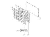
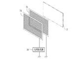
11 基板
14 処理室
18 高周波電源
21 電極ユニット
24 導入口
25,26 電極
31,32 電極セット
31a,31b,32a,32b 電極部
78,79 流路制御板
Claims (2)
- 被処理物を処理室内に収容し、真空にした処理室内に導入したプロセスガスからプラズマを発生させ、このプラズマによって被処理物に処理を行うプラズマ処理装置において、
プラズマ発生用の高周波電圧を出力する電源と、
複数の棒状の電極を所定の間隔で互いに平行に配列した第1の電極部、及び前記第1の電極部と離間して配され、複数の棒状の電極を所定の間隔で互いに平行に配列した第2の電極部を有し、前記電源からの高周波電圧によってプロセスガスを励起させてプラズマを発生させる一対の電極セットと、前記一対の電極セットの間で被処理物の表面を露呈させて保持するホルダーとを有し、前記第1及び第2の電極部の各電極は被処理物の表面に平行に配される電極ユニットと、
プロセスガスを処理室内に導入する複数の導入口を有し、前記複数の導入口から前記電極ユニットに向けて、前記第1及び第2の電極部における電極の並ぶ方向にプロセスガスを放出し、プロセスガスを被処理物の表面に平行に流すガス導入部と、
被処理物を挟んで前記導入口と対向する位置に設けられ、処理室内の排気を行う排気口と、
前記ガス導入部から放出されたプロセスガスが前記電極ユニットと処理室との間を通って前記排気口側に流れることを制限する流路制御部材と
を備えるプラズマ処理装置。 - 前記導入口は、前記ガス導入部の前記電極ユニットに対応する面の領域に均一に分布する請求項1記載のプラズマ処理装置。
Applications Claiming Priority (3)
| Application Number | Priority Date | Filing Date | Title |
|---|---|---|---|
| JPPCT/JP2012/077454 | 2012-10-24 | ||
| PCT/JP2012/077454 WO2014064779A1 (ja) | 2012-10-24 | 2012-10-24 | プラズマ処理装置及び方法 |
| PCT/JP2013/074607 WO2014065034A1 (ja) | 2012-10-24 | 2013-09-12 | プラズマ処理装置及び方法 |
Publications (2)
| Publication Number | Publication Date |
|---|---|
| JPWO2014065034A1 JPWO2014065034A1 (ja) | 2016-09-08 |
| JP6282979B2 true JP6282979B2 (ja) | 2018-02-21 |
Family
ID=50544177
Family Applications (1)
| Application Number | Title | Priority Date | Filing Date |
|---|---|---|---|
| JP2014543186A Active JP6282979B2 (ja) | 2012-10-24 | 2013-09-12 | プラズマ処理装置 |
Country Status (5)
| Country | Link |
|---|---|
| US (1) | US20150228461A1 (ja) |
| JP (1) | JP6282979B2 (ja) |
| CN (1) | CN104813746A (ja) |
| TW (1) | TWI631877B (ja) |
| WO (2) | WO2014064779A1 (ja) |
Families Citing this family (14)
| Publication number | Priority date | Publication date | Assignee | Title |
|---|---|---|---|---|
| US8372238B2 (en) * | 2008-05-20 | 2013-02-12 | Nordson Corporation | Multiple-electrode plasma processing systems with confined process chambers and interior-bussed electrical connections with the electrodes |
| JP6385198B2 (ja) * | 2014-08-21 | 2018-09-05 | 日東電工株式会社 | 回路付サスペンション基板の製造方法 |
| DE112017001370T5 (de) * | 2016-03-17 | 2018-11-29 | Jcu Corporation | Plasmaerzeugungsvorrichtung |
| CN108885983B (zh) | 2016-05-30 | 2022-11-11 | 株式会社Jcu | 等离子处理装置及方法 |
| JP6652644B2 (ja) * | 2016-07-21 | 2020-02-26 | 株式会社Kokusai Electric | プラズマ生成装置、基板処理装置、半導体装置の製造方法及びプログラム |
| US10851457B2 (en) | 2017-08-31 | 2020-12-01 | Lam Research Corporation | PECVD deposition system for deposition on selective side of the substrate |
| US20190157048A1 (en) * | 2017-11-17 | 2019-05-23 | Taiwan Semiconductor Manufacturing Co., Ltd. | Plasma processing apparatus and method for forming semiconductor device structure |
| CN110402007B (zh) * | 2019-07-31 | 2021-10-01 | 北京交通大学 | 一种基于空气辉光放电等离子体的材料表面处理装置 |
| CN121496360A (zh) | 2019-08-16 | 2026-02-10 | 朗姆研究公司 | 空间可调沉积以在晶片差异弯曲中进行补偿 |
| JP7407607B2 (ja) * | 2020-01-31 | 2024-01-04 | 株式会社Screenホールディングス | プラズマ発生装置および基板処理装置 |
| CN111348431B (zh) * | 2020-03-13 | 2022-02-11 | 苏州市奥普斯等离子体科技有限公司 | 一种半离线式等离子体处理设备及其使用方法 |
| CN113518510B (zh) * | 2020-04-10 | 2022-10-11 | 南通深南电路有限公司 | 一种pcb板除胶装置和方法 |
| TWI755292B (zh) * | 2021-02-26 | 2022-02-11 | 友威科技股份有限公司 | 可單面或雙面電漿製程機台 |
| JP7492990B2 (ja) | 2022-06-24 | 2024-05-30 | 株式会社アルバック | プラズマ処理装置およびプラズマ処理方法 |
Family Cites Families (15)
| Publication number | Priority date | Publication date | Assignee | Title |
|---|---|---|---|---|
| GB1582231A (en) * | 1976-08-13 | 1981-01-07 | Nat Res Dev | Application of a layer of carbonaceous material to a surface |
| JP3117366B2 (ja) * | 1994-07-25 | 2000-12-11 | 三菱重工業株式会社 | プラズマ処理装置 |
| JP2000269196A (ja) * | 1999-03-19 | 2000-09-29 | Toshiba Corp | プラズマ処理方法及びプラズマ処理装置 |
| JP3842935B2 (ja) * | 1999-10-22 | 2006-11-08 | 三菱重工業株式会社 | トレイレス斜め基板搬送装置 |
| JP4161533B2 (ja) * | 2000-12-28 | 2008-10-08 | 松下電工株式会社 | プラズマ処理方法及びプラズマ処理装置 |
| JP4770029B2 (ja) * | 2001-01-22 | 2011-09-07 | 株式会社Ihi | プラズマcvd装置及び太陽電池の製造方法 |
| US6852169B2 (en) * | 2001-05-16 | 2005-02-08 | Nordson Corporation | Apparatus and methods for processing optical fibers with a plasma |
| US6820570B2 (en) * | 2001-08-15 | 2004-11-23 | Nobel Biocare Services Ag | Atomic layer deposition reactor |
| US7090705B2 (en) * | 2002-10-16 | 2006-08-15 | Sharp Kabushiki Kaisha | Electronic device, production method thereof, and plasma process apparatus |
| JP4426783B2 (ja) * | 2003-06-27 | 2010-03-03 | 積水化学工業株式会社 | プラズマ処理装置及び処理方法 |
| US7594977B2 (en) * | 2004-05-25 | 2009-09-29 | Tsubaki Seiko, Inc | Tape bonder, tape bonding method, and process for manufacturing electronic component |
| US20050067934A1 (en) * | 2003-09-26 | 2005-03-31 | Ishikawajima-Harima Heavy Industries Co., Ltd. | Discharge apparatus, plasma processing method and solar cell |
| JP4549735B2 (ja) * | 2004-05-21 | 2010-09-22 | フィーサ株式会社 | プラズマ処理方法及び装置 |
| JP5031252B2 (ja) * | 2006-03-30 | 2012-09-19 | 東京エレクトロン株式会社 | プラズマ処理装置 |
| US20090165714A1 (en) * | 2008-01-01 | 2009-07-02 | Dongguan Anwell Digital Machinery Ltd. | Method and system for processing substrates in chambers |
-
2012
- 2012-10-24 WO PCT/JP2012/077454 patent/WO2014064779A1/ja not_active Ceased
-
2013
- 2013-09-12 CN CN201380055979.6A patent/CN104813746A/zh active Pending
- 2013-09-12 WO PCT/JP2013/074607 patent/WO2014065034A1/ja not_active Ceased
- 2013-09-12 JP JP2014543186A patent/JP6282979B2/ja active Active
- 2013-10-01 TW TW102135547A patent/TWI631877B/zh active
-
2015
- 2015-04-21 US US14/691,776 patent/US20150228461A1/en not_active Abandoned
Also Published As
| Publication number | Publication date |
|---|---|
| WO2014064779A1 (ja) | 2014-05-01 |
| TW201431444A (zh) | 2014-08-01 |
| WO2014065034A1 (ja) | 2014-05-01 |
| US20150228461A1 (en) | 2015-08-13 |
| JPWO2014065034A1 (ja) | 2016-09-08 |
| TWI631877B (zh) | 2018-08-01 |
| CN104813746A (zh) | 2015-07-29 |
Similar Documents
| Publication | Publication Date | Title |
|---|---|---|
| JPWO2014065034A1 (ja) | プラズマ処理装置及び方法 | |
| KR102582878B1 (ko) | 정전 흡착 방법 및 기판 처리 장치 | |
| JP5248370B2 (ja) | シャワーヘッド及びプラズマ処理装置 | |
| JP2010016021A (ja) | プラズマ処理装置 | |
| US11538664B2 (en) | Plasma treatment apparatus and method | |
| JP6465442B2 (ja) | プラズマ処理装置 | |
| CN101490792B (zh) | 离子沉积设备 | |
| KR20180014656A (ko) | 기판 처리 장치 및 기판 처리 방법 | |
| US20110120495A1 (en) | Plasma processing method | |
| US20140144382A1 (en) | Plasma apparatus | |
| JP5996654B2 (ja) | プラズマ処理装置 | |
| JP5943789B2 (ja) | 大気圧プラズマ成膜装置 | |
| KR101894598B1 (ko) | 플라즈마 처리 장치 | |
| KR102800612B1 (ko) | 기판 처리 장치 및 이를 이용한 기판 처리 방법 | |
| JP2004211161A (ja) | プラズマ発生装置 | |
| KR100683255B1 (ko) | 플라즈마 처리 장치 및 배기 장치 | |
| KR20140009910A (ko) | 전계 압축형 면방전 전극을 포함하는 플라즈마 처리 장치 | |
| JP2004008830A (ja) | プラズマ洗浄装置 | |
| KR20210004741A (ko) | 플라즈마 토치 및 이를 구비하는 반도체 제조 설비의 부품 처리 시스템 | |
| KR101480095B1 (ko) | 원격 플라즈마 처리용 소스 | |
| KR20110027900A (ko) | 플라즈마 발생장치 및 기판 처리장치 | |
| JP5597504B2 (ja) | プラズマ処理装置及び前処理方法 | |
| JP2007237080A (ja) | プラズマ洗浄処理装置 | |
| JPH04364037A (ja) | プラズマ処理装置 | |
| JP2005093705A (ja) | プラズマ生成装置及びプラズマ生成方法 |
Legal Events
| Date | Code | Title | Description |
|---|---|---|---|
| A621 | Written request for application examination |
Free format text: JAPANESE INTERMEDIATE CODE: A621 Effective date: 20160823 |
|
| A131 | Notification of reasons for refusal |
Free format text: JAPANESE INTERMEDIATE CODE: A131 Effective date: 20170705 |
|
| A521 | Request for written amendment filed |
Free format text: JAPANESE INTERMEDIATE CODE: A523 Effective date: 20170829 |
|
| TRDD | Decision of grant or rejection written | ||
| A01 | Written decision to grant a patent or to grant a registration (utility model) |
Free format text: JAPANESE INTERMEDIATE CODE: A01 Effective date: 20180110 |
|
| A61 | First payment of annual fees (during grant procedure) |
Free format text: JAPANESE INTERMEDIATE CODE: A61 Effective date: 20180125 |
|
| R150 | Certificate of patent or registration of utility model |
Ref document number: 6282979 Country of ref document: JP Free format text: JAPANESE INTERMEDIATE CODE: R150 |
|
| R250 | Receipt of annual fees |
Free format text: JAPANESE INTERMEDIATE CODE: R250 |
|
| R250 | Receipt of annual fees |
Free format text: JAPANESE INTERMEDIATE CODE: R250 |
|
| R250 | Receipt of annual fees |
Free format text: JAPANESE INTERMEDIATE CODE: R250 |
|
| R250 | Receipt of annual fees |
Free format text: JAPANESE INTERMEDIATE CODE: R250 |
|
| R250 | Receipt of annual fees |
Free format text: JAPANESE INTERMEDIATE CODE: R250 |
|
| R250 | Receipt of annual fees |
Free format text: JAPANESE INTERMEDIATE CODE: R250 |