JP6288038B2 - 発光装置、光書込み装置及び画像形成装置 - Google Patents
発光装置、光書込み装置及び画像形成装置 Download PDFInfo
- Publication number
- JP6288038B2 JP6288038B2 JP2015210435A JP2015210435A JP6288038B2 JP 6288038 B2 JP6288038 B2 JP 6288038B2 JP 2015210435 A JP2015210435 A JP 2015210435A JP 2015210435 A JP2015210435 A JP 2015210435A JP 6288038 B2 JP6288038 B2 JP 6288038B2
- Authority
- JP
- Japan
- Prior art keywords
- oled
- light
- temperature
- amount
- voltage
- Prior art date
- Legal status (The legal status is an assumption and is not a legal conclusion. Google has not performed a legal analysis and makes no representation as to the accuracy of the status listed.)
- Active
Links
- 230000003287 optical effect Effects 0.000 title claims description 33
- 238000012937 correction Methods 0.000 claims description 58
- 239000010409 thin film Substances 0.000 claims description 17
- 230000001186 cumulative effect Effects 0.000 claims description 13
- 239000000758 substrate Substances 0.000 claims description 11
- 238000001514 detection method Methods 0.000 claims description 3
- 230000007613 environmental effect Effects 0.000 claims description 2
- 238000012546 transfer Methods 0.000 description 14
- 239000003990 capacitor Substances 0.000 description 11
- 230000002093 peripheral effect Effects 0.000 description 10
- 238000007789 sealing Methods 0.000 description 8
- 238000010586 diagram Methods 0.000 description 5
- 238000000034 method Methods 0.000 description 4
- 230000000694 effects Effects 0.000 description 3
- 238000012545 processing Methods 0.000 description 3
- IJGRMHOSHXDMSA-UHFFFAOYSA-N Atomic nitrogen Chemical compound N#N IJGRMHOSHXDMSA-UHFFFAOYSA-N 0.000 description 2
- 238000012986 modification Methods 0.000 description 2
- 230000004048 modification Effects 0.000 description 2
- 241000220317 Rosa Species 0.000 description 1
- 239000003086 colorant Substances 0.000 description 1
- 238000004891 communication Methods 0.000 description 1
- 238000007796 conventional method Methods 0.000 description 1
- 230000003247 decreasing effect Effects 0.000 description 1
- 229920005994 diacetyl cellulose Polymers 0.000 description 1
- 239000011521 glass Substances 0.000 description 1
- 239000003230 hygroscopic agent Substances 0.000 description 1
- 239000000463 material Substances 0.000 description 1
- 229910052757 nitrogen Inorganic materials 0.000 description 1
- 108091008695 photoreceptors Proteins 0.000 description 1
- 238000005096 rolling process Methods 0.000 description 1
- 229920006395 saturated elastomer Polymers 0.000 description 1
- 239000005394 sealing glass Substances 0.000 description 1
- 239000004065 semiconductor Substances 0.000 description 1
- 125000006850 spacer group Chemical group 0.000 description 1
- 230000002123 temporal effect Effects 0.000 description 1
Images




Classifications
-
- G—PHYSICS
- G09—EDUCATION; CRYPTOGRAPHY; DISPLAY; ADVERTISING; SEALS
- G09G—ARRANGEMENTS OR CIRCUITS FOR CONTROL OF INDICATING DEVICES USING STATIC MEANS TO PRESENT VARIABLE INFORMATION
- G09G3/00—Control arrangements or circuits, of interest only in connection with visual indicators other than cathode-ray tubes
- G09G3/20—Control arrangements or circuits, of interest only in connection with visual indicators other than cathode-ray tubes for presentation of an assembly of a number of characters, e.g. a page, by composing the assembly by combination of individual elements arranged in a matrix no fixed position being assigned to or needed to be assigned to the individual characters or partial characters
- G09G3/22—Control arrangements or circuits, of interest only in connection with visual indicators other than cathode-ray tubes for presentation of an assembly of a number of characters, e.g. a page, by composing the assembly by combination of individual elements arranged in a matrix no fixed position being assigned to or needed to be assigned to the individual characters or partial characters using controlled light sources
- G09G3/30—Control arrangements or circuits, of interest only in connection with visual indicators other than cathode-ray tubes for presentation of an assembly of a number of characters, e.g. a page, by composing the assembly by combination of individual elements arranged in a matrix no fixed position being assigned to or needed to be assigned to the individual characters or partial characters using controlled light sources using electroluminescent panels
- G09G3/32—Control arrangements or circuits, of interest only in connection with visual indicators other than cathode-ray tubes for presentation of an assembly of a number of characters, e.g. a page, by composing the assembly by combination of individual elements arranged in a matrix no fixed position being assigned to or needed to be assigned to the individual characters or partial characters using controlled light sources using electroluminescent panels semiconductive, e.g. using light-emitting diodes [LED]
- G09G3/3208—Control arrangements or circuits, of interest only in connection with visual indicators other than cathode-ray tubes for presentation of an assembly of a number of characters, e.g. a page, by composing the assembly by combination of individual elements arranged in a matrix no fixed position being assigned to or needed to be assigned to the individual characters or partial characters using controlled light sources using electroluminescent panels semiconductive, e.g. using light-emitting diodes [LED] organic, e.g. using organic light-emitting diodes [OLED]
-
- G—PHYSICS
- G03—PHOTOGRAPHY; CINEMATOGRAPHY; ANALOGOUS TECHNIQUES USING WAVES OTHER THAN OPTICAL WAVES; ELECTROGRAPHY; HOLOGRAPHY
- G03G—ELECTROGRAPHY; ELECTROPHOTOGRAPHY; MAGNETOGRAPHY
- G03G15/00—Apparatus for electrographic processes using a charge pattern
- G03G15/04—Apparatus for electrographic processes using a charge pattern for exposing, i.e. imagewise exposure by optically projecting the original image on a photoconductive recording material
- G03G15/04036—Details of illuminating systems, e.g. lamps, reflectors
- G03G15/04045—Details of illuminating systems, e.g. lamps, reflectors for exposing image information provided otherwise than by directly projecting the original image onto the photoconductive recording material, e.g. digital copiers
- G03G15/04054—Details of illuminating systems, e.g. lamps, reflectors for exposing image information provided otherwise than by directly projecting the original image onto the photoconductive recording material, e.g. digital copiers by LED arrays
-
- G—PHYSICS
- G03—PHOTOGRAPHY; CINEMATOGRAPHY; ANALOGOUS TECHNIQUES USING WAVES OTHER THAN OPTICAL WAVES; ELECTROGRAPHY; HOLOGRAPHY
- G03G—ELECTROGRAPHY; ELECTROPHOTOGRAPHY; MAGNETOGRAPHY
- G03G15/00—Apparatus for electrographic processes using a charge pattern
- G03G15/04—Apparatus for electrographic processes using a charge pattern for exposing, i.e. imagewise exposure by optically projecting the original image on a photoconductive recording material
- G03G15/04036—Details of illuminating systems, e.g. lamps, reflectors
- G03G15/04045—Details of illuminating systems, e.g. lamps, reflectors for exposing image information provided otherwise than by directly projecting the original image onto the photoconductive recording material, e.g. digital copiers
- G03G15/04063—Details of illuminating systems, e.g. lamps, reflectors for exposing image information provided otherwise than by directly projecting the original image onto the photoconductive recording material, e.g. digital copiers by EL-bars
-
- G—PHYSICS
- G03—PHOTOGRAPHY; CINEMATOGRAPHY; ANALOGOUS TECHNIQUES USING WAVES OTHER THAN OPTICAL WAVES; ELECTROGRAPHY; HOLOGRAPHY
- G03G—ELECTROGRAPHY; ELECTROPHOTOGRAPHY; MAGNETOGRAPHY
- G03G15/00—Apparatus for electrographic processes using a charge pattern
- G03G15/50—Machine control of apparatus for electrographic processes using a charge pattern, e.g. regulating differents parts of the machine, multimode copiers, microprocessor control
-
- G—PHYSICS
- G09—EDUCATION; CRYPTOGRAPHY; DISPLAY; ADVERTISING; SEALS
- G09G—ARRANGEMENTS OR CIRCUITS FOR CONTROL OF INDICATING DEVICES USING STATIC MEANS TO PRESENT VARIABLE INFORMATION
- G09G3/00—Control arrangements or circuits, of interest only in connection with visual indicators other than cathode-ray tubes
- G09G3/20—Control arrangements or circuits, of interest only in connection with visual indicators other than cathode-ray tubes for presentation of an assembly of a number of characters, e.g. a page, by composing the assembly by combination of individual elements arranged in a matrix no fixed position being assigned to or needed to be assigned to the individual characters or partial characters
- G09G3/22—Control arrangements or circuits, of interest only in connection with visual indicators other than cathode-ray tubes for presentation of an assembly of a number of characters, e.g. a page, by composing the assembly by combination of individual elements arranged in a matrix no fixed position being assigned to or needed to be assigned to the individual characters or partial characters using controlled light sources
- G09G3/30—Control arrangements or circuits, of interest only in connection with visual indicators other than cathode-ray tubes for presentation of an assembly of a number of characters, e.g. a page, by composing the assembly by combination of individual elements arranged in a matrix no fixed position being assigned to or needed to be assigned to the individual characters or partial characters using controlled light sources using electroluminescent panels
- G09G3/32—Control arrangements or circuits, of interest only in connection with visual indicators other than cathode-ray tubes for presentation of an assembly of a number of characters, e.g. a page, by composing the assembly by combination of individual elements arranged in a matrix no fixed position being assigned to or needed to be assigned to the individual characters or partial characters using controlled light sources using electroluminescent panels semiconductive, e.g. using light-emitting diodes [LED]
- G09G3/3208—Control arrangements or circuits, of interest only in connection with visual indicators other than cathode-ray tubes for presentation of an assembly of a number of characters, e.g. a page, by composing the assembly by combination of individual elements arranged in a matrix no fixed position being assigned to or needed to be assigned to the individual characters or partial characters using controlled light sources using electroluminescent panels semiconductive, e.g. using light-emitting diodes [LED] organic, e.g. using organic light-emitting diodes [OLED]
- G09G3/3225—Control arrangements or circuits, of interest only in connection with visual indicators other than cathode-ray tubes for presentation of an assembly of a number of characters, e.g. a page, by composing the assembly by combination of individual elements arranged in a matrix no fixed position being assigned to or needed to be assigned to the individual characters or partial characters using controlled light sources using electroluminescent panels semiconductive, e.g. using light-emitting diodes [LED] organic, e.g. using organic light-emitting diodes [OLED] using an active matrix
- G09G3/3233—Control arrangements or circuits, of interest only in connection with visual indicators other than cathode-ray tubes for presentation of an assembly of a number of characters, e.g. a page, by composing the assembly by combination of individual elements arranged in a matrix no fixed position being assigned to or needed to be assigned to the individual characters or partial characters using controlled light sources using electroluminescent panels semiconductive, e.g. using light-emitting diodes [LED] organic, e.g. using organic light-emitting diodes [OLED] using an active matrix with pixel circuitry controlling the current through the light-emitting element
Landscapes
- Physics & Mathematics (AREA)
- General Physics & Mathematics (AREA)
- Engineering & Computer Science (AREA)
- Computer Hardware Design (AREA)
- Theoretical Computer Science (AREA)
- Printers Or Recording Devices Using Electromagnetic And Radiation Means (AREA)
- Electroluminescent Light Sources (AREA)
- Microelectronics & Electronic Packaging (AREA)
- Facsimile Heads (AREA)
Description
このような光書込み装置(OLED-PH: OLED Print Head)は、主走査方向に多数(例えば、15,000個)配列した発光素子を点灯することによって光書込みを行うため、発光素子間で光量にムラがあると静電潜像、延いてはトナー像において主走査方向における濃度ムラが発生して、優れた画質を達成することができなくなる。
TFT02の閾値電圧Vthには初期バラつきがあり、更に、TFT1402のドレイン電流Idは閾値電圧Vthと略比例の関係にある。このため、TFT02に同じ電圧Vdgを印加しても供給される駆動電流Idがバラついて、発光素子1401の光量が一定しなくなる。
また、別の従来技術においては、予めすべての発光素子を同一条件で発光させて発光素子毎の光量を記憶しておき、記憶しておいた光量に応じて発光素子毎に駆動条件を補正する(特許文献2を参照)。このようにすれば、発光素子の発光効率αにバラつきがあっても、同一条件で発行させた場合に光量が多い発光素子の駆動電流を少なく、光量が少ない発光素子は駆動電流を多くする等、駆動条件を補正するので、光量バラつきを抑えることできる。
OLEDの順方向電圧Velには初期バラつきがあるので、図14に示されるように、発光素子1401とTFT1402との直列回路に印加する電圧Vddが同じであっても、TFT1402に印加されるソース−ドレイン電圧Vsdは、
Vsd = Vdd − Vel
となり、バラついてしまう。
また、前記因子である前記OLEDの温度を指標する指数を取得する温度検出手段と、前記因子である前記OLED毎の累積発光時間を計時する計時手段と、を備え、前記順方向電圧推定手段は、当該OLEDの累積発光時間、温度及び前記設定光量の少なくともひとつに応じて、当該OLEDの順方向電圧を推定してもよい。
更に、前記順方向電圧推定手段は、前記OLEDの累積発光時間、温度及び前記設定光量の少なくともひとつに応じて前記補正係数を推定するためのLUT又は関数を記憶しており、当該LUT又は関数を用いて前記補正係数を推定してもよい。
また、前記駆動電流量推定手段は、前記OLEDの駆動電流量を、当該OLEDの累積発光時間、温度及び前記設定光量の少なくともひとつに応じて推定してもよい。
更に、前記駆動電流量推定手段は、前記OLEDの累積発光時間、温度及び前記設定光量の少なくともひとつに応じて前記補正係数を推定するためのLUT又は関数を記憶しており、当該LUT又は関数を用いて前記補正係数を推定してもよい。
また、本発明に係る光書込み装置は、感光体を露光して光書込みを行う光書込み装置であって、本発明に係る発光装置を複数と、前記OLEDの出射光を前記感光体上に集光する集光手段と、を備え、前記OLEDがライン状に配置されていることを特徴とする。
[1]画像形成装置の構成
まず、本実施の形態に係る画像形成装置の構成について説明する。
図1に示されるように、画像形成装置1は、所謂タンデム型のカラープリンターである。画像形成装置1が備える作像部101Y、101M、101C及び101Kは、制御部102の制御の下、Y(イエロー)、M(マゼンタ)、C(シアン)、K(ブラック)各色のトナー像を形成する。
記録シートSが厚紙である場合には普通紙である場合よりもトナー像を定着するための熱量が多く必要になる。このため、画像形成装置1は、記録シートSの紙種に応じて記録シートSの搬送速度(システム速度)を切り替えて、普通紙の場合には全速搬送し、厚紙の場合には半速搬送する。システム速度に応じて、感光体ドラム110の回転速度も切り替わるので、1画素あたりの露光時間に長短が生じる。
次に、光書込み装置100の構成について説明する。
図2に示されるように、光書込み装置100は、OLEDパネル200とロッドレンズアレイ(SLA: Selfoc Lens Array)202をホルダー203に収容したものであって、OLEDパネル200にはOLED201が実装されている。OLED201が出射した光ビームLは、ロッドレンズアレイ202によって感光体ドラム110の外周面上に集光される。なお、SLAに代えてMLA(Micro Lens Array)を用いてもよい。また、画像形成装置1の必要箇所と接続するためのケーブル等は図示を省略した。
図3に示されるように、OLEDパネル200は、TFT基板300、封止板301及びドライバーIC(Integrated Circuit)302等を備えている。TFT基板300には、15,000個のOLED201が主走査方向に沿ってライン状に配列されている。これらのOLED201は、感光体ドラム110の外周面上で集光点が21.2μmピッチ(1200dpi)になっていれば、一列に配列してもよいし、千鳥配置してもよい。
ドライバーIC302はデジタル輝度信号をアナログ輝度信号(以下、単に「輝度信号」という。)に変換してOLED201毎の駆動回路に入力する。駆動回路は輝度信号に応じてOLED201の駆動電流を生成する。輝度信号は、電流信号であってもよいし電圧信号であってもよい。また、ドライバーIC302には温度センサー320が内蔵されている。ドライバーIC302はOLED201と同じくTFT基板300に実装されているので、温度センサー320で検出された温度Tは、OLED201自体の温度と概ね等しくなっている。
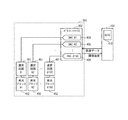
DAC400から発光ブロックに向かう回路上には何れも選択回路401が配設されている。各DAC400は、配下の100個のOLED201に対して、所謂ローリング駆動によって順次、輝度信号を出力する。
シフトレジスター511が選択TFT512をオンした状態で、DAC400の出力電圧がキャパシター521の第1の端子に印加され、保持される。キャパシター521の第1の端子は、駆動TFT522のゲート端子にも接続されており、キャパシター521の第2の端子は駆動TFT522のソース端子並びに電源配線531に接続されている。
定電圧源Vpwrは、OLED201に供給される駆動電流の供給源となっており、駆動TFT522は、キャパシター521の第1、第2の端子間に保持される電圧に応じたドレイン電流を駆動電流としてOLED201に供給する。例えば、キャパシター521にHに相当する信号が書き込まれると、駆動TFT522がオンして、OLED201が発光する。また、キャパシター521にLに相当する信号が書き込まれると、駆動TFT522はオフして、OLED201は発光しない。
[3]ASIC410の構成
まず、ASIC410の構成について説明する。
駆動電流補正部600には設定光量テーブル、初期Velテーブル、Vel補正係数テーブル、初期Idテーブル、Id補正係数テーブル及びTFT特性テーブルという6つのLUT(Look Up Table)が記憶されている。
設定光量テーブルは、図7に示されるように、15,000個あるOLED201のそれぞれについてシステム速度毎に設定光量Lを記録したテーブルである。
設定光量Lは、OLED201が出射すべき光量として予め設定されている光量である。OLED201は、ロッドレンズアレイ202との位置関係によって集光率が異なるため、感光体ドラム110の外周面上での露光量を揃えるために、OLED201毎に光量を調整する必要がある。このため、集光率が高いOLED201の設定光量Lは少なく、集光率が低いOLED201の設定光量Lは多く設定される。
この露光時間の長短に関わらず、1画素あたりの露光量を揃えるためにも、OLED201毎の設定光量が調整される。すなわち、露光時間が長い場合の設定光量は少なく、露光時間が低い場合の設定光量は多くなるように設定される。
図7においては、システム速度が全速時の設定光量Lと半速時の設定光量LとがOLED201毎に記憶される。なお、システム速度は全半速の2種類に限定されないのはいうまでもなく3種類以上であってもよい。
初期Velテーブルは、15,000個あるOLED201のそれぞれについて順方向電圧Velの初期値を設定光量Lごとに記憶するテーブルである。図8(a)に例示する初期Velテーブルにおいては、AからDまでの4種類の設定光量Lのそれぞれについて、各OLED201の順方向電圧Velの初期値が記憶される。なお、設定光量Lが4種類に限定されないのは言うまでもなく、3種類以下或いは5種類以上であってもよい。
Vel補正係数テーブルは、温度範囲ごとに設けられたテーブル群であって、各テーブルはOLED201の設定光量と累積発光時間Eの範囲との組み合わせ毎に順方向電圧Velの補正係数(以下、「Vel補正係数」という。)が記憶されている。図8(b)に例示するVel補正係数テーブルは、摂氏0度から摂氏80度までを10度ずつ8つに分けた温度範囲ごとに設けられている。
(3−4)初期Idテーブル
初期Idテーブルは、15,000個あるOLED201のそれぞれについて駆動電流Idの初期値を設定光量ごとに記憶するテーブルである。図9(a)に例示する初期Idテーブルにおいては、AからDまでの4種類の設定光量のそれぞれについて、15,000個のOLED201毎に駆動電流Idの初期値が記憶される。
Id補正係数テーブルは、温度範囲ごとに設けられたテーブル群であって、各テーブルはOLED201の設定光量と累積発光時間Eの範囲との組み合わせ毎に駆動電流Idの補正係数が記憶されている。図9(b)に例示するId補正係数テーブルは、摂氏0度から摂氏80度までを10度ずつ8つに分けた温度範囲ごとに設けられている。
(3−6)TFT特性テーブル
TFT特性テーブルは、OLED201毎に設けられた15,000個の駆動TFT522毎に設けられており、各TFT特性テーブルは、対応する駆動TFT522のVsd−Id特性(図10を参照)をゲート−ソース電圧Vgs毎に記憶している。具体的には、図11に示されるように、ソース−ドレイン電圧Vsdの範囲とドレイン電流(駆動電流)Idの範囲との組み合わせ毎にゲート−ソース電圧Vgsが記憶されている。
[4]ASIC410の動作
次に、ASIC410の動作について説明する。
ASIC410は、印刷ジョブの実行に先立ってシステム速度を参照する。1ライン走査するたびに図12に示される処理を実行する。すなわち、ASIC410は、1ライン走査するたびに、すべてのOLED201について個別にステップS1201からステップS1211までの処理を実行する(S1200)。以下においては、n番目のOLED201の処理を例にとって説明する。
ASIC410は、下記の式(1)のように、初期VelにVel補正係数を乗算して順方向電圧Velを推算する(S1207)。
ASIC410は、更に、下記の式(2)のように、順方向電圧Velからソース−ドレイン電圧Vsdを推算する(S1208)。
(ソース−ドレイン電圧Vsd)=(定電圧Vdd)−(順方向電圧Vel) …(2)
次に、ASIC410は、初期Idテーブルを参照して上で求めた設定光量に対応する初期Idを取得すると共に(S1209)、Id補正係数テーブルを参照して上で求めた累積発光時間E、検出温度T及び設定光量に対応するId補正係数を取得する(S1210)。そして、これらから下記の式(3)のように駆動電流Idを推算する(S1211)。
ASIC410は、当該TFT522のTFT特性テーブルを参照して、推算したソース−ドレイン電圧Vsdと駆動電流Idに対応するゲート−ソース電圧Vgsを取得する(S1212)。図12に示されるように、ソース−ドレイン電圧Vsdとドレイン電流Idとの組み合わせ毎に、ゲート−ソース電圧Vgsを一意に決定することができる。
このようにすれば、TFT522のVsd−Id特性グラフがいわゆる飽和領域において傾斜していても、当該傾斜に起因するOLED201の光量ムラを抑制することができる。
以上、本発明を実施の形態に基づいて説明してきたが、本発明が上述の実施の形態に限定されないのは勿論であり、以下のような変形例を実施することができる。
(1)上記実施の形態においては、累積発光時間E、検出温度T及びOLED201の設定光量に応じてVel補正係数を決定する場合を例にとって説明したが、本発明がこれに限定されないのは言うまでもなく、累積発光時間E、検出温度T及びOLED201の設定光量の何れか1つ或いは2つのみに応じてVel補正係数を決定してもよい。また、他に順方向電圧Velの大きさに影響を与える因子がある場合には当該因子を用いてVel補正係数を決定してもよい。
(2)上記実施の形態においては、累積発光時間E、検出温度T及びOLED201の設定光量を用いて、初期VelテーブルとVel補正係数テーブルとを参照して、順方向電圧Velやドレイン電流Idを推算する場合を例にとって説明したが、本発明がこれに限定されないのは言うまでもなく、累積発光時間E、検出温度T及びOLED201の設定光量をパラメーターとする関数を用いて順方向電圧Velやドレイン電流Idを推算してもよい。また、順方向電圧Velを推算するのに代えて、順方向電圧Velの測定値を用いてもよい。
また、TFT特性テーブル(図11)においても、ソース−ドレイン電圧Vsdの範囲に代えて、所定の間隔でソース−ドレイン電圧Vsd毎にゲート−ソース電圧Vgsを記憶しておき、他のソース−ドレイン電圧Vsdについては、テーブルに記憶されているソース−ドレイン電圧Vsdに対応するゲート−ソース電圧Vgsを用いて線形補間してもよい。
(7)上記実施の形態においては、画像形成装置1がタンデム型のカラープリンターである場合を例にとって説明したが、本発明がこれに限定されないのは言うまでもなく、タンデム型以外のカラープリンターであってもよいし、モノクロプリンターであってもよい。また、スキャナーを備えた複写装置であってもよいし、更にファクシミリ通信機能を備えたファクシミリ装置であってもよい。また、これらの機能を兼ね備えた複合機(MFP: Multi-Function Peripheral)に本発明を適用しても同様の効果を得ることができる。
100…光書込み装置
201…OLED
410…ASIC
552…駆動TFT
600…駆動電流補正部
610…ドットカウント部
Claims (12)
- 薄膜トランジスターにOLEDを接続した直列回路に対して、前記薄膜トランジスターに所定電圧を印加して発光させる発光装置であって、
当該OLEDを設定光量で発光させる場合の順方向電圧を、当該OLEDの素子特性を変化させる因子に応じて推定する順方向電圧推定手段と、
当該OLEDを前記設定光量で発光させるために必要な駆動電流量を、当該OLEDの素子特性を変化させる因子に応じて推定する駆動電流量推定手段と、
前記所定電圧と前記順方向電圧とから前記薄膜トランジスターに印加されるソース−ドレイン電圧Vsdを算出するソース−ドレイン電圧算出手段と、
前記薄膜トランジスターのソース−ドレイン電圧Vsdとドレイン電流Idとの関係を表すVsd−Id特性に応じて、前記駆動電流量をドレイン電流Idとした場合に前記ソース−ドレイン電圧Vsdに対応する前記薄膜トランジスターのゲート−ソース電圧Vgsを求めるゲート−ソース電圧決定手段と、を備え、
前記決定されたゲート−ソース電圧Vgsを前記薄膜トランジスターに印加して前記OLEDを発光させる
ことを特徴とする発光装置。 - 前記因子である前記OLEDの温度を指標する指数を取得する温度検出手段と、
前記因子である前記OLED毎の累積発光時間を計時する計時手段と、を備え、
前記順方向電圧推定手段は、当該OLEDの累積発光時間、温度及び前記設定光量の少なくともひとつに応じて、当該OLEDの順方向電圧を推定する
ことを特徴とする請求項1に記載の発光装置。 - 前記順方向電圧推定手段は、前記OLEDの累積発光時間、温度及び前記設定光量の少なくともひとつに応じた補正係数を、当該OLEDの順方向電圧の初期値に乗算することによって、当該OLEDの順方向電圧を推定する
ことを特徴とする請求項2に記載の発光装置。 - 前記順方向電圧推定手段は、前記OLEDの累積発光時間、温度及び前記設定光量の少なくともひとつに応じて前記補正係数を推定するためのLUT又は関数を記憶しており、
当該LUT又は関数を用いて前記補正係数を推定する
ことを特徴とする請求項3に記載の発光装置。 - 前記因子である前記OLEDの温度を指標する指数を取得する温度検出手段と、
前記因子である前記OLED毎の累積発光時間を計時する計時手段と、を備え、
前記駆動電流量推定手段は、前記OLEDの駆動電流量を、当該OLEDの累積発光時間、温度及び前記設定光量の少なくともひとつに応じて推定する
ことを特徴とする請求項1に記載の発光装置。 - 前記駆動電流量推定手段は、前記OLEDの駆動電流量を、当該OLEDの累積発光時間、温度及び前記設定光量の少なくともひとつに応じて推定する
ことを特徴とする請求項2から4の何れかに記載の発光装置。 - 前記駆動電流量推定手段は、前記OLEDの累積発光時間、温度及び前記設定光量の少なくともひとつに応じた補正係数を、当該OLEDの駆動電流量の初期値に乗算することによって、当該OLEDの順方向電圧を推定する
ことを特徴とする請求項5又は6に記載の発光装置。 - 前記駆動電流量推定手段は、前記OLEDの累積発光時間、温度及び前記設定光量の少なくともひとつに応じて前記補正係数を推定するためのLUT又は関数を記憶しており、
当該LUT又は関数を用いて前記補正係数を推定する
ことを特徴とする請求項7に記載の発光装置。 - 前記温度検出手段は、前記指数として、前記OLEDの環境温度または前記OLEDが実装されている基板の温度を検出する
ことを特徴とする請求項2から8の何れかに記載の発光装置。 - 感光体を露光して光書込みを行う光書込み装置であって、
請求項1から9の何れかに記載の発光装置を複数と、
前記OLEDの出射光を前記感光体上に集光する集光手段と、を備え、
前記OLEDがライン状に配置されている
ことを特徴とする光書込み装置。 - 請求項10に記載の光書込み装置を備える
ことを特徴とする画像形成装置。 - システム速度に応じて前記設定光量を切り替える設定光量切替え手段を備える
ことを特徴とする請求項11に記載の画像形成装置。
Priority Applications (3)
| Application Number | Priority Date | Filing Date | Title |
|---|---|---|---|
| JP2015210435A JP6288038B2 (ja) | 2015-10-27 | 2015-10-27 | 発光装置、光書込み装置及び画像形成装置 |
| US15/282,889 US10345730B2 (en) | 2015-10-27 | 2016-09-30 | Light emitting device, optical write-in device, and image forming device |
| CN201610969944.9A CN106875887B (zh) | 2015-10-27 | 2016-10-26 | 发光装置、光写入装置以及图像形成装置 |
Applications Claiming Priority (1)
| Application Number | Priority Date | Filing Date | Title |
|---|---|---|---|
| JP2015210435A JP6288038B2 (ja) | 2015-10-27 | 2015-10-27 | 発光装置、光書込み装置及び画像形成装置 |
Publications (2)
| Publication Number | Publication Date |
|---|---|
| JP2017080971A JP2017080971A (ja) | 2017-05-18 |
| JP6288038B2 true JP6288038B2 (ja) | 2018-03-07 |
Family
ID=58558573
Family Applications (1)
| Application Number | Title | Priority Date | Filing Date |
|---|---|---|---|
| JP2015210435A Active JP6288038B2 (ja) | 2015-10-27 | 2015-10-27 | 発光装置、光書込み装置及び画像形成装置 |
Country Status (3)
| Country | Link |
|---|---|
| US (1) | US10345730B2 (ja) |
| JP (1) | JP6288038B2 (ja) |
| CN (1) | CN106875887B (ja) |
Families Citing this family (6)
| Publication number | Priority date | Publication date | Assignee | Title |
|---|---|---|---|---|
| JP6737100B2 (ja) * | 2016-09-15 | 2020-08-05 | コニカミノルタ株式会社 | 光書き込み装置及び画像形成装置 |
| JP2018144246A (ja) * | 2017-03-01 | 2018-09-20 | コニカミノルタ株式会社 | 光書き込み装置及び画像形成装置 |
| CN107391802B (zh) * | 2017-06-23 | 2020-05-15 | 苏州大学 | 薄膜晶体管输出特性模型修正方法 |
| KR102452950B1 (ko) | 2017-08-31 | 2022-10-12 | 삼성전자주식회사 | 유기금속 화합물 및 이를 포함한 유기 발광 소자 |
| JP7009856B2 (ja) * | 2017-09-11 | 2022-01-26 | コニカミノルタ株式会社 | 光書込装置、およびそれを備えた画像形成装置 |
| JP7665434B2 (ja) | 2021-06-16 | 2025-04-21 | キヤノン株式会社 | 画像形成装置 |
Family Cites Families (19)
| Publication number | Priority date | Publication date | Assignee | Title |
|---|---|---|---|---|
| JPS63317366A (ja) * | 1987-06-19 | 1988-12-26 | Sanyo Electric Co Ltd | 印写装置 |
| JP2000108406A (ja) * | 1998-10-06 | 2000-04-18 | Canon Inc | 画像形成装置およびその制御方法 |
| JP4298906B2 (ja) * | 2000-10-17 | 2009-07-22 | パイオニア株式会社 | 発光パネルの駆動装置及び方法 |
| JP4501429B2 (ja) * | 2004-01-05 | 2010-07-14 | ソニー株式会社 | 画素回路及び表示装置 |
| EP1598199A3 (en) * | 2004-05-20 | 2009-05-06 | Seiko Epson Corporation | Line head and image forming apparatus incorporating the same |
| JP2005329634A (ja) * | 2004-05-20 | 2005-12-02 | Seiko Epson Corp | ラインヘッドおよびそれを用いた画像形成装置 |
| CN100520888C (zh) * | 2005-09-06 | 2009-07-29 | 精工爱普生株式会社 | 发光装置及其驱动方法和图像形成装置 |
| JP2007230004A (ja) * | 2006-02-28 | 2007-09-13 | Seiko Epson Corp | 電気光学装置及び電子機器 |
| JP2007253501A (ja) * | 2006-03-24 | 2007-10-04 | Seiko Epson Corp | 発光素子用駆動回路及びその駆動制御方法並びに、その発光素子用駆動回路を備えた表示装置及びその表示装置を備えた電子機器 |
| JP2007306078A (ja) * | 2006-05-09 | 2007-11-22 | Toshiba Corp | 画像読取装置、画像読取方法 |
| JP4470955B2 (ja) * | 2007-03-26 | 2010-06-02 | カシオ計算機株式会社 | 表示装置及びその駆動方法 |
| JP2008256827A (ja) * | 2007-04-03 | 2008-10-23 | Seiko Epson Corp | 画素回路の駆動方法、発光装置、および電子機器 |
| US20090033685A1 (en) * | 2007-08-02 | 2009-02-05 | Park Young-Jong | Organic light emitting display and driving method thereof |
| JP5306854B2 (ja) | 2009-02-26 | 2013-10-02 | 古河電気工業株式会社 | 寒冷地用ケーブル接続部材 |
| US20120162169A1 (en) * | 2009-06-19 | 2012-06-28 | Pioneer Corporation | Active matrix type organic el display device and its driving method |
| JP2012058428A (ja) * | 2010-09-08 | 2012-03-22 | Casio Comput Co Ltd | 発光装置及びその駆動制御方法並びに電子機器 |
| KR102075920B1 (ko) * | 2013-11-20 | 2020-02-11 | 엘지디스플레이 주식회사 | 유기발광 표시장치와 그의 문턱전압 보상방법 |
| JP6123702B2 (ja) * | 2014-02-24 | 2017-05-10 | コニカミノルタ株式会社 | 光書込み装置及び画像形成装置 |
| JP6083407B2 (ja) * | 2014-03-20 | 2017-02-22 | コニカミノルタ株式会社 | 光書込装置および画像形成装置 |
-
2015
- 2015-10-27 JP JP2015210435A patent/JP6288038B2/ja active Active
-
2016
- 2016-09-30 US US15/282,889 patent/US10345730B2/en active Active
- 2016-10-26 CN CN201610969944.9A patent/CN106875887B/zh active Active
Also Published As
| Publication number | Publication date |
|---|---|
| CN106875887B (zh) | 2019-04-05 |
| JP2017080971A (ja) | 2017-05-18 |
| US10345730B2 (en) | 2019-07-09 |
| US20170115592A1 (en) | 2017-04-27 |
| CN106875887A (zh) | 2017-06-20 |
Similar Documents
| Publication | Publication Date | Title |
|---|---|---|
| JP6288038B2 (ja) | 発光装置、光書込み装置及び画像形成装置 | |
| JP6213205B2 (ja) | 光書込み装置及び画像形成装置 | |
| US10482357B2 (en) | Optical print head and image forming device | |
| JP6217606B2 (ja) | 発光装置及び画像形成装置 | |
| JP2015157391A (ja) | 光書込み装置及び画像形成装置 | |
| US9983500B2 (en) | Optical writing device and image forming device | |
| JP4513528B2 (ja) | 発光装置、画像形成装置、表示装置、及び発光素子の駆動方法 | |
| US9829824B2 (en) | Optical writing device and image forming device | |
| JP2017094499A (ja) | 光書込み装置及び画像形成装置 | |
| JP6672936B2 (ja) | 光書込み装置及び画像形成装置 | |
| JP6737100B2 (ja) | 光書き込み装置及び画像形成装置 | |
| JP6435928B2 (ja) | 光書込み装置及び画像形成装置 | |
| JP2016099582A (ja) | 発光装置及び画像形成装置 | |
| JP6617507B2 (ja) | 光書込み装置及び画像形成装置 | |
| JP6531340B2 (ja) | 画像形成装置 | |
| JP6631334B2 (ja) | 光書込み装置及び画像形成装置 | |
| JP6750442B2 (ja) | 光書き込み装置及び画像形成装置 | |
| JP2006192678A (ja) | 発光装置、画像形成装置及び発光素子の駆動方法 | |
| JP2019093587A (ja) | 光書き込み装置及び画像形成装置 |
Legal Events
| Date | Code | Title | Description |
|---|---|---|---|
| A621 | Written request for application examination |
Free format text: JAPANESE INTERMEDIATE CODE: A621 Effective date: 20170220 |
|
| A977 | Report on retrieval |
Free format text: JAPANESE INTERMEDIATE CODE: A971007 Effective date: 20171225 |
|
| TRDD | Decision of grant or rejection written | ||
| A01 | Written decision to grant a patent or to grant a registration (utility model) |
Free format text: JAPANESE INTERMEDIATE CODE: A01 Effective date: 20180109 |
|
| A61 | First payment of annual fees (during grant procedure) |
Free format text: JAPANESE INTERMEDIATE CODE: A61 Effective date: 20180122 |
|
| R150 | Certificate of patent or registration of utility model |
Ref document number: 6288038 Country of ref document: JP Free format text: JAPANESE INTERMEDIATE CODE: R150 |