JP6288099B2 - 高周波パワーアンプ、高周波フロントエンド回路、無線通信装置 - Google Patents
高周波パワーアンプ、高周波フロントエンド回路、無線通信装置 Download PDFInfo
- Publication number
- JP6288099B2 JP6288099B2 JP2015538963A JP2015538963A JP6288099B2 JP 6288099 B2 JP6288099 B2 JP 6288099B2 JP 2015538963 A JP2015538963 A JP 2015538963A JP 2015538963 A JP2015538963 A JP 2015538963A JP 6288099 B2 JP6288099 B2 JP 6288099B2
- Authority
- JP
- Japan
- Prior art keywords
- frequency
- band
- amplifier
- power amplifier
- transmission
- Prior art date
- Legal status (The legal status is an assumption and is not a legal conclusion. Google has not performed a legal analysis and makes no representation as to the accuracy of the status listed.)
- Active
Links
- 230000005540 biological transmission Effects 0.000 claims description 105
- 230000002238 attenuated effect Effects 0.000 claims description 9
- 230000003321 amplification Effects 0.000 claims description 4
- 238000003199 nucleic acid amplification method Methods 0.000 claims description 4
- 238000010586 diagram Methods 0.000 description 10
- 101000595669 Homo sapiens Pituitary homeobox 2 Proteins 0.000 description 7
- 102100036090 Pituitary homeobox 2 Human genes 0.000 description 7
- 230000000694 effects Effects 0.000 description 2
- 101000874141 Homo sapiens Probable ATP-dependent RNA helicase DDX43 Proteins 0.000 description 1
- 101000821981 Homo sapiens Sarcoma antigen 1 Proteins 0.000 description 1
- 102100035724 Probable ATP-dependent RNA helicase DDX43 Human genes 0.000 description 1
- 102100021466 Sarcoma antigen 1 Human genes 0.000 description 1
- 230000006866 deterioration Effects 0.000 description 1
- 230000005672 electromagnetic field Effects 0.000 description 1
- 230000008030 elimination Effects 0.000 description 1
- 238000003379 elimination reaction Methods 0.000 description 1
- 238000003780 insertion Methods 0.000 description 1
- 230000037431 insertion Effects 0.000 description 1
Images




Classifications
-
- H—ELECTRICITY
- H04—ELECTRIC COMMUNICATION TECHNIQUE
- H04B—TRANSMISSION
- H04B1/00—Details of transmission systems, not covered by a single one of groups H04B3/00 - H04B13/00; Details of transmission systems not characterised by the medium used for transmission
- H04B1/02—Transmitters
- H04B1/04—Circuits
- H04B1/0475—Circuits with means for limiting noise, interference or distortion
-
- H—ELECTRICITY
- H03—ELECTRONIC CIRCUITRY
- H03F—AMPLIFIERS
- H03F3/00—Amplifiers with only discharge tubes or only semiconductor devices as amplifying elements
- H03F3/20—Power amplifiers, e.g. Class B amplifiers, Class C amplifiers
- H03F3/24—Power amplifiers, e.g. Class B amplifiers, Class C amplifiers of transmitter output stages
- H03F3/245—Power amplifiers, e.g. Class B amplifiers, Class C amplifiers of transmitter output stages with semiconductor devices only
-
- H—ELECTRICITY
- H03—ELECTRONIC CIRCUITRY
- H03F—AMPLIFIERS
- H03F3/00—Amplifiers with only discharge tubes or only semiconductor devices as amplifying elements
- H03F3/189—High-frequency amplifiers, e.g. radio frequency amplifiers
- H03F3/19—High-frequency amplifiers, e.g. radio frequency amplifiers with semiconductor devices only
- H03F3/195—High-frequency amplifiers, e.g. radio frequency amplifiers with semiconductor devices only in integrated circuits
-
- H—ELECTRICITY
- H03—ELECTRONIC CIRCUITRY
- H03F—AMPLIFIERS
- H03F3/00—Amplifiers with only discharge tubes or only semiconductor devices as amplifying elements
- H03F3/20—Power amplifiers, e.g. Class B amplifiers, Class C amplifiers
- H03F3/21—Power amplifiers, e.g. Class B amplifiers, Class C amplifiers with semiconductor devices only
- H03F3/211—Power amplifiers, e.g. Class B amplifiers, Class C amplifiers with semiconductor devices only using a combination of several amplifiers
-
- H—ELECTRICITY
- H04—ELECTRIC COMMUNICATION TECHNIQUE
- H04B—TRANSMISSION
- H04B1/00—Details of transmission systems, not covered by a single one of groups H04B3/00 - H04B13/00; Details of transmission systems not characterised by the medium used for transmission
- H04B1/38—Transceivers, i.e. devices in which transmitter and receiver form a structural unit and in which at least one part is used for functions of transmitting and receiving
- H04B1/40—Circuits
- H04B1/50—Circuits using different frequencies for the two directions of communication
- H04B1/52—Hybrid arrangements, i.e. arrangements for transition from single-path two-direction transmission to single-direction transmission on each of two paths or vice versa
- H04B1/525—Hybrid arrangements, i.e. arrangements for transition from single-path two-direction transmission to single-direction transmission on each of two paths or vice versa with means for reducing leakage of transmitter signal into the receiver
-
- H—ELECTRICITY
- H03—ELECTRONIC CIRCUITRY
- H03F—AMPLIFIERS
- H03F2200/00—Indexing scheme relating to amplifiers
- H03F2200/111—Indexing scheme relating to amplifiers the amplifier being a dual or triple band amplifier, e.g. 900 and 1800 MHz, e.g. switched or not switched, simultaneously or not
-
- H—ELECTRICITY
- H03—ELECTRONIC CIRCUITRY
- H03F—AMPLIFIERS
- H03F2200/00—Indexing scheme relating to amplifiers
- H03F2200/165—A filter circuit coupled to the input of an amplifier
-
- H—ELECTRICITY
- H03—ELECTRONIC CIRCUITRY
- H03F—AMPLIFIERS
- H03F2200/00—Indexing scheme relating to amplifiers
- H03F2200/168—Two amplifying stages are coupled by means of a filter circuit
-
- H—ELECTRICITY
- H03—ELECTRONIC CIRCUITRY
- H03F—AMPLIFIERS
- H03F2200/00—Indexing scheme relating to amplifiers
- H03F2200/171—A filter circuit coupled to the output of an amplifier
-
- H—ELECTRICITY
- H03—ELECTRONIC CIRCUITRY
- H03F—AMPLIFIERS
- H03F2200/00—Indexing scheme relating to amplifiers
- H03F2200/294—Indexing scheme relating to amplifiers the amplifier being a low noise amplifier [LNA]
-
- H—ELECTRICITY
- H03—ELECTRONIC CIRCUITRY
- H03F—AMPLIFIERS
- H03F2200/00—Indexing scheme relating to amplifiers
- H03F2200/408—Indexing scheme relating to amplifiers the output amplifying stage of an amplifier comprising three power stages
-
- H—ELECTRICITY
- H03—ELECTRONIC CIRCUITRY
- H03F—AMPLIFIERS
- H03F2200/00—Indexing scheme relating to amplifiers
- H03F2200/411—Indexing scheme relating to amplifiers the output amplifying stage of an amplifier comprising two power stages
-
- H—ELECTRICITY
- H03—ELECTRONIC CIRCUITRY
- H03F—AMPLIFIERS
- H03F2200/00—Indexing scheme relating to amplifiers
- H03F2200/451—Indexing scheme relating to amplifiers the amplifier being a radio frequency amplifier
-
- H—ELECTRICITY
- H03—ELECTRONIC CIRCUITRY
- H03F—AMPLIFIERS
- H03F2203/00—Indexing scheme relating to amplifiers with only discharge tubes or only semiconductor devices as amplifying elements covered by H03F3/00
- H03F2203/20—Indexing scheme relating to power amplifiers, e.g. Class B amplifiers, Class C amplifiers
- H03F2203/21—Indexing scheme relating to power amplifiers, e.g. Class B amplifiers, Class C amplifiers with semiconductor devices only
- H03F2203/211—Indexing scheme relating to power amplifiers, e.g. Class B amplifiers, Class C amplifiers with semiconductor devices only using a combination of several amplifiers
- H03F2203/21157—A filter circuit being added at the output of a power amplifier stage
Landscapes
- Engineering & Computer Science (AREA)
- Power Engineering (AREA)
- Computer Networks & Wireless Communication (AREA)
- Signal Processing (AREA)
- Microelectronics & Electronic Packaging (AREA)
- Amplifiers (AREA)
- Transceivers (AREA)
- Transmitters (AREA)
Description
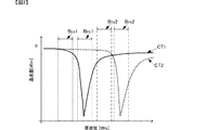
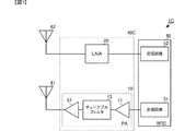
送信回路51は、第1送信信号を生成して、高周波パワーアンプ10に出力する。第1高周波増幅器11は、第1送信信号を増幅して出力する。第1高周波増幅器11は、少なくとも2つ以上の通信バンドに対応する広帯域の高周波増幅器であるので、第1送信信号の所定周波数帯域Btx1(送信周波数帯域)の周波数成分のみでなく、第1送信信号の所定周波数帯域Brx1(受信周波数帯域)の周波数成分も増幅してしまう。この全周波数帯域に亘って信号レベルが増幅された第1送信信号は、チューナブルフィルタ13に入力される。
送信回路51は、第2送信信号を生成して、高周波パワーアンプ10に出力する。第1高周波増幅器11は、第2送信信号を増幅して出力する。第1高周波増幅器11は、広帯域対応の高周波増幅器であるので、第2送信信号の周波数帯域Btx2(送信周波数帯域)の周波数成分のみでなく、第2送信信号の周波数帯域Brx2(受信周波数帯域)の周波数成分も増幅してしまう。この全周波数帯域に亘って信号レベルが増幅された第2送信信号は、チューナブルフィルタ13に入力される。
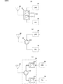
10,10A,10B:高周波パワーアンプ
11,11B:第1高周波増幅器
12:終段高周波増幅器
13:チューナブルフィルタ
14:第1のアイソレータ
15:第2のアイソレータ
20:LNA
30:分波器
40,40C:高周波フロントエンド回路
50:RFIC
51:送信回路
52:受信回路
60:アンテナ
111,112:単位増幅器
310:デュプレクサ
311,312,331,332:周波数可変フィルタ
320,330:サーキュレータ
Claims (6)
- 第1の高周波増幅器と、
該第1の高周波増幅器の後段に接続される終段の高周波増幅器と、
前記第1の高周波増幅器と前記終段の高周波増幅器との間に接続されたチューナブルフィルタと、
アイソレータと、
を備え、
前記第1の高周波増幅器と前記終段の高周波増幅器は、複数の通信バンドの送信信号を増幅可能なマルチモード/マルチバンドの高周波増幅器であり、
前記チューナブルフィルタは、
前記複数の通信バンドのうち第1通信バンドを構成する第1送信信号の周波数帯域を通過帯域とし、前記第1通信バンドを構成する第1受信信号の周波数帯域を減衰帯域とする第1制御態様と、
前記複数の通信バンドのうち前記第1通信バンドと異なる第2通信バンドを構成する第2送信信号の周波数帯域を通過帯域とし、前記第2通信バンドを構成する第2受信信号の周波数帯域を減衰帯域とする第2制御態様とを切り替えるものであり、
前記アイソレータは、
前記第1の高周波増幅器と前記チューナブルフィルタとの間、あるいは、
前記チューナブルフィルタと前記終段の高周波増幅器との間の少なくとも一方に接続されている、
高周波パワーアンプ。 - 前記第1送信信号または前記第2送信信号の周波数帯域は、複数の送信変調帯域を含み、
前記チューナブルフィルタは、前記複数の送信変調帯域のうち使用する送信変調帯域のみを通過帯域とする、
請求項1に記載の高周波パワーアンプ。 - 前記アイソレータは、
前記第1の高周波増幅器と前記チューナブルフィルタとの間に接続された第1のアイソレータと、
前記チューナブルフィルタと前記終段の高周波増幅器との間に接続された第2のアイソレータと、を備える、
請求項1または請求項2に記載の高周波パワーアンプ。 - 前記第1の高周波増幅器は複数の単位増幅器で構成されており、
前記終段の高周波増幅器と、前記第1の高周波増幅器における前記複数の単位増幅器のうち前記終段の高周波増幅器に最も近い単位増幅器との間に、前記チューナブルフィルタが接続されている、
請求項1乃至請求項3のいずれかに記載の高周波パワーアンプ。 - 請求項1乃至請求項4のいずれかに記載の高周波パワーアンプと、
第1個別端子から入力した高周波信号を共通端子に出力し、前記共通端子から入力された高周波信号を第2個別端子に出力し、前記高周波パワーアンプが第1個別端子に接続された分波器と、
前記第2個別端子に接続され、前記分波器からの高周波信号を増幅する高周波増幅回路と、を備える、
高周波フロントエンド回路。 - 請求項5に記載の高周波フロントエンド回路と、
前記共通端子に接続するアンテナと、
前記高周波パワーアンプに接続する送信回路、および、前記分波器からの高周波信号を増幅する高周波増幅回路に接続する受信回路を有するRFICと、
を備えた、無線通信装置。
Applications Claiming Priority (3)
| Application Number | Priority Date | Filing Date | Title |
|---|---|---|---|
| JP2013199163 | 2013-09-26 | ||
| JP2013199163 | 2013-09-26 | ||
| PCT/JP2014/067329 WO2015045538A1 (ja) | 2013-09-26 | 2014-06-30 | 高周波パワーアンプ、高周波フロントエンド回路、無線通信装置 |
Publications (2)
| Publication Number | Publication Date |
|---|---|
| JPWO2015045538A1 JPWO2015045538A1 (ja) | 2017-03-09 |
| JP6288099B2 true JP6288099B2 (ja) | 2018-03-07 |
Family
ID=52742696
Family Applications (1)
| Application Number | Title | Priority Date | Filing Date |
|---|---|---|---|
| JP2015538963A Active JP6288099B2 (ja) | 2013-09-26 | 2014-06-30 | 高周波パワーアンプ、高周波フロントエンド回路、無線通信装置 |
Country Status (4)
| Country | Link |
|---|---|
| US (1) | US9787334B2 (ja) |
| JP (1) | JP6288099B2 (ja) |
| CN (1) | CN105580283B (ja) |
| WO (1) | WO2015045538A1 (ja) |
Families Citing this family (4)
| Publication number | Priority date | Publication date | Assignee | Title |
|---|---|---|---|---|
| KR102723240B1 (ko) * | 2017-12-07 | 2024-10-31 | 인피니언 테크놀로지스 아게 | 무선 주파수 필터를 위한 시스템 및 방법 |
| KR102088773B1 (ko) * | 2019-01-11 | 2020-03-16 | (주) 기산텔레콤 | 사이드밴드 신호를 억압한 멀티밴드 와이파이 액세스포인트 |
| WO2021039083A1 (ja) * | 2019-08-28 | 2021-03-04 | 株式会社村田製作所 | 高周波モジュール及び通信装置 |
| WO2026004207A1 (ja) * | 2024-06-28 | 2026-01-02 | 株式会社村田製作所 | 高周波回路及び通信装置 |
Family Cites Families (18)
| Publication number | Priority date | Publication date | Assignee | Title |
|---|---|---|---|---|
| US5796772A (en) | 1991-05-13 | 1998-08-18 | Omnipoint Corporation | Multi-band, multi-mode spread-spectrum communication system |
| IL114924A (en) | 1994-08-18 | 2000-02-17 | Omnipoint Corp | Multi-land multi-mode communication system |
| JP3438414B2 (ja) * | 1995-06-09 | 2003-08-18 | 松下電器産業株式会社 | 増幅回路 |
| KR100534159B1 (ko) | 1995-06-09 | 2006-01-27 | 마쯔시다덴기산교 가부시키가이샤 | 증폭기 |
| JP2000115016A (ja) * | 1998-10-08 | 2000-04-21 | Kokusai Electric Co Ltd | 全二重無線機とその回り込み防止方法 |
| US6489862B1 (en) * | 2000-10-03 | 2002-12-03 | Agilent Technologies, Inc. | Method for reducing noise generated in a power amplifier |
| KR100541895B1 (ko) | 2001-09-21 | 2006-01-16 | 가부시끼가이샤 도시바 | 고주파 필터 |
| JP3854212B2 (ja) * | 2002-03-29 | 2006-12-06 | 株式会社東芝 | 高周波フィルタ |
| JP2004194097A (ja) * | 2002-12-12 | 2004-07-08 | Hitachi Kokusai Electric Inc | 全二重無線機 |
| US7444124B1 (en) * | 2003-05-14 | 2008-10-28 | Marvell International Ltd. | Adjustable segmented power amplifier |
| KR100605172B1 (ko) * | 2003-12-15 | 2006-07-28 | 삼성전자주식회사 | 무선인식 기능을 가진 휴대용 단말장치와 휴대용단말장치의 사용방법 |
| US7340237B2 (en) * | 2005-07-25 | 2008-03-04 | Integrated System Solution Corp. | Dual-band active filter |
| US20100197257A1 (en) | 2009-02-04 | 2010-08-05 | Qualcomm Incorporated | Adjustable receive filter responsive to frequency spectrum information |
| US8204444B2 (en) | 2009-02-04 | 2012-06-19 | Qualcomm Incorporated | Adjustable transmission filter responsive to internal sadio status |
| JP2011182271A (ja) | 2010-03-03 | 2011-09-15 | Nec Corp | 無線送信回路、無線通信機器及びそれらに用いる無線送信回路の構成方法 |
| US9065504B2 (en) | 2011-10-28 | 2015-06-23 | Broadcom Corporation | Transmitter front end with programmable notch filter and methods for use therewith |
| JP2013110619A (ja) * | 2011-11-22 | 2013-06-06 | Mitsubishi Electric Corp | 増幅器 |
| US8977216B2 (en) * | 2012-03-19 | 2015-03-10 | Qualcomm Incorporated | Limited Q factor tunable front end using tunable circuits and microelectromechanical system (MEMS) |
-
2014
- 2014-06-30 CN CN201480053087.7A patent/CN105580283B/zh active Active
- 2014-06-30 JP JP2015538963A patent/JP6288099B2/ja active Active
- 2014-06-30 WO PCT/JP2014/067329 patent/WO2015045538A1/ja not_active Ceased
-
2016
- 2016-03-25 US US15/081,474 patent/US9787334B2/en active Active
Also Published As
| Publication number | Publication date |
|---|---|
| WO2015045538A1 (ja) | 2015-04-02 |
| CN105580283A (zh) | 2016-05-11 |
| JPWO2015045538A1 (ja) | 2017-03-09 |
| US9787334B2 (en) | 2017-10-10 |
| CN105580283B (zh) | 2018-10-23 |
| US20160211871A1 (en) | 2016-07-21 |
Similar Documents
| Publication | Publication Date | Title |
|---|---|---|
| CN110048735B (zh) | 用于射频滤波器的系统和方法 | |
| JP6500913B2 (ja) | 高周波回路部品および通信装置 | |
| US11677427B2 (en) | Radio-frequency front-end circuit and communication apparatus | |
| JP6470373B2 (ja) | インピーダンス整合部品を備えたダイバーシティ受信器フロントエンドシステム | |
| KR102041721B1 (ko) | 복합형 필터 장치, 고주파 프론트 엔드 회로 및 통신 장치 | |
| US10128796B2 (en) | Power amplification module and front end circuit | |
| WO2017119062A1 (ja) | ドハティ増幅器 | |
| JP2012089995A (ja) | 移動通信端末用モジュール、及び移動通信端末 | |
| JP2018098578A (ja) | 通信モジュール | |
| KR20160051640A (ko) | 스위칭 네트워크를 갖는 다이버시티 수신기 프론트 엔드 시스템 | |
| JPWO2015045538A1 (ja) | 高周波パワーアンプ、高周波フロントエンド回路、無線通信装置 | |
| JP2012257030A (ja) | 信号切替装置 | |
| CN104348497A (zh) | 一种无线通讯信号接收装置及方法 | |
| JP6428184B2 (ja) | 高周波フロントエンド回路、高周波モジュール | |
| CN113196675A (zh) | 高频模块和通信装置 | |
| KR101400739B1 (ko) | 무전기 간섭신호 제거 장치 | |
| JP2019029996A (ja) | 複合型フィルタ装置、高周波フロントエンド回路および通信装置 | |
| JP6424891B2 (ja) | 送信回路、高周波フロントエンド回路、送信信号の制御方法、および、高周波フロントエンドの送受信制御方法 | |
| JP2018157248A (ja) | フロントエンドモジュール | |
| KR20060082444A (ko) | 무선 송수신기에서 노이즈를 제거하는 장치 및 방법 | |
| WO2020202891A1 (ja) | 高周波モジュール及び通信装置 | |
| US12328130B2 (en) | Radio frequency module and communication device | |
| KR100986517B1 (ko) | 무선통신장치 | |
| JP2009060511A (ja) | 通信装置 | |
| WO2013108677A1 (ja) | 電力増幅回路 |
Legal Events
| Date | Code | Title | Description |
|---|---|---|---|
| A521 | Request for written amendment filed |
Free format text: JAPANESE INTERMEDIATE CODE: A523 Effective date: 20161201 |
|
| A521 | Request for written amendment filed |
Free format text: JAPANESE INTERMEDIATE CODE: A523 Effective date: 20161222 |
|
| A02 | Decision of refusal |
Free format text: JAPANESE INTERMEDIATE CODE: A02 Effective date: 20170704 |
|
| A521 | Request for written amendment filed |
Free format text: JAPANESE INTERMEDIATE CODE: A523 Effective date: 20170929 |
|
| A911 | Transfer to examiner for re-examination before appeal (zenchi) |
Free format text: JAPANESE INTERMEDIATE CODE: A911 Effective date: 20171011 |
|
| TRDD | Decision of grant or rejection written | ||
| A01 | Written decision to grant a patent or to grant a registration (utility model) |
Free format text: JAPANESE INTERMEDIATE CODE: A01 Effective date: 20180109 |
|
| A61 | First payment of annual fees (during grant procedure) |
Free format text: JAPANESE INTERMEDIATE CODE: A61 Effective date: 20180122 |
|
| R150 | Certificate of patent or registration of utility model |
Ref document number: 6288099 Country of ref document: JP Free format text: JAPANESE INTERMEDIATE CODE: R150 |