JP6317465B2 - 導電性バリア層の選択的形成 - Google Patents
導電性バリア層の選択的形成 Download PDFInfo
- Publication number
- JP6317465B2 JP6317465B2 JP2016553825A JP2016553825A JP6317465B2 JP 6317465 B2 JP6317465 B2 JP 6317465B2 JP 2016553825 A JP2016553825 A JP 2016553825A JP 2016553825 A JP2016553825 A JP 2016553825A JP 6317465 B2 JP6317465 B2 JP 6317465B2
- Authority
- JP
- Japan
- Prior art keywords
- layer
- barrier layer
- semiconductor device
- interconnect
- doped
- Prior art date
- Legal status (The legal status is an assumption and is not a legal conclusion. Google has not performed a legal analysis and makes no representation as to the accuracy of the status listed.)
- Active
Links
Images


Classifications
-
- H—ELECTRICITY
- H10—SEMICONDUCTOR DEVICES; ELECTRIC SOLID-STATE DEVICES NOT OTHERWISE PROVIDED FOR
- H10W—GENERIC PACKAGES, INTERCONNECTIONS, CONNECTORS OR OTHER CONSTRUCTIONAL DETAILS OF DEVICES COVERED BY CLASS H10
- H10W20/00—Interconnections in chips, wafers or substrates
- H10W20/01—Manufacture or treatment
- H10W20/031—Manufacture or treatment of conductive parts of the interconnections
- H10W20/032—Manufacture or treatment of conductive parts of the interconnections of conductive barrier, adhesion or liner layers
- H10W20/033—Manufacture or treatment of conductive parts of the interconnections of conductive barrier, adhesion or liner layers in openings in dielectrics
-
- H—ELECTRICITY
- H10—SEMICONDUCTOR DEVICES; ELECTRIC SOLID-STATE DEVICES NOT OTHERWISE PROVIDED FOR
- H10W—GENERIC PACKAGES, INTERCONNECTIONS, CONNECTORS OR OTHER CONSTRUCTIONAL DETAILS OF DEVICES COVERED BY CLASS H10
- H10W20/00—Interconnections in chips, wafers or substrates
- H10W20/01—Manufacture or treatment
- H10W20/031—Manufacture or treatment of conductive parts of the interconnections
- H10W20/032—Manufacture or treatment of conductive parts of the interconnections of conductive barrier, adhesion or liner layers
- H10W20/033—Manufacture or treatment of conductive parts of the interconnections of conductive barrier, adhesion or liner layers in openings in dielectrics
- H10W20/036—Manufacture or treatment of conductive parts of the interconnections of conductive barrier, adhesion or liner layers in openings in dielectrics the barrier, adhesion or liner layers being within a main fill metal
-
- H—ELECTRICITY
- H10—SEMICONDUCTOR DEVICES; ELECTRIC SOLID-STATE DEVICES NOT OTHERWISE PROVIDED FOR
- H10W—GENERIC PACKAGES, INTERCONNECTIONS, CONNECTORS OR OTHER CONSTRUCTIONAL DETAILS OF DEVICES COVERED BY CLASS H10
- H10W20/00—Interconnections in chips, wafers or substrates
- H10W20/01—Manufacture or treatment
- H10W20/031—Manufacture or treatment of conductive parts of the interconnections
- H10W20/032—Manufacture or treatment of conductive parts of the interconnections of conductive barrier, adhesion or liner layers
- H10W20/047—Manufacture or treatment of conductive parts of the interconnections of conductive barrier, adhesion or liner layers by introducing additional elements therein
-
- H—ELECTRICITY
- H10—SEMICONDUCTOR DEVICES; ELECTRIC SOLID-STATE DEVICES NOT OTHERWISE PROVIDED FOR
- H10W—GENERIC PACKAGES, INTERCONNECTIONS, CONNECTORS OR OTHER CONSTRUCTIONAL DETAILS OF DEVICES COVERED BY CLASS H10
- H10W20/00—Interconnections in chips, wafers or substrates
- H10W20/01—Manufacture or treatment
- H10W20/031—Manufacture or treatment of conductive parts of the interconnections
- H10W20/032—Manufacture or treatment of conductive parts of the interconnections of conductive barrier, adhesion or liner layers
- H10W20/047—Manufacture or treatment of conductive parts of the interconnections of conductive barrier, adhesion or liner layers by introducing additional elements therein
- H10W20/048—Manufacture or treatment of conductive parts of the interconnections of conductive barrier, adhesion or liner layers by introducing additional elements therein by using plasmas or gaseous environments, e.g. by nitriding
-
- H—ELECTRICITY
- H10—SEMICONDUCTOR DEVICES; ELECTRIC SOLID-STATE DEVICES NOT OTHERWISE PROVIDED FOR
- H10W—GENERIC PACKAGES, INTERCONNECTIONS, CONNECTORS OR OTHER CONSTRUCTIONAL DETAILS OF DEVICES COVERED BY CLASS H10
- H10W20/00—Interconnections in chips, wafers or substrates
- H10W20/01—Manufacture or treatment
- H10W20/031—Manufacture or treatment of conductive parts of the interconnections
- H10W20/032—Manufacture or treatment of conductive parts of the interconnections of conductive barrier, adhesion or liner layers
- H10W20/047—Manufacture or treatment of conductive parts of the interconnections of conductive barrier, adhesion or liner layers by introducing additional elements therein
- H10W20/049—Manufacture or treatment of conductive parts of the interconnections of conductive barrier, adhesion or liner layers by introducing additional elements therein by diffusing alloying elements
-
- H—ELECTRICITY
- H10—SEMICONDUCTOR DEVICES; ELECTRIC SOLID-STATE DEVICES NOT OTHERWISE PROVIDED FOR
- H10W—GENERIC PACKAGES, INTERCONNECTIONS, CONNECTORS OR OTHER CONSTRUCTIONAL DETAILS OF DEVICES COVERED BY CLASS H10
- H10W20/00—Interconnections in chips, wafers or substrates
- H10W20/01—Manufacture or treatment
- H10W20/031—Manufacture or treatment of conductive parts of the interconnections
- H10W20/032—Manufacture or treatment of conductive parts of the interconnections of conductive barrier, adhesion or liner layers
- H10W20/052—Manufacture or treatment of conductive parts of the interconnections of conductive barrier, adhesion or liner layers by treatments not introducing additional elements therein
- H10W20/0526—Manufacture or treatment of conductive parts of the interconnections of conductive barrier, adhesion or liner layers by treatments not introducing additional elements therein by thermal treatment thereof
-
- H—ELECTRICITY
- H10—SEMICONDUCTOR DEVICES; ELECTRIC SOLID-STATE DEVICES NOT OTHERWISE PROVIDED FOR
- H10W—GENERIC PACKAGES, INTERCONNECTIONS, CONNECTORS OR OTHER CONSTRUCTIONAL DETAILS OF DEVICES COVERED BY CLASS H10
- H10W20/00—Interconnections in chips, wafers or substrates
- H10W20/01—Manufacture or treatment
- H10W20/031—Manufacture or treatment of conductive parts of the interconnections
- H10W20/056—Manufacture or treatment of conductive parts of the interconnections by filling conductive material into holes, grooves or trenches
- H10W20/057—Manufacture or treatment of conductive parts of the interconnections by filling conductive material into holes, grooves or trenches by selectively depositing, e.g. by using selective CVD or plating
-
- H—ELECTRICITY
- H10—SEMICONDUCTOR DEVICES; ELECTRIC SOLID-STATE DEVICES NOT OTHERWISE PROVIDED FOR
- H10W—GENERIC PACKAGES, INTERCONNECTIONS, CONNECTORS OR OTHER CONSTRUCTIONAL DETAILS OF DEVICES COVERED BY CLASS H10
- H10W20/00—Interconnections in chips, wafers or substrates
- H10W20/01—Manufacture or treatment
- H10W20/071—Manufacture or treatment of dielectric parts thereof
- H10W20/074—Manufacture or treatment of dielectric parts thereof of dielectric parts comprising thin functional dielectric layers, e.g. dielectric etch-stop, barrier, capping or liner layers
- H10W20/076—Manufacture or treatment of dielectric parts thereof of dielectric parts comprising thin functional dielectric layers, e.g. dielectric etch-stop, barrier, capping or liner layers in via holes or trenches
-
- H—ELECTRICITY
- H10—SEMICONDUCTOR DEVICES; ELECTRIC SOLID-STATE DEVICES NOT OTHERWISE PROVIDED FOR
- H10W—GENERIC PACKAGES, INTERCONNECTIONS, CONNECTORS OR OTHER CONSTRUCTIONAL DETAILS OF DEVICES COVERED BY CLASS H10
- H10W20/00—Interconnections in chips, wafers or substrates
- H10W20/40—Interconnections external to wafers or substrates, e.g. back-end-of-line [BEOL] metallisations or vias connecting to gate electrodes
- H10W20/41—Interconnections external to wafers or substrates, e.g. back-end-of-line [BEOL] metallisations or vias connecting to gate electrodes characterised by their conductive parts
- H10W20/42—Vias, e.g. via plugs
-
- H—ELECTRICITY
- H10—SEMICONDUCTOR DEVICES; ELECTRIC SOLID-STATE DEVICES NOT OTHERWISE PROVIDED FOR
- H10W—GENERIC PACKAGES, INTERCONNECTIONS, CONNECTORS OR OTHER CONSTRUCTIONAL DETAILS OF DEVICES COVERED BY CLASS H10
- H10W20/00—Interconnections in chips, wafers or substrates
- H10W20/40—Interconnections external to wafers or substrates, e.g. back-end-of-line [BEOL] metallisations or vias connecting to gate electrodes
- H10W20/41—Interconnections external to wafers or substrates, e.g. back-end-of-line [BEOL] metallisations or vias connecting to gate electrodes characterised by their conductive parts
- H10W20/425—Barrier, adhesion or liner layers
Landscapes
- Internal Circuitry In Semiconductor Integrated Circuit Devices (AREA)
- Physics & Mathematics (AREA)
- Engineering & Computer Science (AREA)
- Plasma & Fusion (AREA)
- Formation Of Insulating Films (AREA)
Description
本出願は、2014年2月28日にJeffrey Junhao Xu等の名義で出願した米国仮特許出願第61/946520号の利益を主張するものであり、その開示全体が参照により本明細書に明示的に組み込まれる。
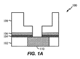
102 第1の酸化物層
104 中間層
106 キャップ層
108 第2の酸化物層
110 第1の相互接続層
112 バリア層
114 第2の相互接続層
120 デバイス
130 デバイス
200 デバイス
202 導電性層
300 デバイス
302 トレンチ
304 ビア、ビア開口
306 処理されたバリア層
308 ドープ導電性層
310 デバイス
330 デバイス
340 デバイス
400 導電性バリア層の選択的形成プロセス
500 ワイヤレス通信システム
520 遠隔ユニット
525A ICデバイス
525B ICデバイス
525C ICデバイス
530 遠隔ユニット
540 基地局
550 遠隔ユニット
580 順方向リンク信号
590 逆方向リンク信号
600 設計用ワークステーション
601 ハードディスク
602 ディスプレイ
603 ドライブ装置
604 記憶媒体
610 回路、回路デザイン
612 半導体構成要素
Claims (12)
- 第1の相互接続層をトレンチに結合させるビアを含むダイと、
前記トレンチの側壁および隣接する表面上、ならびに前記ビアの側壁上の、バリア層であって、前記第1の相互接続層の表面の直接上に第1の側壁部分および第2の側壁部分を含む、バリア層と、
前記第1の相互接続層の前記表面の直上のドープ導電性層であって、前記ビアの向かい合う側壁上の前記バリア層の前記第1の側壁部分と前記第2の側壁部分との間に延在するドープ導電性層と、
前記ビアと前記トレンチの両方内の前記バリア層上の導電性材料であって、前記ドープ導電性層の、前記第1の相互接続層の前記表面とは反対側の表面の直上に配設された導電性材料と
前記第1の相互接続層の一部と重なるエッチストップ層と、
を備え、
前記導電性材料は銅を含み、前記第1の側壁部分及び前記第2の側壁部分の前記バリア層は酸化アルミニウムを含み、前記ドープ導電性層が銅アルミニウム合金を含み、
前記エッチストップ層は中間層とキャップ層とを含み、
前記中間層は炭素ドープ窒化シリコン又は酸素ドープ窒化シリコンからなり、前記キャップ層は非ドープ二酸化シリコンからなる、半導体デバイス。 - 前記導電性材料が銅およびアルミニウムを含む、請求項1に記載の半導体デバイス。
- 前記エッチストップ層は窒素含有シリコンオキシカーバイド(SiCON)を含む、請求項1に記載の半導体デバイス。
- 前記第1の相互接続層が銅を含む、請求項1に記載の半導体デバイス。
- 前記ドープ導電性層がまた、前記導電性材料と前記第1の相互接続層の前記表面との間に延在する、請求項1に記載の半導体デバイス。
- 音楽プレーヤ、ビデオプレーヤ、エンターテインメントユニット、ナビゲーションデバイス、通信デバイス、携帯情報端末(PDA)、固定位置データユニット、およびコンピュータのうちの少なくとも1つに組み込まれる、請求項1に記載の半導体デバイス。
- 第1の相互接続層をトレンチに結合させるビアを含むダイと、
前記トレンチの側壁および隣接する表面上、ならびに前記ビアの側壁上の、バリア層であって、前記第1の相互接続層の表面の直上に第1の側壁部分および第2の側壁部分を含む、バリア層と、
前記第1の相互接続層の前記表面の直上のドープ導電性層であって、前記ビアの向かい合う側壁上の前記バリア層の前記第1の側壁部分と前記第2の側壁部分との間に延在するドープ導電性層と、
前記ビアと前記トレンチの両方内の前記バリア層上の導電するための手段であって、前記ドープ導電性層の、前記第1の相互接続層の前記表面とは反対側の表面の直上にある、導電するための手段と
前記第1の相互接続層の一部と重なるエッチストップ層と、
を備え、
前記導電するための手段が銅を含み、前記第1の側壁部分及び前記第2の側壁部分の前記バリア層が酸化アルミニウムを含み、前記ドープ導電性層が銅アルミニウム合金を含み、
前記エッチストップ層は中間層とキャップ層とを含み、
前記中間層は炭素ドープ窒化シリコン又は酸素ドープ窒化シリコンからなり、前記キャップ層は非ドープ二酸化シリコンからなる、半導体デバイス。 - 前記導電するための手段が銅およびアルミニウムを含む、請求項7に記載の半導体デバイス。
- 前記エッチストップ層が窒素含有シリコンオキシカーバイド(SiCON)を含む、請求項7に記載の半導体デバイス。
- 前記第1の相互接続層が銅を含む、請求項7に記載の半導体デバイス。
- 前記ドープ導電性層がまた、前記ビアの前記側壁間に延在する、請求項7に記載の半導体デバイス。
- 音楽プレーヤ、ビデオプレーヤ、エンターテインメントユニット、ナビゲーションデバイス、通信デバイス、携帯情報端末(PDA)、固定位置データユニット、およびコンピュータのうちの少なくとも1つに組み込まれる、請求項7に記載の半導体デバイス。
Applications Claiming Priority (5)
| Application Number | Priority Date | Filing Date | Title |
|---|---|---|---|
| US201461946520P | 2014-02-28 | 2014-02-28 | |
| US61/946,520 | 2014-02-28 | ||
| US14/274,099 US9343357B2 (en) | 2014-02-28 | 2014-05-09 | Selective conductive barrier layer formation |
| US14/274,099 | 2014-05-09 | ||
| PCT/US2015/016621 WO2015130549A2 (en) | 2014-02-28 | 2015-02-19 | Selective conductive barrier layer formation |
Publications (2)
| Publication Number | Publication Date |
|---|---|
| JP2017508290A JP2017508290A (ja) | 2017-03-23 |
| JP6317465B2 true JP6317465B2 (ja) | 2018-04-25 |
Family
ID=54007111
Family Applications (1)
| Application Number | Title | Priority Date | Filing Date |
|---|---|---|---|
| JP2016553825A Active JP6317465B2 (ja) | 2014-02-28 | 2015-02-19 | 導電性バリア層の選択的形成 |
Country Status (5)
| Country | Link |
|---|---|
| US (2) | US9343357B2 (ja) |
| EP (1) | EP3111473A2 (ja) |
| JP (1) | JP6317465B2 (ja) |
| CN (1) | CN106030792B (ja) |
| WO (1) | WO2015130549A2 (ja) |
Families Citing this family (22)
| Publication number | Priority date | Publication date | Assignee | Title |
|---|---|---|---|---|
| CN104979329B (zh) * | 2014-04-10 | 2018-08-10 | 中芯国际集成电路制造(上海)有限公司 | 一种半导体器件及其制造方法和电子装置 |
| US9543248B2 (en) * | 2015-01-21 | 2017-01-10 | Qualcomm Incorporated | Integrated circuit devices and methods |
| US9564489B2 (en) * | 2015-06-29 | 2017-02-07 | Taiwan Semiconductor Manufacturing Company, Ltd. | Multiple gate field-effect transistors having oxygen-scavenged gate stack |
| US10541204B2 (en) | 2015-10-20 | 2020-01-21 | Taiwan Semiconductor Manufacturing Co., Ltd. | Interconnection structure and method of forming the same |
| US10153351B2 (en) * | 2016-01-29 | 2018-12-11 | Taiwan Semiconductor Manufacturing Co., Ltd. | Semiconductor device and a method for fabricating the same |
| DE102016125299B4 (de) | 2016-01-29 | 2024-10-02 | Taiwan Semiconductor Manufacturing Co., Ltd. | Halbleitervorrichtung und Verfahren zu ihrer Herstellung |
| US9761526B2 (en) * | 2016-02-03 | 2017-09-12 | Globalfoundries Inc. | Interconnect structure having tungsten contact copper wiring |
| US10361121B2 (en) * | 2016-05-13 | 2019-07-23 | Intel Corporation | Aluminum oxide for thermal management or adhesion |
| US11127629B2 (en) * | 2016-05-17 | 2021-09-21 | Taiwan Semiconductor Manufacturing Company Ltd. | Semiconductor device and fabricating method thereof |
| US10332903B2 (en) * | 2016-12-19 | 2019-06-25 | Macronix International Co., Ltd. | Multi-layer structure and a method for manufacturing the same and a corresponding contact structure |
| CN108242386B (zh) * | 2016-12-23 | 2020-06-02 | 旺宏电子股份有限公司 | 多层结构与其制造方法及对应其的接触结构 |
| US10763168B2 (en) | 2017-11-17 | 2020-09-01 | Taiwan Semiconductor Manufacturing Co., Ltd. | Semiconductor structure with doped via plug and method for forming the same |
| US11623246B2 (en) | 2018-02-26 | 2023-04-11 | Invensense, Inc. | Piezoelectric micromachined ultrasound transducer device with piezoelectric barrier layer |
| US11245040B2 (en) * | 2018-03-02 | 2022-02-08 | Semiconductor Energy Laboratory Co., Ltd. | Semiconductor device and method for manufacturing semiconductor device |
| JPWO2019171196A1 (ja) | 2018-03-07 | 2021-02-25 | 株式会社半導体エネルギー研究所 | 半導体装置、および半導体装置の作製方法 |
| US10741477B2 (en) * | 2018-03-23 | 2020-08-11 | Taiwan Semiconductor Manufacturing Co., Ltd. | Semiconductor devices and methods of forming the same |
| WO2020084415A1 (ja) * | 2018-10-26 | 2020-04-30 | 株式会社半導体エネルギー研究所 | 半導体装置、および半導体装置の作製方法 |
| JP2021044502A (ja) | 2019-09-13 | 2021-03-18 | キオクシア株式会社 | 半導体装置およびその製造方法 |
| US11610811B2 (en) | 2020-06-16 | 2023-03-21 | Nanya Technology Corporation | Semiconductor device with covering liners and method for fabricating the same |
| US12424552B2 (en) * | 2021-09-24 | 2025-09-23 | Nanya Technology Corporation | Semiconductor structure and method of manufacturing thereof |
| US12557686B2 (en) | 2022-11-11 | 2026-02-17 | Stmicroelectronics S.R.L. | Semiconductor package or device with barrier layer |
| US20250054853A1 (en) * | 2023-08-08 | 2025-02-13 | Amkor Technology Singapore Holding Pte. Ltd. | Semiconductor devices methods of manufacturing semiconductor devices |
Family Cites Families (27)
| Publication number | Priority date | Publication date | Assignee | Title |
|---|---|---|---|---|
| US5633199A (en) * | 1995-11-02 | 1997-05-27 | Motorola Inc. | Process for fabricating a metallized interconnect structure in a semiconductor device |
| JP3400353B2 (ja) | 1998-05-28 | 2003-04-28 | 株式会社東芝 | 半導体装置の製造方法 |
| JP3974284B2 (ja) | 1999-03-18 | 2007-09-12 | 株式会社東芝 | 半導体装置の製造方法 |
| KR100386034B1 (ko) | 2000-12-06 | 2003-06-02 | 에이에스엠 마이크로케미스트리 리미티드 | 확산 방지막의 결정립계를 금속산화물로 충진한 구리 배선구조의 반도체 소자 제조 방법 |
| JP2003173929A (ja) | 2001-09-26 | 2003-06-20 | Mitsui Mining & Smelting Co Ltd | キャパシタ層形成用の積層板及びその製造方法 |
| US6833321B2 (en) * | 2001-11-30 | 2004-12-21 | Intel Corporation | Method of making a semiconductor device that has copper damascene interconnects with enhanced electromigration reliability |
| JP3648480B2 (ja) | 2001-12-26 | 2005-05-18 | 株式会社東芝 | 半導体装置およびその製造方法 |
| US7235884B1 (en) * | 2003-04-01 | 2007-06-26 | Altera Corporation | Local control of electrical and mechanical properties of copper interconnects to achieve stable and reliable via |
| KR100562650B1 (ko) * | 2004-06-25 | 2006-03-20 | 주식회사 하이닉스반도체 | 반도체 소자 제조 방법 |
| US7456093B2 (en) * | 2004-07-03 | 2008-11-25 | Taiwan Semiconductor Manufacturing Co., Ltd. | Method for improving a semiconductor device delamination resistance |
| US7223691B2 (en) * | 2004-10-14 | 2007-05-29 | International Business Machines Corporation | Method of forming low resistance and reliable via in inter-level dielectric interconnect |
| JP2006216809A (ja) | 2005-02-04 | 2006-08-17 | Matsushita Electric Ind Co Ltd | 半導体装置及びその製造方法 |
| JP2007109736A (ja) * | 2005-10-11 | 2007-04-26 | Nec Electronics Corp | 半導体装置およびその製造方法 |
| JP2007173511A (ja) | 2005-12-22 | 2007-07-05 | Sony Corp | 半導体装置の製造方法 |
| JP5162869B2 (ja) * | 2006-09-20 | 2013-03-13 | 富士通セミコンダクター株式会社 | 半導体装置およびその製造方法 |
| KR100808601B1 (ko) | 2006-12-28 | 2008-02-29 | 주식회사 하이닉스반도체 | 다마신 공정을 이용한 반도체 소자의 다층 금속배선형성방법 |
| JP5089244B2 (ja) * | 2007-05-22 | 2012-12-05 | ローム株式会社 | 半導体装置 |
| JP2009147137A (ja) * | 2007-12-14 | 2009-07-02 | Toshiba Corp | 半導体装置およびその製造方法 |
| US8476758B2 (en) * | 2008-01-09 | 2013-07-02 | International Business Machines Corporation | Airgap-containing interconnect structure with patternable low-k material and method of fabricating |
| WO2009117670A2 (en) * | 2008-03-21 | 2009-09-24 | President And Fellows Of Harvard College | Self-aligned barrier layers for interconnects |
| US7821107B2 (en) | 2008-04-22 | 2010-10-26 | Micron Technology, Inc. | Die stacking with an annular via having a recessed socket |
| US7727883B2 (en) * | 2008-09-30 | 2010-06-01 | Tokyo Electron Limited | Method of forming a diffusion barrier and adhesion layer for an interconnect structure |
| JP2010141024A (ja) | 2008-12-10 | 2010-06-24 | Renesas Technology Corp | 半導体装置の製造方法および半導体装置 |
| AU2010310750B2 (en) * | 2009-10-23 | 2015-02-26 | President And Fellows Of Harvard College | Self-aligned barrier and capping layers for interconnects |
| JP6009152B2 (ja) * | 2011-09-15 | 2016-10-19 | ルネサスエレクトロニクス株式会社 | 半導体装置の製造方法 |
| WO2014013941A1 (ja) | 2012-07-18 | 2014-01-23 | 東京エレクトロン株式会社 | 半導体装置の製造方法 |
| US9082824B2 (en) * | 2013-05-31 | 2015-07-14 | Freescale Semiconductor, Inc. | Method for forming an electrical connection between metal layers |
-
2014
- 2014-05-09 US US14/274,099 patent/US9343357B2/en active Active
-
2015
- 2015-02-19 JP JP2016553825A patent/JP6317465B2/ja active Active
- 2015-02-19 WO PCT/US2015/016621 patent/WO2015130549A2/en not_active Ceased
- 2015-02-19 CN CN201580009551.7A patent/CN106030792B/zh not_active Expired - Fee Related
- 2015-02-19 EP EP15718278.3A patent/EP3111473A2/en not_active Withdrawn
-
2016
- 2016-04-19 US US15/133,040 patent/US20160233126A1/en not_active Abandoned
Also Published As
| Publication number | Publication date |
|---|---|
| US20160233126A1 (en) | 2016-08-11 |
| CN106030792B (zh) | 2017-09-22 |
| CN106030792A (zh) | 2016-10-12 |
| JP2017508290A (ja) | 2017-03-23 |
| US9343357B2 (en) | 2016-05-17 |
| US20150249038A1 (en) | 2015-09-03 |
| WO2015130549A2 (en) | 2015-09-03 |
| WO2015130549A3 (en) | 2015-11-12 |
| EP3111473A2 (en) | 2017-01-04 |
Similar Documents
| Publication | Publication Date | Title |
|---|---|---|
| JP6317465B2 (ja) | 導電性バリア層の選択的形成 | |
| US10879107B2 (en) | Method of forming barrier free contact for metal interconnects | |
| CN109616456B (zh) | 形成自对准帽的方法和设备 | |
| US20240087953A1 (en) | Metal Contact Structure and Method of Forming the Same in a Semiconductor Device | |
| TWI618189B (zh) | 金屬互連件裝置及形成金屬互連件的方法 | |
| US10276634B2 (en) | Semiconductor memory structure with magnetic tunnel junction (MTJ) cell | |
| JP2010258213A (ja) | 半導体装置及び半導体装置の製造方法 | |
| TWI423412B (zh) | 半導體裝置 | |
| TW201535728A (zh) | 集成電路結構及其製造方法 | |
| KR102421731B1 (ko) | 반도체 소자의 배선 형성 방법 | |
| JP2011003883A (ja) | 半導体装置の製造方法 | |
| TW201013794A (en) | Microelectronic device | |
| TW201342528A (zh) | 用於鑲嵌式圖案化之avd硬遮罩 | |
| CN107004636B (zh) | 通孔材料选择和处理 | |
| JP6224844B2 (ja) | 導電層ルーティング | |
| CN101640184A (zh) | 半导体器件及其制造方法 | |
| US9941156B2 (en) | Systems and methods to reduce parasitic capacitance | |
| CN104934368B (zh) | 形成自对准帽的方法和设备 | |
| US9478490B2 (en) | Capacitor from second level middle-of-line layer in combination with decoupling capacitors | |
| KR101758617B1 (ko) | 반도체 소자의 제조방법 |
Legal Events
| Date | Code | Title | Description |
|---|---|---|---|
| A521 | Request for written amendment filed |
Free format text: JAPANESE INTERMEDIATE CODE: A523 Effective date: 20160824 |
|
| A621 | Written request for application examination |
Free format text: JAPANESE INTERMEDIATE CODE: A621 Effective date: 20160824 |
|
| A871 | Explanation of circumstances concerning accelerated examination |
Free format text: JAPANESE INTERMEDIATE CODE: A871 Effective date: 20160824 |
|
| A975 | Report on accelerated examination |
Free format text: JAPANESE INTERMEDIATE CODE: A971005 Effective date: 20170201 |
|
| A131 | Notification of reasons for refusal |
Free format text: JAPANESE INTERMEDIATE CODE: A131 Effective date: 20170206 |
|
| A601 | Written request for extension of time |
Free format text: JAPANESE INTERMEDIATE CODE: A601 Effective date: 20170502 |
|
| A521 | Request for written amendment filed |
Free format text: JAPANESE INTERMEDIATE CODE: A523 Effective date: 20170804 |
|
| A131 | Notification of reasons for refusal |
Free format text: JAPANESE INTERMEDIATE CODE: A131 Effective date: 20170915 |
|
| A521 | Request for written amendment filed |
Free format text: JAPANESE INTERMEDIATE CODE: A523 Effective date: 20171213 |
|
| TRDD | Decision of grant or rejection written | ||
| A01 | Written decision to grant a patent or to grant a registration (utility model) |
Free format text: JAPANESE INTERMEDIATE CODE: A01 Effective date: 20180305 |
|
| A61 | First payment of annual fees (during grant procedure) |
Free format text: JAPANESE INTERMEDIATE CODE: A61 Effective date: 20180329 |
|
| R150 | Certificate of patent or registration of utility model |
Ref document number: 6317465 Country of ref document: JP Free format text: JAPANESE INTERMEDIATE CODE: R150 |