JP6385677B2 - 基板加工方法 - Google Patents
基板加工方法 Download PDFInfo
- Publication number
- JP6385677B2 JP6385677B2 JP2014007690A JP2014007690A JP6385677B2 JP 6385677 B2 JP6385677 B2 JP 6385677B2 JP 2014007690 A JP2014007690 A JP 2014007690A JP 2014007690 A JP2014007690 A JP 2014007690A JP 6385677 B2 JP6385677 B2 JP 6385677B2
- Authority
- JP
- Japan
- Prior art keywords
- substrate
- film
- carrier
- thermosetting
- adhesive film
- Prior art date
- Legal status (The legal status is an assumption and is not a legal conclusion. Google has not performed a legal analysis and makes no representation as to the accuracy of the status listed.)
- Active
Links
Images







Classifications
-
- H—ELECTRICITY
- H10—SEMICONDUCTOR DEVICES; ELECTRIC SOLID-STATE DEVICES NOT OTHERWISE PROVIDED FOR
- H10P—GENERIC PROCESSES OR APPARATUS FOR THE MANUFACTURE OR TREATMENT OF DEVICES COVERED BY CLASS H10
- H10P50/00—Etching of wafers, substrates or parts of devices
-
- H—ELECTRICITY
- H10—SEMICONDUCTOR DEVICES; ELECTRIC SOLID-STATE DEVICES NOT OTHERWISE PROVIDED FOR
- H10P—GENERIC PROCESSES OR APPARATUS FOR THE MANUFACTURE OR TREATMENT OF DEVICES COVERED BY CLASS H10
- H10P95/00—Generic processes or apparatus for manufacture or treatments not covered by the other groups of this subclass
-
- H—ELECTRICITY
- H10—SEMICONDUCTOR DEVICES; ELECTRIC SOLID-STATE DEVICES NOT OTHERWISE PROVIDED FOR
- H10P—GENERIC PROCESSES OR APPARATUS FOR THE MANUFACTURE OR TREATMENT OF DEVICES COVERED BY CLASS H10
- H10P14/00—Formation of materials, e.g. in the shape of layers or pillars
- H10P14/20—Formation of materials, e.g. in the shape of layers or pillars of semiconductor materials
-
- H—ELECTRICITY
- H10—SEMICONDUCTOR DEVICES; ELECTRIC SOLID-STATE DEVICES NOT OTHERWISE PROVIDED FOR
- H10P—GENERIC PROCESSES OR APPARATUS FOR THE MANUFACTURE OR TREATMENT OF DEVICES COVERED BY CLASS H10
- H10P70/00—Cleaning of wafers, substrates or parts of devices
- H10P70/20—Cleaning during device manufacture
-
- H—ELECTRICITY
- H10—SEMICONDUCTOR DEVICES; ELECTRIC SOLID-STATE DEVICES NOT OTHERWISE PROVIDED FOR
- H10P—GENERIC PROCESSES OR APPARATUS FOR THE MANUFACTURE OR TREATMENT OF DEVICES COVERED BY CLASS H10
- H10P72/00—Handling or holding of wafers, substrates or devices during manufacture or treatment thereof
- H10P72/70—Handling or holding of wafers, substrates or devices during manufacture or treatment thereof for supporting or gripping
- H10P72/74—Handling or holding of wafers, substrates or devices during manufacture or treatment thereof for supporting or gripping using temporarily an auxiliary support
-
- H—ELECTRICITY
- H10—SEMICONDUCTOR DEVICES; ELECTRIC SOLID-STATE DEVICES NOT OTHERWISE PROVIDED FOR
- H10P—GENERIC PROCESSES OR APPARATUS FOR THE MANUFACTURE OR TREATMENT OF DEVICES COVERED BY CLASS H10
- H10P72/00—Handling or holding of wafers, substrates or devices during manufacture or treatment thereof
- H10P72/70—Handling or holding of wafers, substrates or devices during manufacture or treatment thereof for supporting or gripping
- H10P72/74—Handling or holding of wafers, substrates or devices during manufacture or treatment thereof for supporting or gripping using temporarily an auxiliary support
- H10P72/7448—Handling or holding of wafers, substrates or devices during manufacture or treatment thereof for supporting or gripping using temporarily an auxiliary support the bond interface between the auxiliary support and the wafer comprising two or more, e.g. multilayer adhesive or adhesive and release layer
-
- H—ELECTRICITY
- H10—SEMICONDUCTOR DEVICES; ELECTRIC SOLID-STATE DEVICES NOT OTHERWISE PROVIDED FOR
- H10P—GENERIC PROCESSES OR APPARATUS FOR THE MANUFACTURE OR TREATMENT OF DEVICES COVERED BY CLASS H10
- H10P72/00—Handling or holding of wafers, substrates or devices during manufacture or treatment thereof
- H10P72/70—Handling or holding of wafers, substrates or devices during manufacture or treatment thereof for supporting or gripping
- H10P72/74—Handling or holding of wafers, substrates or devices during manufacture or treatment thereof for supporting or gripping using temporarily an auxiliary support
- H10P72/7402—Wafer tapes, e.g. grinding or dicing support tapes
-
- H—ELECTRICITY
- H10—SEMICONDUCTOR DEVICES; ELECTRIC SOLID-STATE DEVICES NOT OTHERWISE PROVIDED FOR
- H10P—GENERIC PROCESSES OR APPARATUS FOR THE MANUFACTURE OR TREATMENT OF DEVICES COVERED BY CLASS H10
- H10P72/00—Handling or holding of wafers, substrates or devices during manufacture or treatment thereof
- H10P72/70—Handling or holding of wafers, substrates or devices during manufacture or treatment thereof for supporting or gripping
- H10P72/74—Handling or holding of wafers, substrates or devices during manufacture or treatment thereof for supporting or gripping using temporarily an auxiliary support
- H10P72/7412—Handling or holding of wafers, substrates or devices during manufacture or treatment thereof for supporting or gripping using temporarily an auxiliary support the auxiliary support including means facilitating the separation of a device or wafer from the auxiliary support
-
- H—ELECTRICITY
- H10—SEMICONDUCTOR DEVICES; ELECTRIC SOLID-STATE DEVICES NOT OTHERWISE PROVIDED FOR
- H10P—GENERIC PROCESSES OR APPARATUS FOR THE MANUFACTURE OR TREATMENT OF DEVICES COVERED BY CLASS H10
- H10P72/00—Handling or holding of wafers, substrates or devices during manufacture or treatment thereof
- H10P72/70—Handling or holding of wafers, substrates or devices during manufacture or treatment thereof for supporting or gripping
- H10P72/74—Handling or holding of wafers, substrates or devices during manufacture or treatment thereof for supporting or gripping using temporarily an auxiliary support
- H10P72/7416—Handling or holding of wafers, substrates or devices during manufacture or treatment thereof for supporting or gripping using temporarily an auxiliary support used during dicing or grinding
-
- H—ELECTRICITY
- H10—SEMICONDUCTOR DEVICES; ELECTRIC SOLID-STATE DEVICES NOT OTHERWISE PROVIDED FOR
- H10P—GENERIC PROCESSES OR APPARATUS FOR THE MANUFACTURE OR TREATMENT OF DEVICES COVERED BY CLASS H10
- H10P72/00—Handling or holding of wafers, substrates or devices during manufacture or treatment thereof
- H10P72/70—Handling or holding of wafers, substrates or devices during manufacture or treatment thereof for supporting or gripping
- H10P72/74—Handling or holding of wafers, substrates or devices during manufacture or treatment thereof for supporting or gripping using temporarily an auxiliary support
- H10P72/7422—Handling or holding of wafers, substrates or devices during manufacture or treatment thereof for supporting or gripping using temporarily an auxiliary support used to protect an active side of a device or wafer
-
- H—ELECTRICITY
- H10—SEMICONDUCTOR DEVICES; ELECTRIC SOLID-STATE DEVICES NOT OTHERWISE PROVIDED FOR
- H10P—GENERIC PROCESSES OR APPARATUS FOR THE MANUFACTURE OR TREATMENT OF DEVICES COVERED BY CLASS H10
- H10P72/00—Handling or holding of wafers, substrates or devices during manufacture or treatment thereof
- H10P72/70—Handling or holding of wafers, substrates or devices during manufacture or treatment thereof for supporting or gripping
- H10P72/74—Handling or holding of wafers, substrates or devices during manufacture or treatment thereof for supporting or gripping using temporarily an auxiliary support
- H10P72/744—Details of chemical or physical process used for separating the auxiliary support from a device or a wafer
-
- H—ELECTRICITY
- H10—SEMICONDUCTOR DEVICES; ELECTRIC SOLID-STATE DEVICES NOT OTHERWISE PROVIDED FOR
- H10W—GENERIC PACKAGES, INTERCONNECTIONS, CONNECTORS OR OTHER CONSTRUCTIONAL DETAILS OF DEVICES COVERED BY CLASS H10
- H10W72/00—Interconnections or connectors in packages
- H10W72/01—Manufacture or treatment
- H10W72/019—Manufacture or treatment of bond pads
- H10W72/01904—Manufacture or treatment of bond pads using temporary auxiliary members, e.g. using sacrificial coatings or handle substrates
-
- H—ELECTRICITY
- H10—SEMICONDUCTOR DEVICES; ELECTRIC SOLID-STATE DEVICES NOT OTHERWISE PROVIDED FOR
- H10W—GENERIC PACKAGES, INTERCONNECTIONS, CONNECTORS OR OTHER CONSTRUCTIONAL DETAILS OF DEVICES COVERED BY CLASS H10
- H10W72/00—Interconnections or connectors in packages
- H10W72/01—Manufacture or treatment
- H10W72/019—Manufacture or treatment of bond pads
- H10W72/01951—Changing the shapes of bond pads
-
- H—ELECTRICITY
- H10—SEMICONDUCTOR DEVICES; ELECTRIC SOLID-STATE DEVICES NOT OTHERWISE PROVIDED FOR
- H10W—GENERIC PACKAGES, INTERCONNECTIONS, CONNECTORS OR OTHER CONSTRUCTIONAL DETAILS OF DEVICES COVERED BY CLASS H10
- H10W72/00—Interconnections or connectors in packages
- H10W72/01—Manufacture or treatment
- H10W72/0198—Manufacture or treatment batch processes
-
- H—ELECTRICITY
- H10—SEMICONDUCTOR DEVICES; ELECTRIC SOLID-STATE DEVICES NOT OTHERWISE PROVIDED FOR
- H10W—GENERIC PACKAGES, INTERCONNECTIONS, CONNECTORS OR OTHER CONSTRUCTIONAL DETAILS OF DEVICES COVERED BY CLASS H10
- H10W72/00—Interconnections or connectors in packages
- H10W72/071—Connecting or disconnecting
- H10W72/072—Connecting or disconnecting of bump connectors
-
- H—ELECTRICITY
- H10—SEMICONDUCTOR DEVICES; ELECTRIC SOLID-STATE DEVICES NOT OTHERWISE PROVIDED FOR
- H10W—GENERIC PACKAGES, INTERCONNECTIONS, CONNECTORS OR OTHER CONSTRUCTIONAL DETAILS OF DEVICES COVERED BY CLASS H10
- H10W72/00—Interconnections or connectors in packages
- H10W72/071—Connecting or disconnecting
- H10W72/072—Connecting or disconnecting of bump connectors
- H10W72/07251—Connecting or disconnecting of bump connectors characterised by changes in properties of the bump connectors during connecting
- H10W72/07254—Connecting or disconnecting of bump connectors characterised by changes in properties of the bump connectors during connecting changes in dispositions
-
- H—ELECTRICITY
- H10—SEMICONDUCTOR DEVICES; ELECTRIC SOLID-STATE DEVICES NOT OTHERWISE PROVIDED FOR
- H10W—GENERIC PACKAGES, INTERCONNECTIONS, CONNECTORS OR OTHER CONSTRUCTIONAL DETAILS OF DEVICES COVERED BY CLASS H10
- H10W72/00—Interconnections or connectors in packages
- H10W72/20—Bump connectors, e.g. solder bumps or copper pillars; Dummy bumps; Thermal bumps
- H10W72/241—Dispositions, e.g. layouts
- H10W72/244—Dispositions, e.g. layouts relative to underlying supporting features, e.g. bond pads, RDLs or vias
-
- H—ELECTRICITY
- H10—SEMICONDUCTOR DEVICES; ELECTRIC SOLID-STATE DEVICES NOT OTHERWISE PROVIDED FOR
- H10W—GENERIC PACKAGES, INTERCONNECTIONS, CONNECTORS OR OTHER CONSTRUCTIONAL DETAILS OF DEVICES COVERED BY CLASS H10
- H10W72/00—Interconnections or connectors in packages
- H10W72/20—Bump connectors, e.g. solder bumps or copper pillars; Dummy bumps; Thermal bumps
- H10W72/241—Dispositions, e.g. layouts
- H10W72/247—Dispositions of multiple bumps
-
- H—ELECTRICITY
- H10—SEMICONDUCTOR DEVICES; ELECTRIC SOLID-STATE DEVICES NOT OTHERWISE PROVIDED FOR
- H10W—GENERIC PACKAGES, INTERCONNECTIONS, CONNECTORS OR OTHER CONSTRUCTIONAL DETAILS OF DEVICES COVERED BY CLASS H10
- H10W72/00—Interconnections or connectors in packages
- H10W72/20—Bump connectors, e.g. solder bumps or copper pillars; Dummy bumps; Thermal bumps
- H10W72/29—Bond pads specially adapted therefor
-
- H—ELECTRICITY
- H10—SEMICONDUCTOR DEVICES; ELECTRIC SOLID-STATE DEVICES NOT OTHERWISE PROVIDED FOR
- H10W—GENERIC PACKAGES, INTERCONNECTIONS, CONNECTORS OR OTHER CONSTRUCTIONAL DETAILS OF DEVICES COVERED BY CLASS H10
- H10W90/00—Package configurations
- H10W90/20—Configurations of stacked chips
- H10W90/26—Configurations of stacked chips the stacked chips being of the same size without any chips being laterally offset, e.g. chip stacks having a rectangular shape
-
- H—ELECTRICITY
- H10—SEMICONDUCTOR DEVICES; ELECTRIC SOLID-STATE DEVICES NOT OTHERWISE PROVIDED FOR
- H10W—GENERIC PACKAGES, INTERCONNECTIONS, CONNECTORS OR OTHER CONSTRUCTIONAL DETAILS OF DEVICES COVERED BY CLASS H10
- H10W90/00—Package configurations
- H10W90/20—Configurations of stacked chips
- H10W90/297—Configurations of stacked chips characterised by the through-semiconductor vias [TSVs] in the stacked chips
-
- H—ELECTRICITY
- H10—SEMICONDUCTOR DEVICES; ELECTRIC SOLID-STATE DEVICES NOT OTHERWISE PROVIDED FOR
- H10W—GENERIC PACKAGES, INTERCONNECTIONS, CONNECTORS OR OTHER CONSTRUCTIONAL DETAILS OF DEVICES COVERED BY CLASS H10
- H10W90/00—Package configurations
- H10W90/701—Package configurations characterised by the relative positions of pads or connectors relative to package parts
- H10W90/721—Package configurations characterised by the relative positions of pads or connectors relative to package parts of bump connectors
- H10W90/722—Package configurations characterised by the relative positions of pads or connectors relative to package parts of bump connectors between stacked chips
-
- H—ELECTRICITY
- H10—SEMICONDUCTOR DEVICES; ELECTRIC SOLID-STATE DEVICES NOT OTHERWISE PROVIDED FOR
- H10W—GENERIC PACKAGES, INTERCONNECTIONS, CONNECTORS OR OTHER CONSTRUCTIONAL DETAILS OF DEVICES COVERED BY CLASS H10
- H10W90/00—Package configurations
- H10W90/701—Package configurations characterised by the relative positions of pads or connectors relative to package parts
- H10W90/721—Package configurations characterised by the relative positions of pads or connectors relative to package parts of bump connectors
- H10W90/724—Package configurations characterised by the relative positions of pads or connectors relative to package parts of bump connectors between a chip and a stacked insulating package substrate, interposer or RDL
-
- H—ELECTRICITY
- H10—SEMICONDUCTOR DEVICES; ELECTRIC SOLID-STATE DEVICES NOT OTHERWISE PROVIDED FOR
- H10W—GENERIC PACKAGES, INTERCONNECTIONS, CONNECTORS OR OTHER CONSTRUCTIONAL DETAILS OF DEVICES COVERED BY CLASS H10
- H10W99/00—Subject matter not provided for in other groups of this subclass
Landscapes
- Mechanical Treatment Of Semiconductor (AREA)
- Adhesives Or Adhesive Processes (AREA)
- Chemical Vapour Deposition (AREA)
- Encapsulation Of And Coatings For Semiconductor Or Solid State Devices (AREA)
- Container, Conveyance, Adherence, Positioning, Of Wafer (AREA)
Description
本発明の他の目的はキャリヤを基板から容易に分離できる基板加工方法を提供することである。
前記化学気相蒸着は前記ヘキサメチルジシロキサン(HMDSO)を反応ガスとして使用して行うことができる。
一実施形態の方法において、前記結合膜を提供する段階は、前記第1及び第2剥離膜と前記熱硬化性接着膜とを硬化させる段階をさらに含むことができる。
一実施形態の方法において、前記熱硬化性接着膜をプラズマ処理する段階は、酸素、窒素、アルゴンの中で少なくともいずれか1つを含むプラズマによって前記第2剥離膜の残留物を前記熱硬化性接着膜から除去する段階を包含することができる。
前記熱硬化性接着膜は、前記基板及び前記キャリヤの露出された縁と接触することができる。
他の実施形態の方法において、前記熱硬化性第1剥離膜と前記熱硬化性第2剥離膜との中で少なくともいずれか1つは、ポリジメチルシロキサン(PDMS)とヘキサメチルジシロキサン(HMDSO)との中で少なくともいずれか1つを包含することができる。前記熱硬化性接着膜は、シロキサン(siloxane)を包含することができる。
他の実施形態の方法において、前記熱硬化性第1剥離膜を除去する段階は、前記薄形化された基板を洗浄する段階を包含することができる。
その他の実施形態の方法において、前記結合膜を提供する段階は、前記結合膜を熱に露出させて前記結合膜を強化させる段階を包含することができる。
前記クラックを形成する段階は、前記熱硬化性接着膜の側面にブレードにより衝撃を加える段階を包含することができる。
本発明と従来技術とを比較した長所は添付された図面を参照した詳細な説明と特許請求の範囲を通じて明確になり得る。特に、本発明は特許請求の範囲で明確に請求される。しかし、本発明は添付された図面に関連して次の詳細な説明を参照することによって最も良く理解することができる。図面において、同一の参照符号は多様な図面を通じて同一の構成要素を示す。
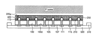
図1A乃至図1Pは本発明の一実施形態による基板加工方法を示した断面図である。図1C、図1E及び図1Iは図1B、図1D及び図1Hの一部を各々示した断面図である。図1F及び図1Gは図1Bの変形形態を示した断面図である。

接着膜250は第1剥離膜210上に前記化学式を有するシリコン(silicone)或いはこれを含む熱硬化性樹脂(resin)をコーティングして形成することができる。一例として、接着膜250はシロキサン(siloxane)系列の物質で形成することができる。他の例として、接着膜250はトリプロピレンメラミン(TMAT:tripropylenemelamine)或いはこれを含む物質で形成することができる。
第1剥離膜210の厚さTr1が厚いほど、接着膜250をウエハ100から分離するのに必要である力は低くなり得る。第1剥離膜210の厚さTr1は第1前駆体膜211の厚さTp1及び/又はプラズマ化学気相蒸着条件によって異なり得る。
プラズマ強度が強いほど、プラズマ時間が長いほど、第1剥離膜210は硬く(hard)なり得る。これと異なり、プラズマ強度が弱いほど、プラズマ時間が短いほど、第1剥離膜210は軟らか(soft)になり得る。第1剥離膜210があまりにも硬くなれば、第1剥離膜210の自己剥離(self−delamination)やクラック(crack)が生じる恐れがあり、あまりにも軟らかになれば、第1剥離膜210が液相状態に留まって容易に剥がれてしまう。前述のプラズマ蒸着条件によれば、完全架橋結合された(fully cross−linked)或いはこれと類似な構造を有する安定的な第1剥離膜210が形成され得る。
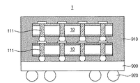
図1Qは本発明の一実施形態による基板加工方法を利用する半導体チップの製造方法を示した断面図である。図1Rは本発明の一実施形態による基板加工方法を利用する半導体パッケージの製造方法を示した断面図である。
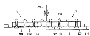
図1Qを参照すれば、ウエハ100を複数個の半導体チップ10に分離することができる。カッティングホィール800によってウエハ100のスクライブレーンを切断することによってウエハ100を複数個の半導体チップ10に分離するウエハ切断(wafer sawing)工程を進行することができる。このようにウエハ100から分離された複数個の半導体チップ10の中で少なくとも1つをパッケージングすることができる。他の例として、レーザ或いはその他のカッティング器具を利用して前記ウエハ切断工程を進行することができる。
図2A乃至図2Fは本発明の他の実施形態による基板加工方法を示した断面図である。図2Dは図2Cの一部を拡大示した断面図である。
図2Aを参照すれば、ウエハ100の活性面100a上に第1剥離膜210と接着膜250とを形成することができる。例えば、ウエハ100の活性面100a上に熱硬化性物質をスピンコーティングし、プラズマ化学気相蒸着した後、パターニングして第1剥離膜210を形成することができる。前記パターニングによって第1剥離膜210はウエハ100の縁100eを露出させ得る。接着膜250は第1剥離膜210上に形成され、ウエハ100の縁100eと結合され得る。
他の例として、図1Fのように接着膜250はキャリヤ300上に形成され得る。その他の例として、図1Gのようにウエハ100とキャリヤ300との上に第1接着膜250aと第2接着膜250bとが各々形成され得る。
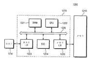
図3Aは本発明の実施形態による基板加工方法を通じて得られた半導体装置を具備するメモリカードを示したブロック図である。図3Bは本発明の実施形態による基板加工方法を通じて得られた半導体装置を応用した情報処理システムを示したブロック図である。
100・・・基板
105・・・集積回路
111・・・貫通電極
113・・・バンプ
200・・・結合膜
210・・・第1剥離膜
220・・・第2剥離膜
250・・・接着膜
300・・・キャリヤ
400・・・イニシエータ
500・・・保護テープ
600・・・ローリングテープ
700・・・スプレ
800・・・カッティングホィール
900・・・印刷回路基板
910・・・モールド膜
920・・・外部端子
Claims (19)
- 基板とキャリヤとの間に前記基板と前記キャリヤとを結合するために、第1表面及び第1表面に対向する第2表面を有する熱硬化性接着膜と前記熱硬化性接着膜の第1表面上に提供され基板の表面と接触する第1剥離膜と第2表面上に直に提供されキャリヤの表面に接触する第2剥離膜とを含む結合膜を提供する段階と、
前記キャリヤによって前記基板が支持された状態で前記基板を加工する段階と、
前記結合膜を除去して前記基板を前記キャリヤから分離する段階と、を有し、
前記結合膜を提供する段階は、
前記基板上に第1熱硬化性物質を提供して前記第1剥離膜を形成する段階と、
前記キャリヤ上に第2熱硬化性物質を提供して前記第2剥離膜を形成する段階と、
前記基板及び前記キャリヤの中で少なくともいずれか1つの上に第3熱硬化性物質を提供して前記熱硬化性接着膜を形成する段階と、を含み、
前記第1剥離膜を形成する段階は、
シリコンを含む前駆体を前記基板上にコーティングして前駆体膜を形成する段階と、
化学気相蒸着で前記前駆体膜上にシリコンを含む蒸着膜を形成する段階と、を含み、
前記基板を前記キャリヤから分離する段階は、
前記熱硬化性接着膜の側面に物理的な接触方法でクラックを形成する段階を含み、
前記基板は前記基板の表面に形成された複数のバンプを含み、
前記第1剥離膜は前記複数のバンプ及び前記複数のバンプ間の前記基板の表面の上に形成され、
前記熱硬化性接着膜の側面は前記熱硬化性接着膜の第1表面及び第2表面に接続されることを含むことを特徴とする基板加工方法。 - 前記基板と前記結合膜との間の結合力は前記キャリヤと前記結合膜との間の結合力に比べて大きいことを特徴とする請求項1に記載の基板加工方法。
- 前記前駆体は、ポリジメチルシロキサン(PDMS)とヘキサメチルジシロキサン(HMDSO)とを含み、
前記化学気相蒸着は前記ヘキサメチルジシロキサン(HMDSO)を反応ガスとして使用して行うことを特徴とする請求項1に記載の基板加工方法。 - 前記第2剥離膜を形成する段階は、
ポリジメチルシロキサン(PDMS)とヘキサメチルジシロキサン(HMDSO)とを含む前駆体を前記キャリヤ上にコーティングして前駆体膜を形成する段階と、
前記ヘキサメチルジシロキサン(HMDSO)と酸素を反応ガスとして使用した化学気相蒸着で前記前駆体膜上に蒸着膜を形成する段階と、を含むことを特徴とする請求項1に記載の基板加工方法。 - 前記熱硬化性接着膜を形成する段階は、
前記第1剥離膜と前記第2剥離膜との中で少なくとも1つ上にシロキサン(siloxane)或いは前記シロキサンを含む熱硬化性物質をコーティングする段階を含むことを特徴とする請求項1に記載の基板加工方法。 - 前記結合膜を提供する段階は、
前記第1及び第2剥離膜と前記熱硬化性接着膜を硬化させる段階をさらに含むことを特徴とする請求項1に記載の基板加工方法。 - 前記基板を前記キャリヤから分離する段階は、
前記キャリヤを前記熱硬化性接着膜から分離する段階と、
前記熱硬化性接着膜をプラズマ処理する段階と、
前記熱硬化性接着膜を前記基板から分離する段階と、
前記基板を洗浄する段階と、をさらに含むことを特徴とする請求項1に記載の基板加工方法。 - 前記熱硬化性接着膜をプラズマ処理する段階は、
酸素、窒素、アルゴンの中で少なくともいずれか1つを含むプラズマで前記第2剥離膜の残留物を前記熱硬化性接着膜から除去する段階を含むことを特徴とする請求項7に記載の基板加工方法。 - 前記結合膜を提供する段階は、
前記基板上に第1熱硬化性物質を提供して前記第1剥離膜を形成し、そして前記基板の縁を露出させる段階と、
前記キャリヤ上に第2熱硬化性物質を提供して前記第2剥離膜を形成し、そして前記キャリヤの縁を露出させる段階と、
前記基板及び前記キャリヤの中で少なくともいずれか1つ上に第3熱硬化性物質を提供して前記熱硬化性接着膜を形成する段階と、を含み、
前記熱硬化性接着膜は、前記基板及び前記キャリヤの露出された縁と接触することを特徴とする請求項1に記載の基板加工方法。 - 基板上に直に熱硬化性第1剥離膜を形成する段階と、
キャリヤ上に熱硬化性第2剥離膜を形成する段階と、
前記基板と前記キャリヤとの間に前記基板を前記キャリヤに結合するために、第1表面が前記熱硬化性第1剥離膜に接着され前記第1表面と対向する第2表面が前記熱硬化性第2剥離膜と直に接着される熱硬化性接着膜を提供する段階と、
前記キャリヤによって支持された状態で前記基板を薄形化する段階と、
前記キャリヤを前記薄形化された基板から分離する段階と、
前記熱硬化性接着膜上の前記熱硬化性第2剥離膜を除去するために、前記熱硬化性接着膜をプラズマ処理する段階と、
前記熱硬化性接着膜を前記薄形化された基板から分離する段階と、
前記薄形化された基板から前記熱硬化性第1剥離膜を除去する段階と、を有し、
前記熱硬化性第1剥離膜を形成する段階は、
シリコンを含む前駆体を前記基板上にコーティングして前駆体膜を形成する段階と、
化学気相蒸着で前記前駆体膜上にシリコンを含む蒸着膜を形成する段階と、を含み、
前記キャリヤを前記薄形化された基板から分離する段階は、
前記熱硬化性接着膜の側面にクラックを形成するために前記熱硬化性接着膜の側面に物理的な応力を加える段階と、
前記熱硬化性接着膜から前記キャリヤを分離する段階と、を含むことを特徴とする基板加工方法。 - 前記基板を薄形化する段階は、
前記基板の中で前記熱硬化性第1剥離膜が形成された第1面の反対面である第2面をリセスする段階を含み、
前記薄形化された基板のリセスされた第2面を通じて前記基板に含まれた少なくとも一つの貫通電極が露出されることを特徴とする請求項10に記載の基板加工方法。 - 前記熱硬化性第1剥離膜と前記熱硬化性第2剥離膜との中で少なくともいずれか1つは、ポリジメチルシロキサン(PDMS)とヘキサメチルジシロキサン(HMDSO)との中で少なくともいずれか1つを含み、前記熱硬化性接着膜は、シロキサン(siloxane)を含むことを特徴とする請求項10に記載の基板加工方法。
- 前記基板の上に複数のバンプを形成する段階をさらに含み、
前記熱硬化性第1剥離膜は直に前記複数のバンプ及び基板の上に形成され、
前記基板は、複数個のバンプと前記バンプと電気的に連結された複数個の貫通電極を含む半導体ウエハであり、そして前記キャリヤは、前記基板と同一な物質或いはガラスを含むことを特徴とする請求項10に記載の基板加工方法。 - 前記熱硬化性第1剥離膜を除去する段階は、前記薄形化された基板を洗浄する段階を含むことを特徴とする請求項10に記載の基板加工方法。
- 熱硬化性接着膜と熱硬化性接着膜に直に結合され基板の第1面に結合される第1剥離膜と熱硬化性接着膜に直に結合されキャリヤの第1面に直に結合される第2剥離膜とを含み、前記基板との結合力が前記キャリヤとの結合力に比べて大きい結合膜を提供する段階と、
前記結合膜が前記基板と結合され、前記キャリヤが前記結合膜に結合された状態で、前記基板の前記第1面の反対面である前記基板の第2面を加工する段階と、
前記基板から前記結合膜を除去する段階と、を有し、
第1剥離膜は直に前記基板の第1面及び前記基板の第1面上に形成された複数のバンプに結合され、
前記複数のバンプは直に前記基板の貫通電極に接続され、
前記結合膜を除去する段階は、
前記熱硬化性接着膜の側面に物理的な接触方法で前記結合膜から前記キャリヤを分離するためのクラックを形成する段階と、
前記結合膜から前記キャリヤを分離した後に前記基板から少なくとも前記第2剥離膜と前記熱硬化性接着膜とを除去する段階と、を含み、
前記熱硬化性接着膜の側面は前記熱硬化性接着膜の第1表面及び第2表面に接続されることを含むことを特徴とする基板加工方法。 - 前記第1及び第2剥離膜は、熱硬化性物質を含むことを特徴とする請求項15に記載の基板加工方法。
- 前記結合膜を提供する段階は、
前記結合膜を熱に露出させて前記結合膜を強化させる段階を含むことを特徴とする請求項16に記載の基板加工方法。 - 前記熱硬化性接着膜は、前記基板の縁と前記キャリヤの縁との中で少なくともいずれか1つに直接的に結合されることを特徴とする請求項15に記載の基板加工方法。
- 前記クラックを形成する段階は、
前記熱硬化性接着膜の側面にブレードにより衝撃を加える段階を含むことを特徴とする請求項1に記載の基板加工方法。
Applications Claiming Priority (2)
| Application Number | Priority Date | Filing Date | Title |
|---|---|---|---|
| KR1020130008695A KR102077248B1 (ko) | 2013-01-25 | 2013-01-25 | 기판 가공 방법 |
| KR10-2013-0008695 | 2013-01-25 |
Publications (3)
| Publication Number | Publication Date |
|---|---|
| JP2014146793A JP2014146793A (ja) | 2014-08-14 |
| JP2014146793A5 JP2014146793A5 (ja) | 2017-03-30 |
| JP6385677B2 true JP6385677B2 (ja) | 2018-09-05 |
Family
ID=51223376
Family Applications (1)
| Application Number | Title | Priority Date | Filing Date |
|---|---|---|---|
| JP2014007690A Active JP6385677B2 (ja) | 2013-01-25 | 2014-01-20 | 基板加工方法 |
Country Status (3)
| Country | Link |
|---|---|
| US (1) | US9595446B2 (ja) |
| JP (1) | JP6385677B2 (ja) |
| KR (1) | KR102077248B1 (ja) |
Families Citing this family (19)
| Publication number | Priority date | Publication date | Assignee | Title |
|---|---|---|---|---|
| US9064686B2 (en) | 2010-04-15 | 2015-06-23 | Suss Microtec Lithography, Gmbh | Method and apparatus for temporary bonding of ultra thin wafers |
| KR20120082165A (ko) * | 2011-01-13 | 2012-07-23 | 삼성전기주식회사 | 그린 시트 및 이의 제조방법 |
| KR102046534B1 (ko) * | 2013-01-25 | 2019-11-19 | 삼성전자주식회사 | 기판 가공 방법 |
| JP6023737B2 (ja) * | 2014-03-18 | 2016-11-09 | 信越化学工業株式会社 | ウエハ加工体、ウエハ加工用仮接着材、及び薄型ウエハの製造方法 |
| CN106165074B (zh) | 2014-03-19 | 2020-05-12 | 三星电子株式会社 | 制造半导体装置的方法 |
| JP6193813B2 (ja) * | 2014-06-10 | 2017-09-06 | 信越化学工業株式会社 | ウエハ加工用仮接着材料、ウエハ加工体及びこれらを使用する薄型ウエハの製造方法 |
| DE102015000451A1 (de) * | 2015-01-15 | 2016-07-21 | Siltectra Gmbh | Unebener Wafer und Verfahren zum Herstellen eines unebenen Wafers |
| US10894935B2 (en) | 2015-12-04 | 2021-01-19 | Samsung Electronics Co., Ltd. | Composition for removing silicone resins and method of thinning substrate by using the same |
| BR112018015267B1 (pt) | 2016-02-18 | 2023-03-07 | Ecolab Usa Inc | Método e composição para remover sujeiras, rótulos e outro material adesivo de uma superfície |
| JP6691504B2 (ja) * | 2016-05-12 | 2020-04-28 | 信越化学工業株式会社 | ウエハ加工体及びその製造方法並びにウエハ上における有機膜の被覆性確認方法 |
| EP3477685A4 (en) * | 2016-06-22 | 2020-07-01 | Nissan Chemical Corporation | POLYDIMETHYLSILOXANE ADHESIVE |
| WO2018125673A2 (en) | 2016-12-28 | 2018-07-05 | Invensas Bonding Technologies, Inc | Processing stacked substrates |
| WO2019130185A1 (en) * | 2017-12-29 | 2019-07-04 | 3M Innovative Properties Company | Thermally curable two part processing adhesive composition |
| US10964664B2 (en) | 2018-04-20 | 2021-03-30 | Invensas Bonding Technologies, Inc. | DBI to Si bonding for simplified handle wafer |
| SG11202010863YA (en) | 2018-05-01 | 2020-11-27 | Nissan Chemical Corp | Polysiloxane-containing temporary adhesive comprising heat-resistant polymerization inhibitor |
| SG11202101497RA (en) | 2018-10-16 | 2021-03-30 | Showa Denko Kk | Composition, method for cleaning adhesive polymer, method for producing device wafer, and method for regenerating support wafer |
| JP7759027B2 (ja) * | 2020-08-27 | 2025-10-23 | 日産化学株式会社 | 積層体及び剥離剤組成物 |
| US12381170B2 (en) * | 2021-02-15 | 2025-08-05 | Brewer Science, Inc. | Temporary bonding and debonding process to prevent deformation of metal connection in thermocompression bonding |
| US12525572B2 (en) | 2021-03-31 | 2026-01-13 | Adeia Semiconductor Bonding Technologies Inc. | Direct bonding and debonding of carrier |
Family Cites Families (33)
| Publication number | Priority date | Publication date | Assignee | Title |
|---|---|---|---|---|
| US5863832A (en) | 1996-06-28 | 1999-01-26 | Intel Corporation | Capping layer in interconnect system and method for bonding the capping layer onto the interconnect system |
| US6230569B1 (en) | 1999-05-24 | 2001-05-15 | Micron Technology, Inc. | Use of a stream of compressed gas to detect semiconductor interconnect problems |
| JP4137310B2 (ja) * | 1999-09-06 | 2008-08-20 | リンテック株式会社 | 両面粘着シートに固定された物品の剥離方法および剥離装置 |
| US20030107927A1 (en) | 2001-03-12 | 2003-06-12 | Yeda Research And Development Co. Ltd. | Method using a synthetic molecular spring device in a system for dynamically controlling a system property and a corresponding system thereof |
| US7534498B2 (en) * | 2002-06-03 | 2009-05-19 | 3M Innovative Properties Company | Laminate body, method, and apparatus for manufacturing ultrathin substrate using the laminate body |
| JP3832408B2 (ja) | 2002-09-11 | 2006-10-11 | 松下電器産業株式会社 | 半導体装置の製造方法 |
| US20040265531A1 (en) | 2003-06-30 | 2004-12-30 | Mckean Dennis R. | Sliders bonded by a debondable silicon-based encapsulant |
| US20050066995A1 (en) * | 2003-09-30 | 2005-03-31 | International Business Machines Corporation | Non-hermetic encapsulant removal for module rework |
| JPWO2005036633A1 (ja) | 2003-10-07 | 2007-11-22 | 長瀬産業株式会社 | 電子部材の製造方法、及び、接着材付icチップ |
| JP2005129653A (ja) | 2003-10-22 | 2005-05-19 | Fuji Electric Holdings Co Ltd | 半導体装置の製造方法 |
| US7226812B2 (en) * | 2004-03-31 | 2007-06-05 | Intel Corporation | Wafer support and release in wafer processing |
| US7196872B2 (en) | 2004-04-29 | 2007-03-27 | Hitachi Global Storage Netherlands, B.V. | Sliders bonded by a debondable encapsulant comprising different polymers formed via in situ polymerization |
| JP4613709B2 (ja) | 2005-06-24 | 2011-01-19 | セイコーエプソン株式会社 | 半導体装置の製造方法 |
| MY148064A (en) | 2006-10-30 | 2013-02-28 | Sumitomo Bakelite Co | Liquid resin composition, semiconductor wafer having adhesive layer, semiconductor element having adhesive layer, semiconductor package , process for manufacturing semiconductor element and process for manufacturing semiconductor package. |
| JP5196838B2 (ja) * | 2007-04-17 | 2013-05-15 | リンテック株式会社 | 接着剤付きチップの製造方法 |
| DE102007020655A1 (de) * | 2007-04-30 | 2008-11-06 | Fraunhofer-Gesellschaft zur Förderung der angewandten Forschung e.V. | Verfahren zum Herstellen dünner Schichten und entsprechende Schicht |
| US20080302481A1 (en) | 2007-06-07 | 2008-12-11 | Tru-Si Technologies, Inc. | Method and apparatus for debonding of structures which are bonded together, including (but not limited to) debonding of semiconductor wafers from carriers when the bonding is effected by double-sided adhesive tape |
| JP2009141070A (ja) * | 2007-12-05 | 2009-06-25 | Lintec Corp | 剥離装置及び剥離方法 |
| JP2009209345A (ja) | 2008-02-06 | 2009-09-17 | Hitachi Chem Co Ltd | 粘接着シート |
| US8092628B2 (en) | 2008-10-31 | 2012-01-10 | Brewer Science Inc. | Cyclic olefin compositions for temporary wafer bonding |
| US8764026B2 (en) | 2009-04-16 | 2014-07-01 | Suss Microtec Lithography, Gmbh | Device for centering wafers |
| US8871609B2 (en) | 2009-06-30 | 2014-10-28 | Taiwan Semiconductor Manufacturing Company, Ltd. | Thin wafer handling structure and method |
| US8236118B2 (en) | 2009-08-07 | 2012-08-07 | Guardian Industries Corp. | Debonding and transfer techniques for hetero-epitaxially grown graphene, and products including the same |
| US9847243B2 (en) | 2009-08-27 | 2017-12-19 | Corning Incorporated | Debonding a glass substrate from carrier using ultrasonic wave |
| US8398804B2 (en) | 2010-01-11 | 2013-03-19 | Navaid Baqai | Pressure sensitive textile adhesive |
| US8017439B2 (en) | 2010-01-26 | 2011-09-13 | Texas Instruments Incorporated | Dual carrier for joining IC die or wafers to TSV wafers |
| US8852391B2 (en) | 2010-06-21 | 2014-10-07 | Brewer Science Inc. | Method and apparatus for removing a reversibly mounted device wafer from a carrier substrate |
| JP5583080B2 (ja) | 2010-07-07 | 2014-09-03 | 古河電気工業株式会社 | ウエハ加工用テープおよびそれを用いた半導体加工方法 |
| US9263314B2 (en) | 2010-08-06 | 2016-02-16 | Brewer Science Inc. | Multiple bonding layers for thin-wafer handling |
| FR2964048B1 (fr) * | 2010-08-30 | 2012-09-21 | Commissariat Energie Atomique | Procédé de réalisation d'un film, par exemple monocristallin, sur un support en polymère |
| US8313982B2 (en) | 2010-09-20 | 2012-11-20 | Texas Instruments Incorporated | Stacked die assemblies including TSV die |
| JP6001568B2 (ja) * | 2011-02-28 | 2016-10-05 | ダウ コーニング コーポレーションDow Corning Corporation | ウェハ接着システム、及びその接着並びに剥離方法 |
| KR20130000211A (ko) * | 2011-06-22 | 2013-01-02 | 삼성전자주식회사 | 기판 가공 방법 |
-
2013
- 2013-01-25 KR KR1020130008695A patent/KR102077248B1/ko active Active
-
2014
- 2014-01-09 US US14/150,906 patent/US9595446B2/en active Active
- 2014-01-20 JP JP2014007690A patent/JP6385677B2/ja active Active
Also Published As
| Publication number | Publication date |
|---|---|
| US20140213039A1 (en) | 2014-07-31 |
| KR20140095824A (ko) | 2014-08-04 |
| JP2014146793A (ja) | 2014-08-14 |
| KR102077248B1 (ko) | 2020-02-13 |
| US9595446B2 (en) | 2017-03-14 |
Similar Documents
| Publication | Publication Date | Title |
|---|---|---|
| JP6385677B2 (ja) | 基板加工方法 | |
| US9412636B2 (en) | Methods for processing substrates | |
| US20240387439A1 (en) | Direct gang bonding methods and structures | |
| JP6197422B2 (ja) | 半導体装置の製造方法および支持基板付きウェハ | |
| CN102163559B (zh) | 堆叠装置的制造方法及装置晶片处理方法 | |
| JP5334411B2 (ja) | 貼り合わせ基板および貼り合せ基板を用いた半導体装置の製造方法 | |
| US9287222B1 (en) | Integrated semiconductor device and method for fabricating the same | |
| US20120329249A1 (en) | Methods of processing substrates | |
| JP5661928B2 (ja) | 積層体の製造方法、基板の処理方法および積層体 | |
| CN104218022A (zh) | 晶片封装体及其制造方法 | |
| CN103633013B (zh) | 硅通孔封装结构的形成方法 | |
| TWI401752B (zh) | 晶片封裝結構之製造方法 | |
| CN110875268A (zh) | 晶圆级封装方法及封装结构 | |
| CN108242393B (zh) | 一种半导体器件的制造方法 | |
| CN111370360A (zh) | 基底贴膜方法及封装方法 | |
| CN104465581A (zh) | 一种低成本高可靠性芯片尺寸cis封装 | |
| CN111524849A (zh) | 半导体结构及其制作方法 | |
| CN101304015A (zh) | 半导体装置及其制造方法 | |
| CN106409732A (zh) | 一种利用uv实现晶圆与玻璃分离的方法 | |
| CN105762086A (zh) | 焊盘结构的制作方法、键合结构的制作方法及键合结构 | |
| CN109461666B (zh) | 一种芯片封装方法 | |
| CN110534404B (zh) | 半导体装置的制造方法 | |
| CN100536259C (zh) | 制作微型连接器的方法 | |
| US9997390B2 (en) | Semiconductor manufacturing method and laminated body | |
| CN102163558A (zh) | 芯片封装结构的制造方法 |
Legal Events
| Date | Code | Title | Description |
|---|---|---|---|
| RD02 | Notification of acceptance of power of attorney |
Free format text: JAPANESE INTERMEDIATE CODE: A7422 Effective date: 20161222 |
|
| RD04 | Notification of resignation of power of attorney |
Free format text: JAPANESE INTERMEDIATE CODE: A7424 Effective date: 20161228 |
|
| A621 | Written request for application examination |
Free format text: JAPANESE INTERMEDIATE CODE: A621 Effective date: 20170120 |
|
| A521 | Request for written amendment filed |
Free format text: JAPANESE INTERMEDIATE CODE: A523 Effective date: 20170222 |
|
| A977 | Report on retrieval |
Free format text: JAPANESE INTERMEDIATE CODE: A971007 Effective date: 20171124 |
|
| A131 | Notification of reasons for refusal |
Free format text: JAPANESE INTERMEDIATE CODE: A131 Effective date: 20171219 |
|
| A521 | Request for written amendment filed |
Free format text: JAPANESE INTERMEDIATE CODE: A523 Effective date: 20180316 |
|
| TRDD | Decision of grant or rejection written | ||
| A01 | Written decision to grant a patent or to grant a registration (utility model) |
Free format text: JAPANESE INTERMEDIATE CODE: A01 Effective date: 20180710 |
|
| A61 | First payment of annual fees (during grant procedure) |
Free format text: JAPANESE INTERMEDIATE CODE: A61 Effective date: 20180808 |
|
| R150 | Certificate of patent or registration of utility model |
Ref document number: 6385677 Country of ref document: JP Free format text: JAPANESE INTERMEDIATE CODE: R150 |
|
| R250 | Receipt of annual fees |
Free format text: JAPANESE INTERMEDIATE CODE: R250 |
|
| R250 | Receipt of annual fees |
Free format text: JAPANESE INTERMEDIATE CODE: R250 |
|
| R250 | Receipt of annual fees |
Free format text: JAPANESE INTERMEDIATE CODE: R250 |
|
| R250 | Receipt of annual fees |
Free format text: JAPANESE INTERMEDIATE CODE: R250 |
|
| R250 | Receipt of annual fees |
Free format text: JAPANESE INTERMEDIATE CODE: R250 |