JP6431004B2 - Hall sensor and sensor array - Google Patents
Hall sensor and sensor array Download PDFInfo
- Publication number
- JP6431004B2 JP6431004B2 JP2016132964A JP2016132964A JP6431004B2 JP 6431004 B2 JP6431004 B2 JP 6431004B2 JP 2016132964 A JP2016132964 A JP 2016132964A JP 2016132964 A JP2016132964 A JP 2016132964A JP 6431004 B2 JP6431004 B2 JP 6431004B2
- Authority
- JP
- Japan
- Prior art keywords
- hall sensor
- ext
- sensor
- terminals
- hall
- Prior art date
- Legal status (The legal status is an assumption and is not a legal conclusion. Google has not performed a legal analysis and makes no representation as to the accuracy of the status listed.)
- Expired - Fee Related
Links
Images






Classifications
-
- G—PHYSICS
- G01—MEASURING; TESTING
- G01R—MEASURING ELECTRIC VARIABLES; MEASURING MAGNETIC VARIABLES
- G01R33/00—Arrangements or instruments for measuring magnetic variables
- G01R33/02—Measuring direction or magnitude of magnetic fields or magnetic flux
- G01R33/06—Measuring direction or magnitude of magnetic fields or magnetic flux using galvano-magnetic devices
- G01R33/07—Hall effect devices
-
- G—PHYSICS
- G01—MEASURING; TESTING
- G01R—MEASURING ELECTRIC VARIABLES; MEASURING MAGNETIC VARIABLES
- G01R33/00—Arrangements or instruments for measuring magnetic variables
- G01R33/0094—Sensor arrays
-
- G—PHYSICS
- G01—MEASURING; TESTING
- G01R—MEASURING ELECTRIC VARIABLES; MEASURING MAGNETIC VARIABLES
- G01R33/00—Arrangements or instruments for measuring magnetic variables
- G01R33/02—Measuring direction or magnitude of magnetic fields or magnetic flux
- G01R33/06—Measuring direction or magnitude of magnetic fields or magnetic flux using galvano-magnetic devices
- G01R33/07—Hall effect devices
- G01R33/072—Constructional adaptation of the sensor to specific applications
- G01R33/075—Hall devices configured for spinning current measurements
-
- G—PHYSICS
- G01—MEASURING; TESTING
- G01R—MEASURING ELECTRIC VARIABLES; MEASURING MAGNETIC VARIABLES
- G01R33/00—Arrangements or instruments for measuring magnetic variables
- G01R33/02—Measuring direction or magnitude of magnetic fields or magnetic flux
- G01R33/06—Measuring direction or magnitude of magnetic fields or magnetic flux using galvano-magnetic devices
- G01R33/07—Hall effect devices
- G01R33/077—Vertical Hall-effect devices
Landscapes
- Physics & Mathematics (AREA)
- Condensed Matter Physics & Semiconductors (AREA)
- General Physics & Mathematics (AREA)
- Measuring Magnetic Variables (AREA)
- Hall/Mr Elements (AREA)
Description
本発明は、複数のホールセンサ素子を有するホールセンサと、このようなホールセンサを有するセンサ配列体とに関する。 The present invention relates to a hall sensor having a plurality of hall sensor elements and a sensor array having such a hall sensor.
米国の物理学者エドウィン・ハーバート・ホール(1855〜1938年)にちなんで命名されたホール効果は、電流に垂直な磁界が存在する場合に発生する。この場合の磁界は、磁界の方向ならびに電流の方向の両方に垂直な方向に、ホール電圧と呼ばれる電位差を生成する。ホール電圧を測定することによって、磁界の成分の大きさを確定することが可能である。 The Hall effect, named after the American physicist Edwin Herbert Hall (1855-1939), occurs when a magnetic field perpendicular to the current is present. The magnetic field in this case generates a potential difference called a Hall voltage in a direction perpendicular to both the direction of the magnetic field and the direction of the current. By measuring the Hall voltage, the magnitude of the magnetic field component can be determined.
ホール電圧を測定するホールセンサを、半導体デバイスとして実現することができる。半導体デバイス内には、たとえばCMOSプロセスの一部として生成される評価回路を一体化することもできる。動作電流が流れ、ホール電圧が発生する活性領域の面が半導体基体の最上部と同一平面に配置される場合には、この最上部に対し垂直の向きの磁界成分から引き起こされるホール電圧を測定することができる。この活性領域の平面が、半導体基体の最上部に垂直に、すなわち、半導体基体内で鉛直に配置される場合には、この最上部に平行な磁界の成分によって引き起こされるホール電圧を測定することができる。 A hall sensor that measures the hall voltage can be realized as a semiconductor device. In the semiconductor device, for example, an evaluation circuit generated as a part of the CMOS process can be integrated. When the surface of the active region where the operating current flows and the Hall voltage is generated is arranged on the same plane as the uppermost part of the semiconductor substrate, the Hall voltage caused by the magnetic field component oriented perpendicular to the uppermost part is measured be able to. If the plane of this active region is arranged perpendicular to the top of the semiconductor substrate, i.e. vertically within the semiconductor substrate, the Hall voltage caused by the magnetic field component parallel to this top can be measured. it can.
ホールセンサ半導体デバイスでは、達成可能な感度が、使用される半導体材料の電荷キャリアの移動度によって制限される。シリコンでは、磁界強度および動作電圧に関連したホール電圧の大きさによって測定されるホールセンサの最大感度が、約0.1V/Tである。他の半導体材料は、より高い電荷キャリア移動度を有するが、このホールセンサを制御電子回路および評価電子回路と一体化するのにあまり適していない可能性がある。 In Hall sensor semiconductor devices, the achievable sensitivity is limited by the charge carrier mobility of the semiconductor material used. In silicon, the maximum sensitivity of a Hall sensor, measured by the magnitude of the Hall voltage associated with the magnetic field strength and the operating voltage, is about 0.1 V / T. Other semiconductor materials have higher charge carrier mobility, but may not be well suited to integrate this Hall sensor with control and evaluation electronics.
さまざまなアプリケーション、たとえば、ロータリエンコーダまたは電流センサでは、2つの位置の間の磁界の差が測定される。従来の配列体によれば、ホールセンサごとに増幅段を有する2つのホールセンサが使用され、増幅段の出力の差が、ディジタル減算またはアナログ減算によって評価される。 In various applications, such as a rotary encoder or current sensor, the magnetic field difference between two positions is measured. According to the conventional array, two Hall sensors each having an amplification stage are used for each Hall sensor, and the difference between the outputs of the amplification stages is evaluated by digital subtraction or analog subtraction.
本発明の目的は、異なる位置の磁界の差の評価のための改善された構想を提供することである。 An object of the present invention is to provide an improved concept for the evaluation of the difference in magnetic fields at different locations.
上記の課題は独立項に記載の発明で解決される。これより派生したものおよびさらなる実施形態は、従属請求項に記載されている。 Said subject is solved by invention of an independent claim. Derived from this and further embodiments are set forth in the dependent claims.
改善された構想は、異なる位置で磁界を測定する少なくとも2つホールセンサ素子を有するホールセンサを提供するというアイデアに基づくものである。ホールセンサ素子は、個々のセンサ値の間の差が電気的に生成されるように接続されるが、これらのホールセンサ素子は同一方位の磁界を測定できる。さらに、ホールセンサ素子は、ホールセンサのセンサ端子の間に接続される。したがって、ホールセンサ素子は、評価電子回路に直接に接続されるのではなく、このホールセンサの削減された個数のセンサ端子を介して接続される。したがって、ホールセンサの出力信号すなわち、2つの位置での磁界の差に対応する差値を、単一の増幅段によって直接に評価し、増幅することができる。その結果、改善された概念は、配列体のより少ない電力消費と低減された雑音とをもたらす。この差値は、2つの位置について同じ瞬間にすなわち同時に(coinstantaneously or simultaneously)生成され、したがって1つの単一の測定で生成される。 The improved concept is based on the idea of providing a Hall sensor having at least two Hall sensor elements that measure magnetic fields at different locations. Hall sensor elements are connected such that the difference between the individual sensor values is electrically generated, but these Hall sensor elements can measure magnetic fields in the same orientation. Furthermore, the Hall sensor element is connected between the sensor terminals of the Hall sensor. Therefore, the Hall sensor element is not connected directly to the evaluation electronic circuit, but is connected via a reduced number of sensor terminals of this Hall sensor. Therefore, the Hall sensor output signal, that is, the difference value corresponding to the difference between the magnetic fields at the two positions, can be directly evaluated and amplified by a single amplification stage. As a result, the improved concept results in less power consumption of the array and reduced noise. This difference value is generated for the two positions at the same instant, ie simultaneously or simultaneously, and thus in one single measurement.
1つの実施形態によれば、ホールセンサは、ホールセンサを接続する少なくとも4つのセンサ端子と、共に接続された少なくとも2つのホールセンサ素子とを備え、これらのセンサ端子の間に接続されたホールセンサ素子の素子端子を備える。各々のホールセンサ素子は、その素子端子のうちの2つの間での個々のセンサ値を提供するように構成される。少なくとも2つのホールセンサ素子は、二等分された部分に基本的に等しく配置され、差値がセンサ端子のうちの2つの間で、個々のセンサのそれぞれの値から生じて、電気的に生成され、等分された一方の部分のホールセンサ素子は、等分された他方の部分のホールセンサ素子に逆直列の形態となるように接続される。等分された一方の部分の個々のセンサ値は、差値の被減数となり、他方の部分の個々のセンサ値は、差値の減数となる。 According to one embodiment, the Hall sensor comprises at least four sensor terminals for connecting the Hall sensor and at least two Hall sensor elements connected together, and the Hall sensor connected between these sensor terminals. An element terminal of the element is provided. Each Hall sensor element is configured to provide individual sensor values between two of its element terminals. The at least two Hall sensor elements are arranged essentially equally in the bisected part, and the difference values arise from the respective values of the individual sensors between two of the sensor terminals and are electrically generated Then, the equally divided Hall sensor element is connected to the other equally divided Hall sensor element in an anti-series configuration. The individual sensor values of one part that are equally divided become the subtraction of the difference value, and the individual sensor values of the other part become the subtraction of the difference value.
したがって、ホールセンサ素子のそれぞれの半分のホールセンサ素子の個々のセンサ値は、ホールセンサの2つのセンサ端子の間に生じる差値に寄与する。たとえば、これらの等分された2つの部分は、同一の強度で同一方向の均一な磁界がこれらの2つの部分に印加された場合に、被減数および減数が互いに打ち消し合うように配置される。 Thus, the individual sensor values of each half of the Hall sensor elements contribute to the difference value that occurs between the two sensor terminals of the Hall sensor. For example, the two equally divided parts are arranged such that the reduced number and the subtraction cancel each other when a uniform magnetic field of the same intensity and direction is applied to the two parts.
たとえば、ホールセンサおよびこれが備えるホールセンサ素子は、半導体基体上に配置される。ホールセンサは、センサ端子を介して接続され、これらのセンサ端子は、外部端子とも呼ばれる。対照的に、ホールセンサ素子の素子端子は、直接に接続可能ではなく、特に単独での接続は可能でなく、これらの素子端子は、内部端子とも呼ばれている。特にこのホールセンサは、従来のホールセンサと同様に、これらのそれぞれの外部端子またはセンサ端子を介して接続され、動作させることができる。しかし、従来のホールセンサとは異なり、磁界の絶対強度が測定されるのではなく、2つの磁界強度の差が測定される。 For example, the hall sensor and the hall sensor element included in the hall sensor are arranged on a semiconductor substrate. Hall sensors are connected via sensor terminals, and these sensor terminals are also called external terminals. In contrast, the element terminals of the Hall sensor elements are not directly connectable, and in particular cannot be connected alone, and these element terminals are also called internal terminals. In particular, this Hall sensor can be connected and operated via these respective external terminals or sensor terminals in the same manner as a conventional Hall sensor. However, unlike the conventional Hall sensor, the absolute strength of the magnetic field is not measured, but the difference between the two magnetic field strengths is measured.
たとえば、素子端子のすべてが、ホールセンサのそれぞれの外部のセンサ端子につながっているのではなく、一部には、個々のホールセンサ素子の間のみで接続された素子端子がある。 For example, not all of the element terminals are connected to respective external sensor terminals of the Hall sensor, but some have element terminals that are connected only between individual Hall sensor elements.
たとえば、センサ端子のうちの2つは、ホールセンサの電源電流など、電力信号を供給するのに使用され、2つの他のセンサ端子は、測定信号すなわち差値を、たとえば差電圧の形で記録するのに使用される。特に、ホールセンサ素子の素子端子は、通常、外部から直接に接続されるのではなく、それぞれのセンサ端子を介してのみ接続される。すなわち、素子端子とは、これらの端子を介して電源信号、たとえば電源電流がホールセンサに提供されないことによって定義されるものである。ホールセンサ素子のいくつかの素子端子が、外側の端子に接続される場合には、特に測定動作における動作時に、これらの端子が動作時のホールセンサに接続されるのであれば、この場合のみこれらの端子は、センサ端子として理解される。しかしながら、このような外部に接続される素子端子が、内部での目的、たとえばホールセンサ内の測定に使用されるのみである場合には、そのような端子は、ホールセンサの追加の補助端子として理解される。 For example, two of the sensor terminals are used to supply a power signal, such as a Hall sensor power supply current, and the two other sensor terminals record a measurement signal or difference value, for example in the form of a difference voltage. Used to do. In particular, the element terminals of the Hall sensor elements are usually not connected directly from the outside, but are connected only via the respective sensor terminals. That is, the element terminal is defined by the fact that a power signal, for example, a power current is not provided to the Hall sensor via these terminals. If several element terminals of the Hall sensor element are connected to the outer terminals, this is the only case if these terminals are connected to the Hall sensor in operation, especially during operation in measurement operation. These terminals are understood as sensor terminals. However, if such externally connected element terminals are only used for internal purposes, eg measurements in a Hall sensor, such terminals are used as additional auxiliary terminals for the Hall sensor. Understood.
センサ端子は、複数の相互接続されたホールセンサ素子が、単一のホールセンサのようにこれらのセンサ端子を介して接続され得ることによって機能的に定義されるものである。この点において、センサ端子は、任意で外部に接続される素子端子とは異なる。特に、センサ端子は、動作中はホールセンサに接続するために構成される。 A sensor terminal is functionally defined by the fact that a plurality of interconnected Hall sensor elements can be connected through these sensor terminals like a single Hall sensor. In this respect, the sensor terminal is different from the element terminal that is optionally connected to the outside. In particular, the sensor terminal is configured for connection to a Hall sensor during operation.
好ましくは、ホールセンサのホールセンサ素子のすべては、同種のもので構築される。「同種のホールセンサ素子」なる用語は、これらが少なくとも部分的に同一の特性を有するようになっていると理解される。たとえば、ホールセンサ素子は、等しい個数の素子端子を有し、かつ/または同一の幾何学的寸法を有する。しかし、さまざまな実施形態では、同種のものから構築されていないホールセンサ素子が、相互接続される。 Preferably, all of the Hall sensor elements of the Hall sensor are constructed of the same type. The term “same Hall sensor element” is understood to be such that they have at least partly the same properties. For example, Hall sensor elements have an equal number of element terminals and / or have the same geometric dimensions. However, in various embodiments, Hall sensor elements that are not constructed from the same type are interconnected.
たとえば、ホールセンサ内で使用されるホールセンサ素子は、横方向ホールセンサ素子、特にホールプレートとして形成されている。このようなホールセンサ素子は、ホールセンサ素子またはホールプレートそれぞれの表面に垂直な向きの磁界を測定する。 For example, Hall sensor elements used in Hall sensors are formed as lateral Hall sensor elements, in particular as Hall plates. Such a Hall sensor element measures a magnetic field in a direction perpendicular to the surface of each Hall sensor element or Hall plate.
他の実施形態では、ホールセンサのホールセンサ素子は、縦方向ホールセンサ素子として形成される。このようなホールセンサ素子は、ホールセンサ素子の表面に平行な向きの磁界を測定する。たとえば、少なくとも2つのホールセンサ素子が、表面に平行な異なる方位の磁界を測定する縦方向ホールセンサ素子として形成される。これより、たとえば、ホールセンサ素子の表面に平行で、互いに直角な方向の磁界の差値を生成することができる。これらの個々のセンサ値は、表面の平面内の異なる座標軸に対応するものとすることができる。 In another embodiment, the Hall sensor element of the Hall sensor is formed as a longitudinal Hall sensor element. Such a Hall sensor element measures a magnetic field oriented parallel to the surface of the Hall sensor element. For example, at least two Hall sensor elements are formed as longitudinal Hall sensor elements that measure magnetic fields of different orientations parallel to the surface. Thereby, for example, the difference value of the magnetic field parallel to the surface of the Hall sensor element and perpendicular to each other can be generated. These individual sensor values may correspond to different coordinate axes in the plane of the surface.
しかし、縦方向および横方向のホールセンサ素子を、さまざまな実施形態でホールセンサ内で組み合わせることもでき、これらのホールセンサ素子の電気パラメータを、互いに適合させることができる。 However, the longitudinal and lateral Hall sensor elements can also be combined in the Hall sensor in various embodiments, and the electrical parameters of these Hall sensor elements can be adapted to each other.
いくつかの実施形態では、ホールセンサが丁度2つのホールセンサ素子を備え、これら2つのホールセンサ素子の間で差値が生成されるようになっている。他の実施形態では、ホールセンサが、より多数の、好ましくは偶数のホールセンサ素子を備え、これらのホールセンサ素子のいくつかは、差値の正の部分を提供し、またいくつかのホールセンサ素子は、差値の負の部分を提供するようになっている。どの場合でも、このホールセンサのホールセンサ素子は、基本的に2つの等しい部分に分離することができる。 In some embodiments, the Hall sensor comprises just two Hall sensor elements, and a difference value is generated between the two Hall sensor elements. In other embodiments, the Hall sensor comprises a larger number, preferably an even number of Hall sensor elements, some of these Hall sensor elements provide a positive part of the difference value, and some Hall sensors The element is adapted to provide a negative portion of the difference value. In any case, the Hall sensor element of this Hall sensor can basically be separated into two equal parts.
1つの実施形態によれば、等分された一方の半分のホールセンサ素子は、ホールセンサの第1の隣接領域(contiguous area)に配置され、他方の半分のホールセンサ素子は、ホールセンサの第2の隣接領域に配置される。第2隣接領域は、好ましくは、第1隣接領域と重ならない。これより、第1位置の磁界強度の値は、この第1領域のホールセンサ素子の個々のセンサ値、たとえばこの第1領域内の平均値によって決定される。同様に、第2領域内のホールセンサ素子の個々のセンサ値は、第2位置の磁界強度の値を与える。 According to one embodiment, one half of the Hall sensor elements is equally placed in a first contiguous area of the Hall sensor, and the other half of the Hall sensor elements is the second sensor of the Hall sensor. 2 adjacent regions. The second adjacent region preferably does not overlap the first adjacent region. Accordingly, the value of the magnetic field strength at the first position is determined by the individual sensor values of the Hall sensor elements in the first region, for example, the average value in the first region. Similarly, the individual sensor values of the Hall sensor elements in the second region give the value of the magnetic field strength at the second position.
たとえば、第1隣接領域および第2隣接領域は、類似する形状を有し、離隔して配置される。したがって、それぞれのホールセンサ素子の同等の寄与が見込まれる。これらの領域の間の間隔は、ホールセンサの特定のアプリケーションによって決定されてよい。たとえば、ホールセンサが、ロータリエンコーダに使用される場合には、この間隔を、磁界を生成するのに使用される磁石の寸法に基づくものとすることができる。ホールセンサが、電流センサに使用される場合には、この間隔を、測定される電流に基づいて磁界を生成する2つのコイルの距離に基づくものとすることができる。 For example, the first adjacent region and the second adjacent region have a similar shape and are spaced apart. Therefore, an equivalent contribution of each Hall sensor element is expected. The spacing between these areas may be determined by the specific application of the Hall sensor. For example, if a Hall sensor is used in a rotary encoder, this spacing can be based on the size of the magnet used to generate the magnetic field. If a Hall sensor is used for the current sensor, this spacing can be based on the distance between the two coils that generate the magnetic field based on the measured current.
1つの実施形態によれば、少なくとも2つのホールセンサ素子は、逆並列の形態で接続される。たとえば、ホールセンサが、2つのホールセンサ素子を備える場合に、これらのホールセンサ素子の2つの素子端子は、同一の極性を伴って接続され、たとえば、電源電流が、ホールセンサ素子を通って同一の方向に流れるようになっている。他の2つの素子端子は、互いと反対の極性を伴って接続され、たとえば、それらの電圧寄与が、反対方向になり、したがって差電圧を生成するようになっている。特に、ホールセンサの各センサ端子は、各ホールセンサ素子の素子端子のうちの丁度1つに接続される。ここでは2つのホールセンサ素子について説明するが、この原理は、より多数の、好ましくは偶数のホールセンサ素子に適用することもできる。 According to one embodiment, the at least two Hall sensor elements are connected in antiparallel fashion. For example, when the Hall sensor includes two Hall sensor elements, the two element terminals of these Hall sensor elements are connected with the same polarity, for example, the power supply current is the same through the Hall sensor element. It is designed to flow in the direction of. The other two element terminals are connected with opposite polarities to each other, for example, so that their voltage contributions are in opposite directions, thus producing a differential voltage. In particular, each sensor terminal of the Hall sensor is connected to just one of the element terminals of each Hall sensor element. Although two Hall sensor elements are described here, this principle can also be applied to a larger number, preferably an even number of Hall sensor elements.
たとえば、少なくとも2つのホールセンサ素子は、それぞれ第1、第2、第3、および第4の素子端子を有する。これらの素子端子のうちの2つで、上記の少なくとも2つのホールセンサ素子は、直結接続の形態で接続され、またこれらの素子端子のうちの他の2つで、少なくとも2つのホールセンサ素子は、交差接続の形態で接続される。 For example, at least two Hall sensor elements have first, second, third, and fourth element terminals, respectively. At two of these element terminals, the at least two Hall sensor elements are connected in the form of a direct connection, and at the other two of these element terminals, at least two Hall sensor elements are , Connected in the form of cross connection.
ホールセンサ内のホールセンサ素子で上記の接続を用いると、ホールセンサの入力抵抗は、別々のホールセンサを用いる従来のアプリケーションと比較して、低減される。さらに、所与の雑音レベルについて、ホールセンサの動作中の電流消費は、従来のアプリケーションに対して低減される。 Using the above connection with a Hall sensor element in a Hall sensor, the input resistance of the Hall sensor is reduced compared to conventional applications using separate Hall sensors. Furthermore, for a given noise level, current consumption during operation of the Hall sensor is reduced relative to conventional applications.
上記の実施形態のいくつかの態様では、これらのホールセンサ素子のうちの1つは、これらのホールセンサ素子のうちの別の1つに対して回転されて配置される。これから、オフセットまたは残留オフセットの影響を低減することができる。 In some aspects of the above embodiments, one of these Hall sensor elements is placed in rotation with respect to another one of these Hall sensor elements. From this, the influence of offset or residual offset can be reduced.
もう1つの実施形態によれば、少なくとも2つのホールセンサ素子は、逆直列(anti-serial)の形態で接続される。たとえば、ホールセンサが、同一の幾何学的方位の2つのホールセンサ素子を備える場合に、個々のセンサ値、たとえばホール電圧を測定するセンサ端子は、直列の形態であるが反対の極性で接続され、一方のホールセンサ素子が、生じる差に対する正の寄与を提供し、他方のホールセンサ素子が、生じる差に対する負の寄与を提供するようになっている。ホールセンサ素子の残りの素子端子は、ホールセンサ素子に電源信号を供給するのに使用することができ、この電源信号の供給は、ホールセンサ素子ごとに個別にまたはすべてのホールセンサ素子について共通の電源信号を用いて実行することができる。したがって、ホールセンサは、生じる差値を提供する2つのセンサ端子と、電源信号を印加する2つ以上のセンサ端子とを含むことができる。 According to another embodiment, the at least two Hall sensor elements are connected in anti-serial form. For example, if the Hall sensor comprises two Hall sensor elements of the same geometric orientation, the sensor terminals that measure individual sensor values, eg Hall voltage, are connected in series but with opposite polarities. One Hall sensor element provides a positive contribution to the resulting difference and the other Hall sensor element provides a negative contribution to the resulting difference. The remaining element terminals of the Hall sensor elements can be used to supply a power signal to the Hall sensor elements, and this supply of power signals is common to each Hall sensor element or common to all Hall sensor elements. It can be performed using a power signal. Thus, the Hall sensor can include two sensor terminals that provide the resulting difference value and two or more sensor terminals that apply the power signal.
センサ端子の間の接続は、固定されてよい。電流スピニング(current spinning)などの技法を実行できるために、センサ端子の間の相互接続は、可変であってよい。たとえば、ホールセンサ素子の素子端子は、信号端子または供給端子として使用されるように構成される。ホールセンサは、差値が2つのセンサ端子の間で電気的に生成されるように、連続する動作フェーズ内でそれぞれのセンサ端子への供給端子の接続を変更し、連続する動作フェーズ内でそれぞれの2つのセンサ端子の間で信号端子の接続を変更するように構成されたスイッチングネットワークをさらに含む。 The connection between the sensor terminals may be fixed. In order to be able to perform techniques such as current spinning, the interconnection between the sensor terminals may be variable. For example, the element terminal of the Hall sensor element is configured to be used as a signal terminal or a supply terminal. Hall sensors change the connection of the supply terminal to each sensor terminal within a continuous operation phase so that a difference value is electrically generated between the two sensor terminals, and each within the continuous operation phase A switching network configured to change the connection of the signal terminals between the two sensor terminals.
また、逆直列接続を有する実施形態のために、ホールセンサの電流消費が低減されると同時に、雑音特性が改善される。 Also, because of the embodiment having an anti-series connection, the current consumption of the Hall sensor is reduced while the noise characteristics are improved.
さらなる実施形態では、ホールセンサは、2次元以上のメッシュで相互接続された少なくとも4つのホールセンサ素子を含む。たとえば、メッシュは、各方向に少なくとも2つのホールセンサ素子を備える。これらのホールセンサ素子は、上記のように等分された2つの部分に配置される。したがって、ホールセンサ素子の個数の半分は、メッシュの一方の部分で相互接続され、ホールセンサ素子の個数の他方の半分は、メッシュの他方の部分で相互接続され、メッシュの両方の部分も、相互接続される。 In a further embodiment, the Hall sensor includes at least four Hall sensor elements interconnected with a two or more dimensional mesh. For example, the mesh comprises at least two Hall sensor elements in each direction. These Hall sensor elements are arranged in two parts equally divided as described above. Thus, half of the number of Hall sensor elements is interconnected at one part of the mesh, the other half of the number of Hall sensor elements is interconnected at the other part of the mesh, and both parts of the mesh are also interconnected. Connected.
使用されるメッシュ構造によって、ホールセンサ素子の2次元または3次元の相互接続が達成される。加えて、メッシュ構造によって、アレイ状の相互接続が形成される。言い替えると、少なくとも1つの平面で、メッシュで相互接続されたホールセンサ素子が広がっている。いくつかの実施形態では、単一のホールセンサ素子が、メッシュに配置され、これらのホールセンサ素子が必ずしも互いに重なり合わずに、メッシュのそれぞれ1つ以上の列または行が、それぞれ隣接する列または行に重なり合うようになっている。たとえば、これらのホールセンサ素子は、蜂の巣様メッシュ構造で相互接続される。たとえば、複数のホールセンサ素子が、それぞれN×Mメッシュまたはアレイに配置され、ここで、N>1かつM>1である。NおよびMは、同一または異なるものとすることができる。たとえば、NおよびMは、2のべき乗であってよい。メッシュは、たとえば、対応する個数のホールセンサ素子を有する、4×4、8×8、16×16、またはさらに大きいメッシュである。より多数のホールセンサ素子は、それぞれオフセット電圧または残留オフセット電圧をさらに低減することを可能にする。メッシュは、完全に埋められる必要がなく、メッシュの個々のノードが空いたままになっていてよい。したがって、丸い形、十文字の形、または多角形の形状など、長方形の形状以外の形を有するメッシュ接続を形成されてよい。ホールセンサ素子をメッシュで配線することによって、2次元または多次元の相互接続を達成することができる。
Depending on the mesh structure used, two-dimensional or three-dimensional interconnection of Hall sensor elements is achieved. In addition, the mesh structure forms an array of interconnects. In other words, Hall sensor elements interconnected by a mesh spread in at least one plane. In some embodiments, a single Hall sensor element is arranged in a mesh, and these Hall sensor elements do not necessarily overlap each other, and each one or more columns or rows of the mesh are each adjacent columns or It overlaps the line. For example, these Hall sensor elements are interconnected with a honeycomb-like mesh structure. For example, a plurality of Hall sensor elements are each arranged in an N × M mesh or array, where N> 1 and M> 1. N and M can be the same or different. For example, N and M may be powers of 2. The mesh is for example a 4 × 4, 8 × 8, 16 × 16 or even larger mesh with a corresponding number of Hall sensor elements. A larger number of Hall sensor elements makes it possible to further reduce the offset voltage or residual offset voltage respectively. The mesh need not be completely filled, and individual nodes of the mesh may remain free. Accordingly, mesh connections having shapes other than rectangular shapes, such as round shapes, cross-shaped shapes, or polygonal shapes, may be formed. By wiring the Hall sensor elements with a mesh, a two-dimensional or multi-dimensional interconnection can be achieved.
たとえば、メッシュの半分の一方のホールセンサ素子が、定められたパターンで相互接続され、センサ端子で供給される差値への正の寄与をもたらす。これに応じて、1つの実施形態では、メッシュのもう一方の半分のホールセンサ素子は、最初の半分のホールセンサ素子に関して対称の形で相互接続される。 For example, one Hall sensor element of the half of the mesh is interconnected in a defined pattern, resulting in a positive contribution to the difference value supplied at the sensor terminal. Accordingly, in one embodiment, the other half Hall sensor elements of the mesh are interconnected in a symmetric fashion with respect to the first half Hall sensor element.
これに応じて、一方の半分のホールセンサ素子は、他方の半分のホールセンサ素子に対して、対称の形状、特に鏡映の形状で接続される。 Accordingly, one half of the Hall sensor elements is connected to the other half of the Hall sensor elements in a symmetrical shape, in particular a mirror shape.
すべての上記の実施形態において、それぞれホールセンサ素子またはホールセンサ素子の相互接続を、所定の対称性、特に鏡面対称とすることが好ましい。ホールセンサのホールセンサ素子に対称性を与えることによって、所望の差値となるような正負の寄与を容易に達成することができる。ホールセンサ内でホールセンサ素子の直結相互接続を適用することによって、ホールセンサまたは生成されるセンサアプリケーションの複雑さを、従来の分離されたホールセンサのアプリケーションと比較して低減することができる。これら分離されたホールセンサのそれぞれは、別々の電源回路および別々の増幅回路を必要とする。さらに、電力消費が低減され、所望の雑音レベルが達成される。 In all the above embodiments, it is preferable that the Hall sensor elements or the interconnections of the Hall sensor elements respectively have a predetermined symmetry, in particular mirror symmetry. By giving symmetry to the Hall sensor element of the Hall sensor, it is possible to easily achieve positive and negative contributions that achieve a desired difference value. By applying a direct connection of Hall sensor elements within the Hall sensor, the complexity of the Hall sensor or the generated sensor application can be reduced as compared to a conventional isolated Hall sensor application. Each of these isolated Hall sensors requires a separate power supply circuit and a separate amplifier circuit. Furthermore, power consumption is reduced and the desired noise level is achieved.
したがって、さらなる実施形態によれば、センサ配列体は、上記の実施形態のうちのいずれか1つによるホールセンサ、このホールセンサに接続されたバイアス回路、およびこのゴールセンサの2つのセンサ端子に接続された増幅器を備え、特にこれら2つのセンサ端子は、これら2つのセンサ端子の間に生成される差値に基づいて増幅された差信号を生成するための差値を供給する。たとえば、電源信号は、バイアス回路によってホールセンサに供給される。 Thus, according to a further embodiment, the sensor array is connected to a Hall sensor according to any one of the above embodiments, a bias circuit connected to the Hall sensor, and two sensor terminals of the goal sensor In particular, these two sensor terminals provide a difference value for generating an amplified difference signal based on the difference value generated between the two sensor terminals. For example, the power signal is supplied to the Hall sensor by a bias circuit.
これに対応して、2つの位置での磁界強度の差に対応する差値が測定されるアプリケーションでは、単一のバイアス回路および単一の増幅器のみが必要である。 Correspondingly, in applications where the difference value corresponding to the difference in magnetic field strength at the two locations is measured, only a single bias circuit and a single amplifier are required.
以下の記載は、図面を参照して例示的実施形態を使用して本発明を詳細に説明するものである。さまざまな図面の同一の要素または類似する機能を有する要素に対して、同一の符号が使用される。 The following description explains the invention in detail using exemplary embodiments with reference to the drawings. The same reference numbers are used for identical or similar functional elements in the various drawings.
異なる位置の磁界強度の差に対応する差値を決定するための従来の手法では、各位置に、それぞれの電源回路およびそれぞれの増幅器を有する分離されたホールセンサが設けられ、実効差値は、2つの増幅器の出力信号を評価することによって生成される。従来の手法では、各ホールセンサは、たとえば、単一のホールセンサ素子からなる。 In the conventional method for determining the difference value corresponding to the difference in magnetic field strength at different positions, a separate Hall sensor having a respective power supply circuit and a respective amplifier is provided at each position, and the effective difference value is Generated by evaluating the output signals of the two amplifiers. In the conventional method, each Hall sensor is composed of a single Hall sensor element, for example.
抵抗RHを有するホールセンサまたはホールセンサ素子の、所定の帯域幅Δfに関する入力に基づく熱雑音BNoise-Sensorは、以下のようになる。

S0=VIN・SV=IIN・SI
The thermal noise B Noise-Sensor based on the input relating to the predetermined bandwidth Δf of the Hall sensor or Hall sensor element having the resistance R H is as follows.
S 0 = V IN · S V = I IN · S I
ホールセンサの出力信号を増幅する増幅器の入力に基づく雑音BNoise-FEは、以下の式によって近似することができる。
したがって、ホールセンサおよび増幅器の入力に基づく全雑音BNoiseは、以下のようになる。
従来の手法では、磁界の差の測定のために、増幅機能を有する2つのホールセンサが必要である。したがって、幾何学的追加の結果、全システムの雑音BNoise-totalは、以下のようになる。
Itot=2・IH+2・IFE
である。
In the conventional method, two Hall sensors having an amplifying function are required for measuring the difference in magnetic field. Therefore, as a result of the geometric addition, the noise B Noise-total of the entire system is as follows.
I tot = 2 · I H + 2 · I FE
It is.
図1に、ホールセンサHS、電源回路またはバイアス回路BIAS、スイッチングネットワークSWN、および増幅器AMPを有するセンサ装置を示す。ホールセンサHSは、少なくとも2つのホールセンサ素子を含み、そのうちの少なくとも1つのホールセンサ素子は、ホールセンサ素子の等分された第1の部分に配置され、少なくとも1つのホールセンサ素子は、このホールセンサ素子の等分された第2の部分に配置される。等分された第1の部分B1および第2の部分B2は、ホールセンサHSのホールセンサ素子の素子端子を接続するさまざまな接続線で接続される。 FIG. 1 shows a sensor device having a Hall sensor HS, a power supply circuit or bias circuit BIAS, a switching network SWN, and an amplifier AMP. The hall sensor HS includes at least two hall sensor elements, at least one hall sensor element being arranged in an equally divided first part of the hall sensor element, the at least one hall sensor element being the hall sensor element. Arranged in the equally divided second part of the sensor element. The equally divided first part B 1 and second part B 2 are connected by various connection lines that connect element terminals of the Hall sensor elements of the Hall sensor HS.
ホールセンサHSの内部接続線のいくつかは、外部接続線またはセンサ端子EXT_A、EXT_B、EXT_C、およびEXT_Dを介して外部に接続される。これらのセンサ端子は、ホールセンサHSを動作させるのに使用される。このために、ホールセンサHSは、スイッチングネットワークSWNを介してバイアス回路BIASおよび増幅器AMPに接続される。スイッチングネットワークSWNは、適宜用いられるものであり、たとえば、公知の電流スピニング技法などのオフセットを低減する技術を実施するために機能する。しかし、種々の実施形態で、このような技述が使用されない場合は、スイッチングネットワークSWNを省略することができ、バイアス回路BIASおよび増幅器AMPは、それぞれホールセンサHSまたはセンサ端子EXT_A、EXT_B、EXT_C、およびEXT_Dに直接に接続される。 Some of the internal connection lines of the hall sensor HS are connected to the outside via external connection lines or sensor terminals EXT_A, EXT_B, EXT_C, and EXT_D. These sensor terminals are used to operate the hall sensor HS. For this purpose, the Hall sensor HS is connected to the bias circuit BIAS and the amplifier AMP via the switching network SWN. The switching network SWN is used as appropriate, and functions to implement a technique for reducing offset, such as a known current spinning technique. However, in various embodiments, if such a statement is not used, the switching network SWN can be omitted, and the bias circuit BIAS and the amplifier AMP can be either the Hall sensor HS or the sensor terminals EXT_A, EXT_B, EXT_C, And EXT_D directly.
ホールセンサ素子の各々は、その素子端子のうちの2つの間に個々のセンサ値を提供するように構成され、個々のセンサ値は、同一方位の磁界に対応したものである。等分された2つの部分B1、B2に備えられた少なくとも2つのホールセンサ素子は、個々の各々のセンサ値から生じる差値がセンサ端子EXT_A、EXT_B、EXT_C、およびEXT_Dのうちの2つの間に電気的に生成されるように、内部接続される。したがって、上記の差値は、この差値に基づいて増幅された差信号SB12を生成するために、増幅器AMPに供給される。この差値は、等分された第1の部分B1および第2の部分B2の2つのそれぞれの位置の間の磁界の差に比例する。 Each Hall sensor element is configured to provide an individual sensor value between two of its element terminals, each sensor value corresponding to a magnetic field in the same orientation. The at least two Hall sensor elements provided in the two equally divided parts B 1 , B 2 have a difference value resulting from each respective sensor value of two of the sensor terminals EXT_A, EXT_B, EXT_C and EXT_D. Internally connected so as to be electrically generated between them. Therefore, the difference value is supplied to the amplifier AMP in order to generate a difference signal SB12 amplified based on this difference value. This difference value is proportional to the difference in the magnetic field between the two respective positions of the equally divided first part B 1 and second part B 2 .
これより、上記の従来の手法で必要であった2つの電源回路および2つの増幅器と比較して、ホールセンサを動作させ、差信号SB12を生成するために、単一の電源回路のみが単一の増幅器で必要となる。したがって、図1の実施形態の入力に基づく雑音と電流消費は、従来の手法を凌ぎ、これについては、図1のセンサ装置内で使用できるホールセンサHSのさまざまな実施形態に関して、後でより詳細に説明する。さらに、ホールセンサHSおよび他の回路経路BIAS、SWN、ANPが半導体基体上で実装される場合には、従来の手法と比較して、必要な面積は少ない。 Thus, in order to operate the Hall sensor and generate the difference signal SB12 as compared with the two power supply circuits and the two amplifiers required in the above conventional method, only a single power supply circuit is used. This is required for the amplifier. Accordingly, noise and current consumption based on the input of the embodiment of FIG. 1 outperforms conventional approaches, which will be described in more detail later with respect to various embodiments of Hall sensor HS that can be used in the sensor apparatus of FIG. Explained. Furthermore, when the Hall sensor HS and the other circuit paths BIAS, SWN, and ANP are mounted on the semiconductor substrate, the required area is small as compared with the conventional method.
ホールセンサHSのホールセンサ素子は、様々な自明な実装形態で作製されてよい。図2では、ホールセンサ素子の例示的な実施形態が、動作中の電流の可能な流れ方向と共に示されている。ここで、図2Aは、横方向ホールセンサ素子の実施形態を示し、たとえばスピニング電流技術の1つの動作フェーズでは、電流I1が、素子端子Aから素子端子Cに流れ、別の動作フェーズでは、電流I2が、素子端子Bから素子端子Dに流れる。たとえば、正方形で図示されているようなホールセンサ素子の辺部の中央に、電気接続部が設けられ、素子接続部A、B、C、Dとして機能する。このような横方向ホールセンサ素子を用いて、正方形で図示された素子の表面に垂直な磁界を測定することができる。 The hall sensor element of the hall sensor HS may be produced in various obvious mounting forms. In FIG. 2, an exemplary embodiment of a Hall sensor element is shown along with possible flow directions of current during operation. Here, FIG. 2A shows an embodiment of a lateral Hall sensor element, for example, in one operating phase of spinning current technology, current I1 flows from element terminal A to element terminal C, and in another operating phase, I2 flows from the element terminal B to the element terminal D. For example, an electrical connection portion is provided in the center of the side portion of the Hall sensor element as illustrated in a square shape, and functions as the element connection portions A, B, C, and D. Using such a lateral Hall sensor element, a magnetic field perpendicular to the surface of the element illustrated in a square can be measured.
図2Bに、縦方向ホールセンサ素子の実施形態を示し、ここではたとえばn型ドーピングされたウェルWがp型ドーピングされた半導体基体HL内に設けられている。それぞれ半導体基体HLおよびウェルWの表面上に、素子端子A、B、C、Dの接続パッドが設けられ、素子端子Aの接続パッドは、2つすなわち対称にそれぞれ設けられている。 FIG. 2B shows an embodiment of a longitudinal Hall sensor element, in which, for example, an n-type doped well W is provided in a p-type doped semiconductor substrate HL. The connection pads for the element terminals A, B, C, and D are provided on the surfaces of the semiconductor substrate HL and the well W, respectively. Two connection pads for the element terminals A are provided, that is, symmetrically.
図2Aに示されたホールセンサ素子と同様に、図2Bの縦方向ホールセンサ素子では、電流は、流れの矢印I1A、I1Bによって示されるように、第1動作フェーズでは素子端子Cから素子端子Aの接続パッドへ流れる。第2動作フェーズでは、同様に電流I2が素子端子Bから素子端子Dへ流れる。図2Bに示されたホールセンサ素子では、半導体基体HLまたはウェルWの表面に平行な磁界を測定することができる。具体的には、形態として図2Bの図示で縦に走る磁界の測定が実行される。 Similar to the Hall sensor element shown in FIG. 2A, in the longitudinal Hall sensor element of FIG. 2B, the current flows from element terminal C to element terminal A in the first operating phase, as indicated by flow arrows I1A, I1B. Flows to the connection pad. In the second operation phase, the current I2 similarly flows from the element terminal B to the element terminal D. In the Hall sensor element shown in FIG. 2B, a magnetic field parallel to the surface of the semiconductor substrate HL or the well W can be measured. Specifically, the measurement of the magnetic field that runs vertically as shown in FIG. 2B is executed.
好ましくは、磁場が図1のホールセンサHSに印加される場合は、すべてのホールセンサ素子が同一のタイプ、すなわち、すべて縦方向のホールセンサ素子またはすべて横方向のホールセンサ素子から構成される。さらに、ホールセンサHSのすべてのホールセンサ素子は、同様に構成され、たとえば同一の寸法および同一の電気的パラメータを有する。 Preferably, when a magnetic field is applied to the Hall sensor HS of FIG. 1, all Hall sensor elements are of the same type, ie all vertical Hall sensor elements or all lateral Hall sensor elements. Furthermore, all Hall sensor elements of the Hall sensor HS are similarly configured, for example, having the same dimensions and the same electrical parameters.
ホールセンサHSの具体的な実装については、さまざまな実装態様があり、そのいくつかを、以下のように図面を用いて、より詳細に説明する。 There are various mounting modes for specific mounting of the Hall sensor HS, and some of them will be described in more detail with reference to the drawings as follows.
たとえば、図3に、逆並列の形で接続された2つのホールセンサ素子11、21を有するホールセンサHSの実施形態を示す。ホールセンサ素子11、12のそれぞれは、センサ端子EXT_A、EXT_B、EXT_C、およびEXT_Dに接続される4つの素子端子A、B、C、Dを備える。ホールセンサ素子11は、これらのホールセンサ素子うちの等分された第1の部分B1を形成し、ホールセンサ素子21は、これらのホールセンサ素子のうちの等分された第2の部分B2を形成する。
For example, FIG. 3 shows an embodiment of a Hall sensor HS having two
これらのホールセンサ素子11、21は、互いに対称に、特に鏡面対称で配置される。これに関して、ホールセンサ素子11の素子端子は、時計回りにラベル付けされ、左上角の素子端子Aから始まり、左下角の素子端子Dで終わる。上記の対称性のために、ホールセンサ素子21の素子端子は、反時計回りにラベル付けされ、やはり左上角の素子端子Aから始まるが、右上角の素子端子Dで終わる。これより、それぞれの素子端子Aをセンサ端子EXT_Aに、素子端子Bをセンサ端子EXT_Bに、素子端子Cをセンサ端子EXT_Cに、素子端子Dをセンサ端子EXT_Dに接続することによって、差が、2つの対向するセンサ端子の間で暗黙的に生成される。たとえば、これは、ホールセンサ素子11、21の間で入れ替えられている素子端子BおよびDを見れば明らかである。
These
図4に、図3に示された実施形態に似た、逆並列で接続された2つのホールセンサ素子11、21を有するホールセンサHSのもう1つの実施形態を示す。しかし、図4の実施形態では、右のホールセンサ素子21が、図3に示されたもう一方のホールセンサ素子に対して90°時計回りに回転されている。したがって、ホールセンサ素子21の幾何学的回転が行われている。このため、ホールセンサで生じる残留オフセットが改善される。
FIG. 4 shows another embodiment of a Hall sensor HS having two
図3および図4の両方の実施形態で、生じる差値に対して、ホールセンサ素子11が、ホールセンサ素子21と比較して反対の符号を有する寄与をもたらすように、ホールセンサ素子11、21は接続される。このため、この差値は、等分された第1の部分B1と第2の部分B2の2つの位置のそれぞれの磁界の間の差に比例する。
In both the embodiments of FIGS. 3 and 4, the
以下では、図3および4に示されたホールセンサの性能を、上記の従来の手法と比較する。 In the following, the performance of the Hall sensor shown in FIGS. 3 and 4 is compared with the above-described conventional method.
たとえば、図3および4の実施形態の入力に基づく雑音BNoiseは、以下の式
Itot=2・IH+IFE
となる。
For example, the noise B Noise based on the inputs of the embodiments of FIGS.
I tot = 2 · I H + I FE
It becomes.
上の式のホールセンサの実効抵抗は、2つのホールセンサ素子11、21の並列接続から生じ、したがって、各ホールセンサ素子の個々の抵抗RHの半分となる。ホールセンサからの入力に基づく雑音BNoiseは、従来の手法と同一であるが、増幅の寄与が増加する、すなわち、S0に対し2*S0である。より分かり易い比較のため、従来の手法と同一の雑音を有するためには、ホールセンサ電源電流またはホールセンサ電源電圧を、√2増加させ、ホールセンサ素子の抵抗RHを倍にすればよい。こうして入力に基づく雑音は以下のようになり、
したがって、図3および図4で説明された実施形態を用いて、この動作点で、より少ない電力消費で等しい雑音性能が達成されており、従来の手法を凌いでいる。 Thus, using the embodiment described in FIGS. 3 and 4, at this operating point, equal noise performance has been achieved with less power consumption, surpassing conventional approaches.
図5に、2つのホールセンサ素子11、21を有するホールセンサのもう1つの実施形態を示す。この実施形態では、これらのホールセンサ素子11、21は、逆直列の形で接続される。図3および図4の実施形態と同様に、ホールセンサ素子11、21の素子端子は、このホールセンサ素子の等分された第1の部分B1を形成する第1のホールセンサ素子11とホールセンサ素子の等分された第2の部分B2を形成する第2のホールセンサ素子21との間の対称性を規定するために、それぞれ時計回りおよび反時計回りにラベル付けされている。
FIG. 5 shows another embodiment of a Hall sensor having two
この実施形態では、素子端子A、Cが、それぞれセンサ端子EXT_A、EXT_A’、EXT_C、EXT_C’に接続される。たとえば、電源信号、具体的には電源電流を、これらのセンサ端子を介してホールセンサ素子11、21に供給することができる。ホールセンサ素子11の素子端子Bは、ホールセンサ素子21の素子端子Dに接続される。ホールセンサ素子11の素子端子Dは、センサ端子EXT_Dに接続され、ホールセンサ素子21の素子端子Bは、センサ端子EXT_Bに接続される。図5からわかるように、逆直列接続は、特に、センサ端子EXT_B、EXT_Dの間で形成される。したがって、センサ端子EXT_B、EXT_Dの間の結果の差値は、ホールセンサ素子11、21の位置の間の磁界強度の差に対応する。
In this embodiment, the element terminals A and C are connected to sensor terminals EXT_A, EXT_A ', EXT_C, and EXT_C', respectively. For example, a power supply signal, specifically, a power supply current can be supplied to the
したがって、均一な単一方向磁界のすべてが打ち消され、形成されるホールセンサHSは、測定される磁界、たとえば移動する磁石またはコイルを通る電流によって生成される磁界の差のみを感知する。 Thus, all uniform unidirectional magnetic fields are canceled out and the formed Hall sensor HS senses only the difference in the magnetic field measured, for example the magnetic field generated by the current through a moving magnet or coil.
センサ端子EXT_A、EXT_A’、EXT_B、EXT_C、EXT_C’、EXT_Dの間の接続は、固定されてよい。電流スピニングなどの技法を実施できるように、センサ端子EXT_A、EXT_A’、EXT_B、EXT_C、EXT_C’、EXT_Dの間の相互接続は可変であってよい。たとえば、ホールセンサ素子11、12の素子端子A、B、C、Dは、信号端子または電源端子として使用されるように構成される。ホールセンサは、さらに、スイッチングネットワークを含むことができ、このスイッチングネットワークは、連続する動作フェーズでそれぞれのセンサ端子EXT_A、EXT_A’、EXT_C、EXT_C’への電源端子の接続を変更し、連続する動作フェーズでセンサ端子EXT_B、EXT_Dの間で信号端子の接続を変更し、差値が、2つのセンサ端子EXT_B、EXT_Dの間で電気的に生成されるように構成される。たとえば、接続される素子端子は、異なる動作フェーズの間で回転される。
The connection between the sensor terminals EXT_A, EXT_A ′, EXT_B, EXT_C, EXT_C ′, EXT_D may be fixed. The interconnection between sensor terminals EXT_A, EXT_A ', EXT_B, EXT_C, EXT_C', EXT_D may be variable so that techniques such as current spinning can be implemented. For example, the element terminals A, B, C, and D of the
逆直列の実施形態のさらなる特定の実装態様、たとえば、図5に示されたものより多数のホールセンサ素子を有する実装態様または(複数の)電流源の実装態様を有する実装態様などが、可能である。具体的には、ドイツ国特許出願第102011017096号に記載されている、直列接続されたホールセンサを有するホールセンサ半導体デバイスのためのスイッチング技法は、当業者であれば逆直列ホールセンサに適合させることが可能である。本願ではこのドイツ国特許出願第102011017096号に記載された全ての開示内容が参照されて援用される。 Further specific implementations of the reverse series embodiment are possible, such as implementations with more Hall sensor elements than those shown in FIG. 5 or implementations with current source (s) implementations, etc. is there. Specifically, switching techniques for Hall sensor semiconductor devices having Hall sensors connected in series, as described in German Patent Application No. 1020111017096, are adapted to an inverse series Hall sensor by those skilled in the art. Is possible. In this application, all the disclosures described in the German patent application No. 1020111017096 are incorporated by reference.
たとえば、図5の実施形態の入力に基づく雑音BNoiseは、以下の式
Itot=2・IH+IFE
となる。
For example, the noise B Noise based on the input of the embodiment of FIG.
I tot = 2 · I H + I FE
It becomes.
したがって、上記の図5の実施形態を用いて、従来の手法と比較して、より少ない電流消費でより良好な雑音性能が達成される。 Therefore, better noise performance is achieved with less current consumption using the embodiment of FIG. 5 as compared to the conventional approach.
図6に、等分された第1の部分B1および第2の部分B2に配置された複数のホールセンサ素子を有するホールセンサHSのさらなる実施形態を示す。具体的には、等分された第1の部分B1は、ホールセンサ素子11、12、13、14、21、22、23、24を備え、等分された第2の部分B2は、ホールセンサ素子31、32、33、34、41、42、43、44を備える。等分された第1の部分B1のホールセンサ素子11、12、…、24は、これらが第1の部分B1の領域または形状内の磁界強度に対応する一方の極性の値に寄与するように接続される。同様に、ホールセンサ素子31、32、…、44は、等分された第2の部分B2の領域または形状内の磁界強度に対応する他方の極性の値に寄与する。さらに、等分された第1および第2の部分、またはこれらの第1および第2の部分のB1,B2のそれぞれのホールセンサ素子は、これら2つの寄与が、2つの等分された部分B1、B2での磁界強度の差に対応する、外部センサ端子EXT_A、EXT_B、EXT_C、およびEXT_Dのうちの2つの間で差値を生成するように接続される。たとえば、第1の部分B1および第2の部分B2は、第1の隣接領域および第2の隣接領域を形成し、これらは、同様の形状を有し、離隔されて配置される。第1の部分B1および第2の部分B2は、丸い形、十文字の形、または多角形の形など、長方形以外の形を有してよい。
FIG. 6 shows a further embodiment of a Hall sensor HS having a plurality of Hall sensor elements arranged in equally divided first part B 1 and second part B 2 . Specifically, the equally divided first part B 1 comprises
差値を生成するために、ホールセンサ素子12、13の素子端子Aは、センサ端子EXT_Aに接続され、ホールセンサ素子21、31の素子端子Bは、センサ端子EXT_Bに接続され、ホールセンサ素子42、43の素子端子Cは、センサ端子EXT_Cに接続され、ホールセンサ素子24、34の素子端子Dは、センサ端子EXT_Dに接続される。さらに、ホールセンサ素子11、…、34の素子端子Cは、それぞれの右隣、すなわちホールセンサ素子21、…、44の素子端子Aに接続される。同様に、上側の3つの行のホールセンサ素子の素子端子Dは、その隣り、すなわち、下側の3つ行のホールセンサ素子の素子端子Bに接続される。
In order to generate the difference value, the element terminal A of the
図3、図4、および図5の実施形態に似て、等分された第1の部分B1のホールセンサ素子の素子端子は、時計回りにラベル付けされ、等分された第2の部分B2のホールセンサ素子の素子端子は、反時計回りにラベル付けされている。したがって、第2の部分B2のホールセンサ素子は、第1の部分B1のホールセンサ素子に対して対称に配置されている。 Similar to the embodiment of FIGS. 3, 4 and 5, the element terminals of the Hall sensor element of the equally divided first part B 1 are labeled clockwise and the second part equally divided. element terminals of the Hall sensor elements of B 2 is labeled counterclockwise. Therefore, the Hall sensor elements of the second part B 2 are arranged symmetrically with respect to the Hall sensor elements of the first part B 1 .
図6の実施形態のホールセンサ素子の配置で、この提示した接続のおかげで、生じるホールセンサの残留オフセットが低減される。 With the arrangement of the Hall sensor elements of the embodiment of FIG. 6, thanks to this presented connection, the resulting Hall sensor residual offset is reduced.
ホールセンサ素子11、12、…、44は、ホールセンサHS内で2次元メッシュを形成し、このメッシュは、センサ端子EXT_A、EXT_B、EXT_C、EXT_Dを介してのみ接続される。
The
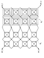
図7に、メッシュで接続された複数のホールセンサ素子11、12、…、44を含むホールセンサのもう1つの実施形態を示す。図6の実施形態と比較して、図7の(複数の)ホールセンサ素子は、45°回転されている。さらに、これらのホールセンサ素子のいくつかは、2つまたは4つの素子端子A、B、C、Dが一緒に接続されるように、隣接するホールセンサ素子に接続されている。たとえば、ホールセンサ素子21の素子端子Aは、その下隣りのホールセンサ素子22の素子端子B、左下隣りのホールセンサ素子12の素子端子C、および左隣りのホールセンサ素子11の素子端子Dに接続されている。同様の接続が、ホールセンサ素子22、23、31、32、33、41、42、43ならびにそのそれぞれの左隣り、左下隣り、および下隣りについても存在する。
FIG. 7 shows another embodiment of a Hall sensor including a plurality of
上記の実施形態のように、等分された第1の部分B1のホールセンサ素子の素子端子は、時計回りにラベル付けされ、等分された第2の部分B2のホールセンサ素子の素子端子は、反時計回りにラベル付けされ、それぞれ、左下角の素子端子Aから始まる。したがって、図7の配置も、対称性を有する。 As in the above embodiment, the element terminals of the hall sensor elements of the first part B 1 that are equally divided are labeled clockwise and the elements of the hall sensor elements of the second part B 2 that are equally divided. The terminals are labeled counterclockwise, each starting from the element terminal A in the lower left corner. Therefore, the arrangement of FIG. 7 also has symmetry.
この配置の端部のホールセンサ素子は、その隣りだけに接続される。図7のホールセンサは、ホールセンサ素子14の素子端子Aに接続されたセンサ端子EXT_A、ホールセンサ素子11の素子端子Bに接続されたセンサ端子EXT_B、ホールセンサ素子41の素子端子Cに接続されたセンサ端子EXT_C、ホールセンサ素子44の素子端子Dに接続されたセンサ端子EXT_Dを介して接続される。
The Hall sensor element at the end of this arrangement is connected only to its neighbor. 7 is connected to a sensor terminal EXT_A connected to the element terminal A of the
図6の実施形態と同様に、等分された第1および第2の部分B1、B2の位置での磁界の差に対応する差値を、2つのセンサ端子の間で測定することができる。 Similar to the embodiment of FIG. 6, a difference value corresponding to the difference in magnetic field at the position of the equally divided first and second parts B 1 , B 2 can be measured between the two sensor terminals. it can.
たとえば、メッシュ構成を有する実施形態の入力関連雑音BNoiseは、
Itot=IH+IFE
となる。
For example, the input related noise B Noise of the embodiment having a mesh configuration is
I tot = I H + I FE
It becomes.
上記の式では、抵抗RHは、センサ端子に現れる、接続されたホールセンサ素子の実効抵抗である。したがって、従来の手法と比較して半分の電流で、雑音は、√2倍に増加する。従来の手法と同じ雑音を得るために、電源電流または電源電圧を√2倍に増加させてよい。総電流Itotは、
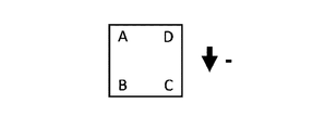
図8に、主にそれぞれの素子端子のラベリングが異なる、ホールセンサ素子のさまざまな可能な構成を示す。たとえば、図8A、図8B、図8C、および図8Dの構成は、それぞれの矢印の隣のプラス記号によって表される、素子端子が時計回りにラベル付けされる構成を示す。同様に、図8E、図8F、図8G、および図8Hは、それぞれの矢印の隣のマイナス記号によって表される、素子端子のラベリングが反時計回りに行われている構成を示す。 FIG. 8 shows various possible configurations of Hall sensor elements, mainly with different labeling of each element terminal. For example, the configurations of FIGS. 8A, 8B, 8C, and 8D show configurations in which element terminals are labeled clockwise, represented by a plus sign next to each arrow. Similarly, FIG. 8E, FIG. 8F, FIG. 8G, and FIG. 8H show configurations in which element terminals are labeled counterclockwise, represented by a minus sign next to each arrow.
矢印の向きは、ホールセンサ素子のどの角が、基準素子端子、たとえば素子端子Aがラベル付けされるのかを示す。具体的には、図8Aおよび図8Eで使用される右向き矢印は、左下角に素子端子Aのラベルが付けられることを示す。下向き矢印は、図8Bおよび図8Fに示されているように、左上角に素子端子Aのラベルが付けられることを示す。左向き矢印は、図8Cおよび図8Gに示されているように、右上角の素子端子Aのラベル付けを示す。最後に、上を指す矢印は、素子端子Aが、右下角に位置していることを示す。上記の実施形態のうちの1つによるホールセンサ内で、このさまざまな構成を、使用することができる。たとえば、上記のように、時計回りのラベリングを有する図8A、図8B、図8C、図8Cの構成を、等分された第1の部分B1内で使用してよく、反時計回りのラベリングを有する図8E、図8F、図8G、および図8Hの構成を、等分された第2の部分B2内で使用してよい。 The direction of the arrow indicates which corner of the Hall sensor element is labeled with a reference element terminal, eg element terminal A. Specifically, the right-pointing arrow used in FIGS. 8A and 8E indicates that the element terminal A is labeled at the lower left corner. The downward arrow indicates that the element terminal A is labeled at the upper left corner, as shown in FIGS. 8B and 8F. The left-pointing arrow indicates the labeling of element terminal A in the upper right corner, as shown in FIGS. 8C and 8G. Finally, the arrow pointing up indicates that the element terminal A is located at the lower right corner. This various configurations can be used in a Hall sensor according to one of the above embodiments. For example, as described above, the configurations of FIGS. 8A, 8B, 8C, and 8C having clockwise labeling may be used in the equally divided first portion B 1 and counterclockwise labeling. The configurations of FIGS. 8E, 8F, 8G, and 8H having the following may be used within the second divided portion B 2 .
図8に示されたそれぞれの構成を用いて、ホールセンサのさらなる実施形態を次に続く図に示す。それぞれの構成は、それぞれプラス記号またはマイナス記号を有するそれぞれの矢印として描かれる。 Using the respective configurations shown in FIG. 8, further embodiments of Hall sensors are shown in the following figures. Each configuration is depicted as a respective arrow with a plus or minus sign, respectively.
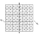
たとえば、図9に、8つのホールセンサ素子図8Aの構成に従って等分された左側半分B1内に設けられるホールセンサの実施形態を示す。このホールセンサの等分された右側半分B2では、左側半分B1に対して対称の配置で設けられる。この対称性は、右側半分B2のホールセンサ素子に図8Eの構成を適用することで生じる。個々のホールセンサ素子の間の相互接続は、たとえば図6または図7と同様に行われる。また、センサ端子EXT_A、EXT_B、EXT_C、EXT_Dを設けることは、たとえば図6または図7の実施形態のうちの1つに倣ってて行われてよい。 For example, FIG. 9 shows an embodiment of a Hall sensor provided in the left half B 1 equally divided into eight Hall sensor elements according to the configuration of FIG. 8A. The equally divided right half B 2 of the Hall sensor is provided in a symmetrical arrangement with respect to the left half B 1 . This symmetry results in applying the configuration of FIG. 8E to the Hall sensor element right half B 2. The interconnection between the individual Hall sensor elements is performed in the same way as in FIG. 6 or FIG. Also, providing the sensor terminals EXT_A, EXT_B, EXT_C, and EXT_D may be performed, for example, following one of the embodiments of FIG. 6 or FIG.
図9の実施形態では、使用されるホールセンサ素子は、基本的に同一の向きを有する。図10に、図9の実施形態と同様なホールセンサのさらなる実施形態を示し、ここでは、個々のホールセンサ素子が、互いに対して回転されているが、これは異なる向きの矢印でわかる。しかし、左側B1のホールセンサ素子が、プラス記号によって表されるように時計回りにラベル付けされ、右側B2のホールセンサ素子が、マイナス記号によって表されるように反時計回りにラベル付けされているので、等分された2つの部分B1、B2の間でそれぞれ対称性が与えられまたは保持されている。このように、この対称性のおかげで、上記の実施形態では、センサ端子で差値がもたらされる。 In the embodiment of FIG. 9, the Hall sensor elements used have basically the same orientation. FIG. 10 shows a further embodiment of a Hall sensor similar to the embodiment of FIG. 9, where the individual Hall sensor elements are rotated relative to each other, as can be seen by arrows of different orientations. However, the Hall sensor elements of the left B 1 is, labeled clockwise as represented by the plus sign, the Hall sensor elements of the right B 2 is labeled counterclockwise as represented by the minus sign Therefore, symmetry is given or maintained between the two equally divided parts B 1 and B 2 . Thus, thanks to this symmetry, the above embodiment provides a difference value at the sensor terminal.
図10の実施形態とは特に使用されるホールセンサ素子の個数が異なる、ホールセンサのさらなる実施形態を図11に示す。図11のホールセンサは、特に2つの半等分された部分B1、B2に分配された64個のホールセンサ素子を備える。図10の実施形態と同様に、個々のホールセンサ素子は、互いに対して回転されている。 FIG. 11 shows a further embodiment of the Hall sensor, which differs from the embodiment of FIG. 10 in that the number of Hall sensor elements used is different. The Hall sensor of FIG. 11 comprises 64 Hall sensor elements distributed in particular in two halved parts B 1 , B 2 . Similar to the embodiment of FIG. 10, the individual Hall sensor elements are rotated relative to each other.
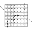
図12は、64個のホールセンサ素子を有するホールセンサのさらなる実施形態を示す。対称の線は、概ねこの配列体の対角線に沿ってホールセンサを分離している。しかし、前記の実施形態と同様に、それぞれのプラス記号またはマイナス記号によって示されるように、等分された第1の部分B1は、時計回りにラベル付けされたホールセンサ素子を備え、第2の部分B2は、反時計回りにラベル付けされたホールセンサ素子を備える。このように、この実施形態でも、等分された第1および第2の部分B1、B2の2つの位置での磁界強度の差に対応する差値が、図12のホールセンサによってもたらされ得る。 FIG. 12 shows a further embodiment of a Hall sensor having 64 Hall sensor elements. Symmetric lines separate the Hall sensors generally along the diagonal of the array. However, as in the previous embodiment, as indicated by the respective plus or minus sign, the equally divided first portion B 1 comprises a Hall sensor element labeled clockwise and a second Part B 2 of FIG. 4 includes Hall sensor elements labeled counterclockwise. Thus, also in this embodiment, a difference value corresponding to the difference in magnetic field strength at the two positions of the equally divided first and second portions B 1 and B 2 is provided by the Hall sensor of FIG. Can be done.
上記の実施形態のホールセンサを図1のセンサ配列体に適用する場合は、ホールセンサを動作させるために単一の増幅器および単一の電源回路またはバイアス回路だけが必要である。また、チョッピング装置またはデチョッピング(dechopping)装置が、ホールセンサ信号の評価のために使用される場合には、単一のチョッピング/デチョッピング回路だけが、このセンサ配列体のために必要である。したがって、従来の手法と比較して、必要な回路部品が少なく、電力消費が低減される。 When the Hall sensor of the above embodiment is applied to the sensor array of FIG. 1, only a single amplifier and a single power supply or bias circuit are required to operate the Hall sensor. Also, if a chopping device or dechopping device is used for the evaluation of the Hall sensor signal, only a single chopping / dechopping circuit is required for this sensor array. Therefore, compared with the conventional method, fewer circuit parts are required and power consumption is reduced.
逆並列構成の図3および図4の実施形態および、図6、図7、図9〜図12の実施形態では、センサ端子のうちの2つが電源信号を供給するのに使用され、センサ端子の他の2つが、差値をもたらすのに使用されることで、そのまま従来のホールセンサのように動作させることができる。したがって、従来のホールセンサと比較して、電流スピニングなどの技法を、変更なしで適用することができる。 In the embodiment of FIGS. 3 and 4 in an anti-parallel configuration and the embodiments of FIGS. 6, 7, and 9-12, two of the sensor terminals are used to provide a power signal, and the sensor terminals The other two are used to provide the difference value, so that it can be operated like a conventional Hall sensor as it is. Thus, techniques such as current spinning can be applied without modification compared to conventional Hall sensors.
しかし、図5の実施形態の逆直列構成を、上記で示したように、電源電流のそれぞれの変更によって電流スピニング技法を用いて動作させることもできる。 However, the anti-series configuration of the embodiment of FIG. 5 can also be operated using current spinning techniques with each change in power supply current, as indicated above.
ホールセンサのメッシュ状構成を用いると、たとえばセンサ端子に接続される素子端子の個数および位置を選択することによって、生じるホールセンサの抵抗を変更したり、影響を与えることができる。特に、ホールセンサの抵抗は、センサ端子に直接に接続されるホールセンサ素子の個数を増やすことによって低減することができる。 When the mesh configuration of the hall sensor is used, the resistance of the hall sensor to be generated can be changed or influenced by selecting the number and position of the element terminals connected to the sensor terminal, for example. In particular, the resistance of the Hall sensor can be reduced by increasing the number of Hall sensor elements that are directly connected to the sensor terminals.
Claims (19)
各々の前記ホールセンサ素子(11、12、…、44)は、当該ホールセンサ素子の素子端子(A、B、C、D)のうちの2つの間で、個々のセンサ値をもたらすように構成され、
前記少なくとも4つのホールセンサ素子(11、12、…、44)は、第1の部分(B1)と第2の部分(B2)とに分配され、差値が前記センサ端子(EXT_A、EXT_B、EXT_C、EXT_D)のうちの2つの間で、それぞれの個々のセンサ値から生じて、電気的に生成されるように接続され、
前記第1の部分(B1)の前記ホールセンサ素子は、前記メッシュの第1の部分で相互接続され、前記第2の部分(B2)の前記ホールセンサ素子は、前記メッシュの第2の部分で相互接続され、前記メッシュの第1の部分および第2の部分双方が相互接続されており、
前記第1の部分(B1)の前記個々のセンサ値が、前記差値の被減数を形成し、前記第2の部分(B2)の前記個々のセンサ値が、前記差値の減数を形成し、同一の強度および同一の方向の均一の磁界が、前記第1および第2の部分(B1、B2)の双方に印加された場合、前記被減数および前記減数は、互いに打ち消すようになっている、
ことを特徴とするホールセンサ(HS)。 At least four sensor terminals (11, 12,...) Interconnected with a two-dimensional or three-dimensional mesh and at least four sensor terminals (EXT_A, EXT_B, EXT_C, EXT_D) for connecting a hall sensor (HS). 44), and the element terminals (A, B, C, D) of the Hall sensor elements (11, 12,..., 44) are connected between the sensor terminals (EXT_A, EXT_B, EXT_C, EXT_D). Hall sensor (HS)
Each Hall sensor element (11, 12,..., 44) is configured to provide an individual sensor value between two of the element terminals (A, B, C, D) of the Hall sensor element. And
The at least four Hall sensor elements (11, 12,..., 44) are distributed to the first part (B 1 ) and the second part (B 2 ), and the difference value is the sensor terminal (EXT_A, EXT_B). , EXT_C, EXT_D) resulting from each individual sensor value and connected to be electrically generated,
The Hall sensor elements of the first part (B 1 ) are interconnected at a first part of the mesh, and the Hall sensor elements of the second part (B 2 ) are second of the mesh. Interconnected at portions, both the first and second portions of the mesh are interconnected;
The individual sensor values of the first part (B 1 ) form a divisor of the difference value, and the individual sensor values of the second part (B 2 ) form a subtraction of the difference value. However, when a uniform magnetic field with the same strength and the same direction is applied to both the first and second portions (B 1 , B 2 ), the subtracted number and the subtracted number cancel each other. ing,
Hall sensor (HS) characterized by this.
前記第2の部分(B2)の前記ホールセンサ素子は、当該ホールセンサが前記第2の部分(B2)の領域での磁界強度に対応する第2の値に寄与するように接続され、
前記第1の値は、前記差値に対して、前記第2の値の寄与と比較して反対の符号を有する寄与をもたらすことを特徴とする、
請求項1または2に記載のホールセンサ(HS)。 The Hall sensor element of the first part (B 1 ) is connected such that the Hall sensor contributes to a first value corresponding to the magnetic field strength in the region of the first part (B 1 );
The Hall sensor element of the second part (B 2 ) is connected such that the Hall sensor contributes to a second value corresponding to the magnetic field strength in the region of the second part (B 2 );
The first value provides a contribution to the difference value having an opposite sign compared to the contribution of the second value;
The hall sensor (HS) according to claim 1 or 2.
請求項1乃至4のいずれか1項に記載のホールセンサ(HS)。 The Hall sensor element of the first part (B 1 ) is disposed in a first adjacent region of the Hall sensor (HS), and the Hall sensor element of the second part (B 2 ) is the first sensor. It is arranged in a second adjacent region of the Hall sensor (HS) that does not overlap with an adjacent region,
The hall sensor (HS) according to any one of claims 1 to 4.
請求項5に記載のホールセンサ(HS)。 The first adjacent region and the second adjacent region have a similar shape and are spaced apart from each other,
The hall sensor (HS) according to claim 5.
請求項1乃至6のいずれか1項に記載のホールセンサ(HS)。 All of the Hall sensor elements (11, 12, ..., 44) are formed as lateral Hall sensor elements,
The hall sensor (HS) according to any one of claims 1 to 6.
請求項1乃至6のいずれか1項に記載のホールセンサ(HS)。 All of the Hall sensor elements (11, 12,..., 44) are formed as longitudinal Hall sensor elements,
The hall sensor (HS) according to any one of claims 1 to 6.
請求項1乃至8のいずれか1項に記載のホールセンサ(HS)。 All of the Hall sensor elements (11, 12,..., 44) are at least partially configured to have the same characteristics and / or to have the same geometric dimensions. ,
The hall sensor (HS) according to any one of claims 1 to 8.
請求項1乃至9のいずれか1項に記載のホールセンサ(HS)。 The difference values of the first and second parts (B 1 , B 2 ) are generated simultaneously with both the subtracted number of the difference value and the reduced number of the difference value,
The hall sensor (HS) according to any one of claims 1 to 9.
請求項1乃至10のいずれか1項に記載のホールセンサ(HS)。 All the Hall sensor elements (11, 12,..., 44) are provided on one common semiconductor substrate,
The hall sensor (HS) according to any one of claims 1 to 10.
請求項12に記載のセンサ配列体。 The Hall sensor (HS) including the bias circuit (BIAS), the amplifier (AMP), and all the Hall sensor elements (11, 12,..., 44) is provided on one common semiconductor substrate. It is characterized by
The sensor array according to claim 12.
請求項1乃至11のいずれか1項に記載のホールセンサ(HS)。 Each of the two parts (B 1 , B 2 ) has at least two Hall sensor elements (11, 12,..., 44),
The hall sensor (HS) according to any one of claims 1 to 11 .
請求項1乃至11、及び請求項14のいずれか1項に記載のホールセンサ(HS)。 The at least four Hall sensor elements (11, 12,..., 44) are distributed into a first part (B 1 ) and a second part (B 2 ) ,
The hall sensor (HS) according to any one of claims 1 to 11 and claim 14 .
請求項7に記載のホールセンサ(HS)。 The lateral Hall sensor element is formed as a Hall plate,
The hall sensor (HS) according to claim 7.
請求項9に記載のホールセンサ(HS)。 All the Hall sensor elements (11, 12,..., 44) are configured to have the same dimensions and the same electrical parameters,
The hall sensor (HS) according to claim 9.
請求項1乃至11、及び請求項14乃至17のいずれか1項に記載のホールセンサ(HS)。 The difference value is electrically generated between two of the sensor terminals (EXT_A, EXT_B, EXT_C, EXT_D), whereas a power signal is provided to the other two of the sensor terminals; It is characterized by
The hall sensor (HS) according to any one of claims 1 to 11 and claims 14 to 17 .
請求項1乃至11、及び請求項14乃至18のいずれか1項に記載のホールセンサ(HS)。 The difference value is evaluated between the two of the sensor terminals (EXT_A, EXT_B, EXT_C, EXT_D) and is generated electrically so that it can be directly amplified by a single amplification stage. Features
The hall sensor (HS) according to any one of claims 1 to 11 and claims 14 to 18 .
Applications Claiming Priority (2)
| Application Number | Priority Date | Filing Date | Title |
|---|---|---|---|
| EP12153493.7 | 2012-02-01 | ||
| EP12153493.7A EP2624001B1 (en) | 2012-02-01 | 2012-02-01 | Hall sensor and sensor arrangement |
Related Parent Applications (1)
| Application Number | Title | Priority Date | Filing Date |
|---|---|---|---|
| JP2014555100A Division JP5997295B2 (en) | 2012-02-01 | 2012-11-13 | Hall sensor and sensor array |
Publications (2)
| Publication Number | Publication Date |
|---|---|
| JP2016194527A JP2016194527A (en) | 2016-11-17 |
| JP6431004B2 true JP6431004B2 (en) | 2018-11-28 |
Family
ID=47172636
Family Applications (2)
| Application Number | Title | Priority Date | Filing Date |
|---|---|---|---|
| JP2014555100A Expired - Fee Related JP5997295B2 (en) | 2012-02-01 | 2012-11-13 | Hall sensor and sensor array |
| JP2016132964A Expired - Fee Related JP6431004B2 (en) | 2012-02-01 | 2016-07-05 | Hall sensor and sensor array |
Family Applications Before (1)
| Application Number | Title | Priority Date | Filing Date |
|---|---|---|---|
| JP2014555100A Expired - Fee Related JP5997295B2 (en) | 2012-02-01 | 2012-11-13 | Hall sensor and sensor array |
Country Status (5)
| Country | Link |
|---|---|
| US (1) | US10042010B2 (en) |
| EP (1) | EP2624001B1 (en) |
| JP (2) | JP5997295B2 (en) |
| CN (1) | CN104285158B (en) |
| WO (1) | WO2013113418A1 (en) |
Families Citing this family (13)
| Publication number | Priority date | Publication date | Assignee | Title |
|---|---|---|---|---|
| EP2624001B1 (en) * | 2012-02-01 | 2015-01-07 | ams AG | Hall sensor and sensor arrangement |
| EP2778704B1 (en) | 2013-03-11 | 2015-09-16 | Ams Ag | Magnetic field sensor system |
| CN105209860B (en) * | 2013-05-22 | 2017-08-25 | 斯凯孚公司 | Sensor cluster used in sensor bearing |
| KR102174724B1 (en) * | 2014-04-30 | 2020-11-06 | 주식회사 해치텍 | Sensing system using plural group of hall sensors and apparatus using thereof |
| JP6618370B2 (en) * | 2015-03-05 | 2019-12-11 | エイブリック株式会社 | Magnetic sensor circuit |
| EP3118640B1 (en) | 2015-07-13 | 2021-06-23 | ams AG | Hall sensor |
| EP3312567B1 (en) * | 2016-10-18 | 2019-12-04 | ams AG | Rotary sensor arrangement and method for determining a failure status of such arrangement |
| CN106646316B (en) * | 2017-01-24 | 2019-06-14 | 上海麦歌恩微电子股份有限公司 | The test method of Hall switch sensor noise |
| JP6841692B2 (en) * | 2017-03-13 | 2021-03-10 | エイブリック株式会社 | Magnetic sensor circuit |
| US10534045B2 (en) | 2017-09-20 | 2020-01-14 | Texas Instruments Incorporated | Vertical hall-effect sensor for detecting two-dimensional in-plane magnetic fields |
| JP6436265B1 (en) * | 2018-04-04 | 2018-12-12 | 大日本印刷株式会社 | Protective film, method for preventing electrolyte from adhering around electrolyte inlet, and battery manufacturing method |
| US11163019B1 (en) * | 2020-08-05 | 2021-11-02 | Allegro Microsystems, Llc | Magnetic field sensors having stray field rejection |
| CN114089238A (en) * | 2021-12-15 | 2022-02-25 | 鑫雁电子科技(上海)有限公司 | Hall signal processing circuit |
Family Cites Families (36)
| Publication number | Priority date | Publication date | Assignee | Title |
|---|---|---|---|---|
| US2942177A (en) | 1955-05-06 | 1960-06-21 | Siemens Ag | Method and means for measuring magnetic field strength |
| GB822210A (en) | 1957-03-29 | 1959-10-21 | Gen Electric Co Ltd | Improvements in or relating to instruments for making magnetic measurements |
| US2987669A (en) | 1959-01-19 | 1961-06-06 | Gulton Ind Inc | Hall effect electromechanical sensing device |
| DE1194971B (en) | 1963-04-25 | 1965-06-16 | Siemens Ag | Magnetic field measuring probe with Hall generator |
| JPS4980130U (en) * | 1972-10-28 | 1974-07-11 | ||
| JPS5748265A (en) * | 1980-08-29 | 1982-03-19 | Rohm Co Ltd | Magnetic coupler |
| JPS58154263A (en) | 1982-03-09 | 1983-09-13 | Seiko Instr & Electronics Ltd | Hall IC |
| US4737710A (en) * | 1983-01-27 | 1988-04-12 | Trw Inc. | Hall-effect array for sensing second spatial derivative of magnetic field |
| DE3435455A1 (en) * | 1984-09-27 | 1986-03-27 | Nukem Gmbh, 6450 Hanau | DEVICE WITH TWO HALL GENERATORS FOR MEASURING THE GRADIENT MAGNETIC FIELDS |
| EP0363512B1 (en) | 1988-10-13 | 1992-05-06 | Siemens Aktiengesellschaft | Non-contacting arrangement for the speed detection of a toothed wheel |
| US5241270A (en) | 1990-04-02 | 1993-08-31 | Kim Kwee Ng | Electronic compass using hall-effect sensors |
| EP0548391B1 (en) | 1991-12-21 | 1997-07-23 | Deutsche ITT Industries GmbH | Offset compensated Hall-sensor |
| DE4422868C2 (en) | 1994-06-30 | 1997-08-21 | Itt Ind Gmbh Deutsche | Device for determining an angle of rotation of a magnet |
| EP0793075B1 (en) | 1996-03-02 | 2002-09-25 | Micronas GmbH | Monolithic integrated sensor circuit |
| DE19943128A1 (en) * | 1999-09-09 | 2001-04-12 | Fraunhofer Ges Forschung | Hall sensor arrangement for offset-compensated magnetic field measurement |
| DE10150955C1 (en) | 2001-10-16 | 2003-06-12 | Fraunhofer Ges Forschung | Vertical Hall sensor |
| NL1024114C1 (en) | 2003-08-15 | 2005-02-16 | Systematic Design Holding B V | Method and device for taking measurements on magnetic fields using a hall sensor. |
| JP4698959B2 (en) * | 2004-03-05 | 2011-06-08 | 東北電力株式会社 | Sensor for detecting conductor defects in electric wires |
| JP4798102B2 (en) | 2004-03-30 | 2011-10-19 | 株式会社デンソー | Vertical Hall element |
| DE102005014509B4 (en) * | 2005-03-30 | 2007-09-13 | Austriamicrosystems Ag | Sensor arrangement and method for determining a rotation angle |
| US7902820B2 (en) * | 2005-05-03 | 2011-03-08 | Imec | Method and apparatus for detecting spatially varying and time-dependent magnetic fields |
| DE102006037226B4 (en) * | 2006-08-09 | 2008-05-29 | Fraunhofer-Gesellschaft zur Förderung der angewandten Forschung e.V. | Calibratable magnetic 3D-point sensor during measuring operation |
| WO2008054056A1 (en) * | 2006-11-01 | 2008-05-08 | Industry-Academic Cooperation Foundation, Chosun University | Magnetic sensor array and apparatus for detecting defect using the magnetic sensor array |
| EP2115467A1 (en) * | 2007-02-23 | 2009-11-11 | Koninklijke Philips Electronics N.V. | Magnetic sensor device with field generator and sensor element |
| CN101802631B (en) * | 2007-09-10 | 2014-10-22 | Ntn株式会社 | sensor assembly |
| GB0724240D0 (en) | 2007-12-12 | 2008-01-30 | Melexis Nv | Twin vertical hall sensor |
| DE102008000943B4 (en) * | 2008-04-02 | 2015-02-19 | Zf Friedrichshafen Ag | Diagnostic Hall sensor and method for functional diagnosis of a Hall sensor device |
| CN201628764U (en) * | 2010-01-30 | 2010-11-10 | 大连恒森微波电子有限公司 | Hall effect integrated sensor |
| US8760149B2 (en) | 2010-04-08 | 2014-06-24 | Infineon Technologies Ag | Magnetic field current sensors |
| JP5609326B2 (en) | 2010-07-01 | 2014-10-22 | 富士通セミコンダクター株式会社 | Clock divider circuit |
| DE102011017096A1 (en) | 2011-04-14 | 2012-10-18 | Austriamicrosystems Ag | Hall sensor semiconductor device and method of operating the Hall sensor semiconductor device |
| US9007060B2 (en) * | 2011-07-21 | 2015-04-14 | Infineon Technologies Ag | Electronic device with ring-connected hall effect regions |
| DE102011115566A1 (en) * | 2011-10-10 | 2013-04-11 | Austriamicrosystems Ag | Hall sensor |
| US8922207B2 (en) * | 2011-11-17 | 2014-12-30 | Infineon Technologies Ag | Electronic device comprising hall effect region with three contacts |
| EP2624001B1 (en) * | 2012-02-01 | 2015-01-07 | ams AG | Hall sensor and sensor arrangement |
| EP2682762A1 (en) * | 2012-07-06 | 2014-01-08 | Senis AG | Current transducer for measuring an electrical current, magnetic transducer and current leakage detection system and method |
-
2012
- 2012-02-01 EP EP12153493.7A patent/EP2624001B1/en not_active Revoked
- 2012-11-13 CN CN201280068703.7A patent/CN104285158B/en not_active Expired - Fee Related
- 2012-11-13 US US14/374,521 patent/US10042010B2/en active Active
- 2012-11-13 JP JP2014555100A patent/JP5997295B2/en not_active Expired - Fee Related
- 2012-11-13 WO PCT/EP2012/072503 patent/WO2013113418A1/en not_active Ceased
-
2016
- 2016-07-05 JP JP2016132964A patent/JP6431004B2/en not_active Expired - Fee Related
Also Published As
| Publication number | Publication date |
|---|---|
| JP5997295B2 (en) | 2016-09-28 |
| JP2015507192A (en) | 2015-03-05 |
| EP2624001A1 (en) | 2013-08-07 |
| US20140361766A1 (en) | 2014-12-11 |
| US10042010B2 (en) | 2018-08-07 |
| CN104285158B (en) | 2017-02-22 |
| EP2624001B1 (en) | 2015-01-07 |
| JP2016194527A (en) | 2016-11-17 |
| WO2013113418A1 (en) | 2013-08-08 |
| CN104285158A (en) | 2015-01-14 |
Similar Documents
| Publication | Publication Date | Title |
|---|---|---|
| JP6431004B2 (en) | Hall sensor and sensor array | |
| JP5969613B2 (en) | Hall sensor | |
| US9063187B2 (en) | Hall sensor element and method for measuring a magnetic field | |
| JP6474822B2 (en) | High sensitivity push-pull bridge magnetic sensor | |
| US10024930B2 (en) | Single chip referenced bridge magnetic sensor for high-intensity magnetic field | |
| CN105143903B (en) | Magnetic field sensor system | |
| TWI452319B (en) | Magnetoresistive sensing device | |
| US10312286B2 (en) | Magnetic sensor including resistor array including a plurality of resistive element sections each having magnetoresistance element | |
| KR101755698B1 (en) | Hall sensor | |
| KR102533697B1 (en) | magnetic field sensor | |
| JP2017502298A5 (en) | ||
| CN106164691B (en) | Low offset and high sensitivity vertical hall effect sensor | |
| US9651635B2 (en) | Bias circuit for stacked hall devices | |
| US11119160B2 (en) | Hall sensor, corresponding devices and method | |
| JP2004077374A (en) | Arranging structure of magnetic sensor | |
| US9851419B2 (en) | Hall sensor | |
| JP2013201229A (en) | Hall sensor | |
| JP2019219293A (en) | Magnetic sensor | |
| CN121442957B (en) | Two-Differential 2D Hall Integrated Chip and Its Design Method | |
| US20250298097A1 (en) | Gmr layout for compact transducer with mismatch control | |
| JP2024157700A (en) | Magnetic Sensors | |
| Krasyukov et al. | Investigation of magnetotransistors with new topology | |
| UA73816C2 (en) | Magnetic field strength transducer |
Legal Events
| Date | Code | Title | Description |
|---|---|---|---|
| A977 | Report on retrieval |
Free format text: JAPANESE INTERMEDIATE CODE: A971007 Effective date: 20170413 |
|
| A131 | Notification of reasons for refusal |
Free format text: JAPANESE INTERMEDIATE CODE: A131 Effective date: 20170607 |
|
| A601 | Written request for extension of time |
Free format text: JAPANESE INTERMEDIATE CODE: A601 Effective date: 20170906 |
|
| A521 | Request for written amendment filed |
Free format text: JAPANESE INTERMEDIATE CODE: A523 Effective date: 20170922 |
|
| A131 | Notification of reasons for refusal |
Free format text: JAPANESE INTERMEDIATE CODE: A131 Effective date: 20180307 |
|
| A521 | Request for written amendment filed |
Free format text: JAPANESE INTERMEDIATE CODE: A523 Effective date: 20180511 |
|
| TRDD | Decision of grant or rejection written | ||
| A01 | Written decision to grant a patent or to grant a registration (utility model) |
Free format text: JAPANESE INTERMEDIATE CODE: A01 Effective date: 20181003 |
|
| A61 | First payment of annual fees (during grant procedure) |
Free format text: JAPANESE INTERMEDIATE CODE: A61 Effective date: 20181101 |
|
| R150 | Certificate of patent or registration of utility model |
Ref document number: 6431004 Country of ref document: JP Free format text: JAPANESE INTERMEDIATE CODE: R150 |
|
| R250 | Receipt of annual fees |
Free format text: JAPANESE INTERMEDIATE CODE: R250 |
|
| LAPS | Cancellation because of no payment of annual fees |