JP6447166B2 - 化合物半導体装置及びその製造方法 - Google Patents
化合物半導体装置及びその製造方法 Download PDFInfo
- Publication number
- JP6447166B2 JP6447166B2 JP2015010723A JP2015010723A JP6447166B2 JP 6447166 B2 JP6447166 B2 JP 6447166B2 JP 2015010723 A JP2015010723 A JP 2015010723A JP 2015010723 A JP2015010723 A JP 2015010723A JP 6447166 B2 JP6447166 B2 JP 6447166B2
- Authority
- JP
- Japan
- Prior art keywords
- layer
- region
- barrier layer
- semiconductor device
- substrate
- Prior art date
- Legal status (The legal status is an assumption and is not a legal conclusion. Google has not performed a legal analysis and makes no representation as to the accuracy of the status listed.)
- Expired - Fee Related
Links
Images


Classifications
-
- H—ELECTRICITY
- H10—SEMICONDUCTOR DEVICES; ELECTRIC SOLID-STATE DEVICES NOT OTHERWISE PROVIDED FOR
- H10D—INORGANIC ELECTRIC SEMICONDUCTOR DEVICES
- H10D62/00—Semiconductor bodies, or regions thereof, of devices having potential barriers
- H10D62/40—Crystalline structures
- H10D62/405—Orientations of crystalline planes
-
- H—ELECTRICITY
- H10—SEMICONDUCTOR DEVICES; ELECTRIC SOLID-STATE DEVICES NOT OTHERWISE PROVIDED FOR
- H10D—INORGANIC ELECTRIC SEMICONDUCTOR DEVICES
- H10D30/00—Field-effect transistors [FET]
- H10D30/40—FETs having zero-dimensional [0D], one-dimensional [1D] or two-dimensional [2D] charge carrier gas channels
- H10D30/47—FETs having zero-dimensional [0D], one-dimensional [1D] or two-dimensional [2D] charge carrier gas channels having two-dimensional [2D] charge carrier gas channels, e.g. nanoribbon FETs or high electron mobility transistors [HEMT]
- H10D30/471—High electron mobility transistors [HEMT] or high hole mobility transistors [HHMT]
- H10D30/475—High electron mobility transistors [HEMT] or high hole mobility transistors [HHMT] having wider bandgap layer formed on top of lower bandgap active layer, e.g. undoped barrier HEMTs such as i-AlGaN/GaN HEMTs
-
- H—ELECTRICITY
- H10—SEMICONDUCTOR DEVICES; ELECTRIC SOLID-STATE DEVICES NOT OTHERWISE PROVIDED FOR
- H10D—INORGANIC ELECTRIC SEMICONDUCTOR DEVICES
- H10D62/00—Semiconductor bodies, or regions thereof, of devices having potential barriers
- H10D62/10—Shapes, relative sizes or dispositions of the regions of the semiconductor bodies; Shapes of the semiconductor bodies
- H10D62/113—Isolations within a component, i.e. internal isolations
- H10D62/115—Dielectric isolations, e.g. air gaps
-
- H—ELECTRICITY
- H10—SEMICONDUCTOR DEVICES; ELECTRIC SOLID-STATE DEVICES NOT OTHERWISE PROVIDED FOR
- H10D—INORGANIC ELECTRIC SEMICONDUCTOR DEVICES
- H10D62/00—Semiconductor bodies, or regions thereof, of devices having potential barriers
- H10D62/80—Semiconductor bodies, or regions thereof, of devices having potential barriers characterised by the materials
- H10D62/82—Heterojunctions
- H10D62/824—Heterojunctions comprising only Group III-V materials heterojunctions, e.g. GaN/AlGaN heterojunctions
-
- H—ELECTRICITY
- H10—SEMICONDUCTOR DEVICES; ELECTRIC SOLID-STATE DEVICES NOT OTHERWISE PROVIDED FOR
- H10D—INORGANIC ELECTRIC SEMICONDUCTOR DEVICES
- H10D8/00—Diodes
- H10D8/01—Manufacture or treatment
- H10D8/053—Manufacture or treatment of heterojunction diodes or of tunnel diodes
-
- H—ELECTRICITY
- H10—SEMICONDUCTOR DEVICES; ELECTRIC SOLID-STATE DEVICES NOT OTHERWISE PROVIDED FOR
- H10D—INORGANIC ELECTRIC SEMICONDUCTOR DEVICES
- H10D8/00—Diodes
- H10D8/70—Tunnel-effect diodes
- H10D8/755—Resonant tunneling diodes [RTD]
-
- H—ELECTRICITY
- H10—SEMICONDUCTOR DEVICES; ELECTRIC SOLID-STATE DEVICES NOT OTHERWISE PROVIDED FOR
- H10D—INORGANIC ELECTRIC SEMICONDUCTOR DEVICES
- H10D84/00—Integrated devices formed in or on semiconductor substrates that comprise only semiconducting layers, e.g. on Si wafers or on GaAs-on-Si wafers
- H10D84/01—Manufacture or treatment
- H10D84/0107—Integrating at least one component covered by H10D12/00 or H10D30/00 with at least one component covered by H10D8/00, H10D10/00 or H10D18/00, e.g. integrating IGFETs with BJTs
-
- H—ELECTRICITY
- H10—SEMICONDUCTOR DEVICES; ELECTRIC SOLID-STATE DEVICES NOT OTHERWISE PROVIDED FOR
- H10D—INORGANIC ELECTRIC SEMICONDUCTOR DEVICES
- H10D84/00—Integrated devices formed in or on semiconductor substrates that comprise only semiconducting layers, e.g. on Si wafers or on GaAs-on-Si wafers
- H10D84/01—Manufacture or treatment
- H10D84/02—Manufacture or treatment characterised by using material-based technologies
- H10D84/05—Manufacture or treatment characterised by using material-based technologies using Group III-V technology
-
- H—ELECTRICITY
- H10—SEMICONDUCTOR DEVICES; ELECTRIC SOLID-STATE DEVICES NOT OTHERWISE PROVIDED FOR
- H10D—INORGANIC ELECTRIC SEMICONDUCTOR DEVICES
- H10D84/00—Integrated devices formed in or on semiconductor substrates that comprise only semiconducting layers, e.g. on Si wafers or on GaAs-on-Si wafers
- H10D84/80—Integrated devices formed in or on semiconductor substrates that comprise only semiconducting layers, e.g. on Si wafers or on GaAs-on-Si wafers characterised by the integration of at least one component covered by groups H10D12/00 or H10D30/00, e.g. integration of IGFETs
- H10D84/811—Combinations of field-effect devices and one or more diodes, capacitors or resistors
-
- H—ELECTRICITY
- H10—SEMICONDUCTOR DEVICES; ELECTRIC SOLID-STATE DEVICES NOT OTHERWISE PROVIDED FOR
- H10P—GENERIC PROCESSES OR APPARATUS FOR THE MANUFACTURE OR TREATMENT OF DEVICES COVERED BY CLASS H10
- H10P14/00—Formation of materials, e.g. in the shape of layers or pillars
- H10P14/20—Formation of materials, e.g. in the shape of layers or pillars of semiconductor materials
- H10P14/34—Deposited materials, e.g. layers
- H10P14/3466—Crystal orientation
-
- H—ELECTRICITY
- H10—SEMICONDUCTOR DEVICES; ELECTRIC SOLID-STATE DEVICES NOT OTHERWISE PROVIDED FOR
- H10D—INORGANIC ELECTRIC SEMICONDUCTOR DEVICES
- H10D62/00—Semiconductor bodies, or regions thereof, of devices having potential barriers
- H10D62/80—Semiconductor bodies, or regions thereof, of devices having potential barriers characterised by the materials
- H10D62/81—Semiconductor bodies, or regions thereof, of devices having potential barriers characterised by the materials of structures exhibiting quantum-confinement effects, e.g. single quantum wells; of structures having periodic or quasi-periodic potential variation
- H10D62/815—Semiconductor bodies, or regions thereof, of devices having potential barriers characterised by the materials of structures exhibiting quantum-confinement effects, e.g. single quantum wells; of structures having periodic or quasi-periodic potential variation of structures having periodic or quasi-periodic potential variation, e.g. superlattices or multiple quantum wells [MQW]
- H10D62/8161—Semiconductor bodies, or regions thereof, of devices having potential barriers characterised by the materials of structures exhibiting quantum-confinement effects, e.g. single quantum wells; of structures having periodic or quasi-periodic potential variation of structures having periodic or quasi-periodic potential variation, e.g. superlattices or multiple quantum wells [MQW] potential variation due to variations in composition or crystallinity, e.g. heterojunction superlattices
- H10D62/8162—Semiconductor bodies, or regions thereof, of devices having potential barriers characterised by the materials of structures exhibiting quantum-confinement effects, e.g. single quantum wells; of structures having periodic or quasi-periodic potential variation of structures having periodic or quasi-periodic potential variation, e.g. superlattices or multiple quantum wells [MQW] potential variation due to variations in composition or crystallinity, e.g. heterojunction superlattices having quantum effects only in the vertical direction, i.e. layered structures having quantum effects solely resulting from vertical potential variation
- H10D62/8164—Semiconductor bodies, or regions thereof, of devices having potential barriers characterised by the materials of structures exhibiting quantum-confinement effects, e.g. single quantum wells; of structures having periodic or quasi-periodic potential variation of structures having periodic or quasi-periodic potential variation, e.g. superlattices or multiple quantum wells [MQW] potential variation due to variations in composition or crystallinity, e.g. heterojunction superlattices having quantum effects only in the vertical direction, i.e. layered structures having quantum effects solely resulting from vertical potential variation comprising only semiconductor materials
-
- H—ELECTRICITY
- H10—SEMICONDUCTOR DEVICES; ELECTRIC SOLID-STATE DEVICES NOT OTHERWISE PROVIDED FOR
- H10D—INORGANIC ELECTRIC SEMICONDUCTOR DEVICES
- H10D62/00—Semiconductor bodies, or regions thereof, of devices having potential barriers
- H10D62/80—Semiconductor bodies, or regions thereof, of devices having potential barriers characterised by the materials
- H10D62/85—Semiconductor bodies, or regions thereof, of devices having potential barriers characterised by the materials being Group III-V materials, e.g. GaAs
- H10D62/8503—Nitride Group III-V materials, e.g. AlN or GaN
-
- H—ELECTRICITY
- H10—SEMICONDUCTOR DEVICES; ELECTRIC SOLID-STATE DEVICES NOT OTHERWISE PROVIDED FOR
- H10D—INORGANIC ELECTRIC SEMICONDUCTOR DEVICES
- H10D64/00—Electrodes of devices having potential barriers
- H10D64/60—Electrodes characterised by their materials
- H10D64/602—Heterojunction gate electrodes for FETs
-
- H—ELECTRICITY
- H10—SEMICONDUCTOR DEVICES; ELECTRIC SOLID-STATE DEVICES NOT OTHERWISE PROVIDED FOR
- H10D—INORGANIC ELECTRIC SEMICONDUCTOR DEVICES
- H10D84/00—Integrated devices formed in or on semiconductor substrates that comprise only semiconducting layers, e.g. on Si wafers or on GaAs-on-Si wafers
- H10D84/40—Integrated devices formed in or on semiconductor substrates that comprise only semiconducting layers, e.g. on Si wafers or on GaAs-on-Si wafers characterised by the integration of at least one component covered by groups H10D12/00 or H10D30/00 with at least one component covered by groups H10D10/00 or H10D18/00, e.g. integration of IGFETs with BJTs
- H10D84/401—Combinations of FETs or IGBTs with BJTs
-
- H—ELECTRICITY
- H10—SEMICONDUCTOR DEVICES; ELECTRIC SOLID-STATE DEVICES NOT OTHERWISE PROVIDED FOR
- H10P—GENERIC PROCESSES OR APPARATUS FOR THE MANUFACTURE OR TREATMENT OF DEVICES COVERED BY CLASS H10
- H10P14/00—Formation of materials, e.g. in the shape of layers or pillars
- H10P14/20—Formation of materials, e.g. in the shape of layers or pillars of semiconductor materials
- H10P14/32—Formation of materials, e.g. in the shape of layers or pillars of semiconductor materials characterised by intermediate layers between substrates and deposited layers
- H10P14/3202—Materials thereof
- H10P14/3214—Materials thereof being Group IIIA-VA semiconductors
- H10P14/3216—Nitrides
-
- H—ELECTRICITY
- H10—SEMICONDUCTOR DEVICES; ELECTRIC SOLID-STATE DEVICES NOT OTHERWISE PROVIDED FOR
- H10P—GENERIC PROCESSES OR APPARATUS FOR THE MANUFACTURE OR TREATMENT OF DEVICES COVERED BY CLASS H10
- H10P14/00—Formation of materials, e.g. in the shape of layers or pillars
- H10P14/20—Formation of materials, e.g. in the shape of layers or pillars of semiconductor materials
- H10P14/34—Deposited materials, e.g. layers
- H10P14/3402—Deposited materials, e.g. layers characterised by the chemical composition
- H10P14/3414—Deposited materials, e.g. layers characterised by the chemical composition being group IIIA-VIA materials
- H10P14/3416—Nitrides
-
- H—ELECTRICITY
- H10—SEMICONDUCTOR DEVICES; ELECTRIC SOLID-STATE DEVICES NOT OTHERWISE PROVIDED FOR
- H10W—GENERIC PACKAGES, INTERCONNECTIONS, CONNECTORS OR OTHER CONSTRUCTIONAL DETAILS OF DEVICES COVERED BY CLASS H10
- H10W74/00—Encapsulations, e.g. protective coatings
- H10W74/10—Encapsulations, e.g. protective coatings characterised by their shape or disposition
- H10W74/131—Encapsulations, e.g. protective coatings characterised by their shape or disposition the semiconductor body being only partially enclosed
- H10W74/137—Encapsulations, e.g. protective coatings characterised by their shape or disposition the semiconductor body being only partially enclosed the encapsulations being directly on the semiconductor body
Landscapes
- Metal-Oxide And Bipolar Metal-Oxide Semiconductor Integrated Circuits (AREA)
- Junction Field-Effect Transistors (AREA)
- Bipolar Transistors (AREA)
- Chemical & Material Sciences (AREA)
- Crystallography & Structural Chemistry (AREA)
Description
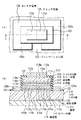
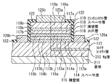
先ず、第1の実施形態について説明する。第1の実施形態は、共鳴トンネルダイオード(RTD)を備えた化合物半導体装置に関する。図1は、第1の実施形態に係る化合物半導体装置の構成を示す図である。図1(a)は平面図であり、図1(b)は図1(a)中のI−I線に沿った断面図である。
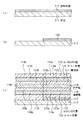
次に、第2の実施形態について説明する。図5は、第2の実施形態に係る化合物半導体装置の構成を示す断面図である。
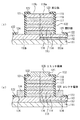
次に、第3の実施形態について説明する。図6は、第3の実施形態に係る化合物半導体装置の構成を示す断面図である。
次に、第4の実施形態について説明する。図7は、第4の実施形態に係る化合物半導体装置の構成を示す断面図である。
次に、第5の実施形態について説明する。第5の実施形態は、共鳴トンネルダイオード(RTD)及び高電子移動度トランジスタ(HEMT)を備えた化合物半導体装置の一例である。図8Aは、第5の実施形態に係る化合物半導体装置の構成を示す平面図であり、図8Bは、図8A中のI−I線に沿った断面図である。
次に、第6の実施形態について説明する。第6の実施形態は、共鳴トンネルダイオード(RTD)及び高電子移動度トランジスタ(HEMT)を備えた化合物半導体装置の一例である。図10は、第6の実施形態に係る化合物半導体装置の構成を示す断面図である。
次に、第7の実施形態について説明する。第7の実施形態は、高速論理ゲートMOBILE回路の一例である。図11は、第7の実施形態に係る論理回路の構成を示す結線図である。
次に、第8の実施形態について説明する。第8の実施形態は、発振器の一例である。図12は、第8の実施形態に係る発振器の構成を示す結線図である。
次に、第9の実施形態について説明する。第9の実施形態は、イメージングセンサの一例である。図13は、第9の実施形態に係るセンサの構成を示す結線図である。
基板と、
前記基板上方の窒化物半導体の第1の障壁層、前記第1の障壁層上の窒化物半導体の井戸層、前記井戸層上の窒化物半導体の第2の障壁層を含む共鳴トンネルダイオードと、
を有し、
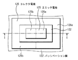
前記第1の障壁層、前記井戸層及び前記第2の障壁層の各々が、上面が(0001)面の第1の領域及び上面が(000−1)面の第2の領域を有し、
前記第1の障壁層、前記井戸層及び前記第2の障壁層の間で、前記第1の領域同士が前記基板の厚さ方向で積層され、前記第2の領域同士が前記基板の厚さ方向で積層され、
前記第1の領域同士が積層された部分に第1のエミッタ電極及び第1のコレクタ電極が設けられ、
前記第2の領域同士が積層された部分に第2のエミッタ電極及び第2のコレクタ電極が設けられ、
前記第1のエミッタ電極と前記第2のエミッタ電極とが電気的に互いに接続され、
前記第1のコレクタ電極と前記第2のコレクタ電極とが電気的に互いに接続されていることを特徴とする化合物半導体装置。
前記第1の障壁層及び前記第2の障壁層がInxAlyGa1-x-yN(0≦x<1、0≦y<1、0<x+y<1)層を含み、
前記井戸層がInzGa1-zN(0≦z<1)層を含むことを特徴とする付記1に記載の化合物半導体装置。
前記第1の障壁層、前記井戸層及び前記第2の障壁層の各々において、前記第1の領域と前記第2の領域との境界にイオン注入領域が形成されていることを特徴とする付記1又は2に記載の化合物半導体装置。
前記第1の障壁層、前記井戸層及び前記第2の障壁層の各々において、前記第1の領域と前記第2の領域との境界にパッシベーション膜が形成されていることを特徴とする付記1又は2に記載の化合物半導体装置。
前記基板がサファイア基板、炭化シリコン基板、窒化ガリウム基板又は窒化アルミニウム基板であることを特徴とする付記1乃至4のいずれか1項に記載の化合物半導体装置。
前記第1のエミッタ電極と前記第2のエミッタ電極とが一体化され、
前記第1のコレクタ電極と前記第2のコレクタ電極とが一体化されていることを特徴とする付記1乃至5のいずれか1項に記載の化合物半導体装置。
前記基板上に形成された高電子移動度トランジスタを有することを特徴とする付記1乃至6のいずれか1項に記載の化合物半導体装置。
付記1乃至6のいずれか1項に記載の化合物半導体装置を有することを特徴とする論理回路。
付記1乃至6のいずれか1項に記載の化合物半導体装置を有することを特徴とする発振器。
付記1乃至6のいずれか1項に記載の化合物半導体装置を有することを特徴とするセンサ。
基板上方に、窒化物半導体の第1の障壁層、前記第1の障壁層上の窒化物半導体の井戸層、前記井戸層上の窒化物半導体の第2の障壁層を含む共鳴トンネルダイオードを形成する工程を有し、
前記第1の障壁層、前記井戸層及び前記第2の障壁層の各々が、上面が(0001)面の第1の領域及び上面が(000−1)面の第2の領域を有し、
前記第1の障壁層、前記井戸層及び前記第2の障壁層の間で、前記第1の領域同士が前記基板の厚さ方向で積層され、前記第2の領域同士が前記基板の厚さ方向で積層され、
前記第1の領域同士が積層された部分に第1のエミッタ電極及び第1のコレクタ電極を形成する工程と、
前記第2の領域同士が積層された部分に第2のエミッタ電極及び第2のコレクタ電極を形成する工程と、
を有し、
前記第1のエミッタ電極と前記第2のエミッタ電極とが電気的に互いに接続され、
前記第1のコレクタ電極と前記第2のコレクタ電極とが電気的に互いに接続されていることを特徴とする化合物半導体装置の製造方法。
前記第1の障壁層及び前記第2の障壁層がInxAlyGa1-x-yN(0≦x<1、0≦y<1、0<x+y<1)層を含み、
前記井戸層がInzGa1-zN(0≦z<1)層を含むことを特徴とする付記11に記載の化合物半導体装置の製造方法。
前記第1の障壁層、前記井戸層及び前記第2の障壁層の各々において、前記第1の領域と前記第2の領域との境界にイオン注入を行う工程を有することを特徴とする付記11又は12に記載の化合物半導体装置の製造方法。
前記第1の障壁層、前記井戸層及び前記第2の障壁層の各々において、前記第1の領域と前記第2の領域との境界にパッシベーション膜を形成する工程を有することを特徴とする付記11又は12に記載の化合物半導体装置の製造方法。
112、512、612:核形成層
115、117、515、517:障壁層
116、516:井戸層
125、525:エミッタ電極
126、526:コレクタ電極
212:Mg層
331:パッシベーション膜
431:イオン注入領域
541、641:チャネル層
542、642:電子供給層
543:ソース電極
544:ドレイン電極
545:ゲート電極
Claims (8)
- 基板と、
前記基板上方の窒化物半導体の第1の障壁層、前記第1の障壁層上の窒化物半導体の井戸層、前記井戸層上の窒化物半導体の第2の障壁層を含む共鳴トンネルダイオードと、
を有し、
前記第1の障壁層、前記井戸層及び前記第2の障壁層の各々が、上面が(0001)面の第1の領域及び上面が(000−1)面の第2の領域を有し、
前記第1の障壁層、前記井戸層及び前記第2の障壁層の間で、前記第1の領域同士が前記基板の厚さ方向で積層され、前記第2の領域同士が前記基板の厚さ方向で積層され、
前記第1の領域同士が積層された部分に第1のエミッタ電極及び第1のコレクタ電極が設けられ、
前記第2の領域同士が積層された部分に第2のエミッタ電極及び第2のコレクタ電極が設けられ、
前記第1のエミッタ電極と前記第2のエミッタ電極とが電気的に互いに接続され、
前記第1のコレクタ電極と前記第2のコレクタ電極とが電気的に互いに接続されていることを特徴とする化合物半導体装置。 - 前記第1の障壁層及び前記第2の障壁層がInxAlyGa1-x-yN(0≦x<1、0≦y<1、0<x+y<1)層を含み、
前記井戸層がInzGa1-zN(0≦z<1)層を含むことを特徴とする請求項1に記載の化合物半導体装置。 - 前記第1の障壁層、前記井戸層及び前記第2の障壁層の各々において、前記第1の領域と前記第2の領域との境界にイオン注入領域が形成されていることを特徴とする請求項1又は2に記載の化合物半導体装置。
- 前記第1の障壁層、前記井戸層及び前記第2の障壁層の各々において、前記第1の領域と前記第2の領域との境界にパッシベーション膜が形成されていることを特徴とする請求項1又は2に記載の化合物半導体装置。
- 基板上方に、窒化物半導体の第1の障壁層、前記第1の障壁層上の窒化物半導体の井戸層、前記井戸層上の窒化物半導体の第2の障壁層を含む共鳴トンネルダイオードを形成する工程を有し、
前記第1の障壁層、前記井戸層及び前記第2の障壁層の各々が、上面が(0001)面の第1の領域及び上面が(000−1)面の第2の領域を有し、
前記第1の障壁層、前記井戸層及び前記第2の障壁層の間で、前記第1の領域同士が前記基板の厚さ方向で積層され、前記第2の領域同士が前記基板の厚さ方向で積層され、
前記第1の領域同士が積層された部分に第1のエミッタ電極及び第1のコレクタ電極を形成する工程と、
前記第2の領域同士が積層された部分に第2のエミッタ電極及び第2のコレクタ電極を形成する工程と、
を有し、
前記第1のエミッタ電極と前記第2のエミッタ電極とが電気的に互いに接続され、
前記第1のコレクタ電極と前記第2のコレクタ電極とが電気的に互いに接続されることを特徴とする化合物半導体装置の製造方法。 - 前記第1の障壁層及び前記第2の障壁層がInxAlyGa1-x-yN(0≦x<1、0≦y<1、0<x+y<1)層を含み、
前記井戸層がInzGa1-zN(0≦z<1)層を含むことを特徴とする請求項5に記載の化合物半導体装置の製造方法。 - 前記第1の障壁層、前記井戸層及び前記第2の障壁層の各々において、前記第1の領域と前記第2の領域との境界にイオン注入を行う工程を有することを特徴とする請求項5又は6に記載の化合物半導体装置の製造方法。
- 前記第1の障壁層、前記井戸層及び前記第2の障壁層の各々において、前記第1の領域と前記第2の領域との境界にパッシベーション膜を形成する工程を有することを特徴とする請求項5又は6に記載の化合物半導体装置の製造方法。
Priority Applications (2)
| Application Number | Priority Date | Filing Date | Title |
|---|---|---|---|
| JP2015010723A JP6447166B2 (ja) | 2015-01-22 | 2015-01-22 | 化合物半導体装置及びその製造方法 |
| US14/988,894 US9923049B2 (en) | 2015-01-22 | 2016-01-06 | Compound semiconductor device and method for manufacturing the same |
Applications Claiming Priority (1)
| Application Number | Priority Date | Filing Date | Title |
|---|---|---|---|
| JP2015010723A JP6447166B2 (ja) | 2015-01-22 | 2015-01-22 | 化合物半導体装置及びその製造方法 |
Publications (2)
| Publication Number | Publication Date |
|---|---|
| JP2016134609A JP2016134609A (ja) | 2016-07-25 |
| JP6447166B2 true JP6447166B2 (ja) | 2019-01-09 |
Family
ID=56433841
Family Applications (1)
| Application Number | Title | Priority Date | Filing Date |
|---|---|---|---|
| JP2015010723A Expired - Fee Related JP6447166B2 (ja) | 2015-01-22 | 2015-01-22 | 化合物半導体装置及びその製造方法 |
Country Status (2)
| Country | Link |
|---|---|
| US (1) | US9923049B2 (ja) |
| JP (1) | JP6447166B2 (ja) |
Families Citing this family (10)
| Publication number | Priority date | Publication date | Assignee | Title |
|---|---|---|---|---|
| US10170603B2 (en) * | 2016-08-08 | 2019-01-01 | Atomera Incorporated | Semiconductor device including a resonant tunneling diode structure with electron mean free path control layers |
| CN110931550A (zh) * | 2018-09-20 | 2020-03-27 | 黄知澍 | N-face AlGaN/GaN磊晶结构及其主动组件与其积体化的极性反转制作方法 |
| CN112382657B (zh) * | 2020-11-16 | 2022-03-18 | 中国科学院物理研究所 | 图形硅衬底-硅锗薄膜复合结构及其制备方法和应用 |
| CN116918076A (zh) * | 2021-03-05 | 2023-10-20 | 苏州晶湛半导体有限公司 | 共振隧穿二极管及其制作方法 |
| JP7840704B2 (ja) * | 2022-01-28 | 2026-04-06 | キヤノン株式会社 | 共鳴トンネルダイオード、発振器、検出システムおよび共鳴トンネルダイオードの製造方法 |
| US20250185327A1 (en) * | 2022-03-31 | 2025-06-05 | Sony Group Corporation | Resonant tunneling diode and terahertz oscillator |
| US12402398B2 (en) | 2022-04-06 | 2025-08-26 | International Business Machines Corporation | Co-integrated resonant tunneling diode and field effect transistor |
| US20230327008A1 (en) * | 2022-04-06 | 2023-10-12 | International Business Machines Corporation | Semiconductor device with high-electron mobility transistor |
| JP2024147414A (ja) * | 2023-04-03 | 2024-10-16 | ソニーグループ株式会社 | ダイオードおよび高周波デバイス |
| CN119028811B (zh) * | 2024-08-21 | 2025-06-20 | 天津理工大学 | 一种PVT法生长P型4H-SiC单晶的方法 |
Family Cites Families (8)
| Publication number | Priority date | Publication date | Assignee | Title |
|---|---|---|---|---|
| JP2005079417A (ja) | 2003-09-02 | 2005-03-24 | Matsushita Electric Ind Co Ltd | 半導体装置及びヘテロ接合バイポーラトランジスタ |
| JP5283502B2 (ja) * | 2005-05-11 | 2013-09-04 | ノース・キャロライナ・ステイト・ユニヴァーシティ | 極性が制御されたiii族窒化物薄膜及びその製法 |
| US20100072485A1 (en) * | 2007-03-26 | 2010-03-25 | Kyoto University | Semiconductor device and semiconductor manufacturing method |
| JP5095653B2 (ja) * | 2009-03-23 | 2012-12-12 | 日本電信電話株式会社 | 窒化物半導体構造 |
| EP2631950A4 (en) * | 2010-10-20 | 2015-10-21 | Fujitsu Ltd | SEMICONDUCTOR COMPONENT AND MANUFACTURING METHOD THEREFOR |
| US9166068B2 (en) * | 2012-05-03 | 2015-10-20 | The United States Of America As Represented By The Secretary Of The Army | Semiconductor heterobarrier electron device and method of making |
| JP6064483B2 (ja) | 2012-09-21 | 2017-01-25 | 富士通株式会社 | 化合物半導体装置及びその製造方法 |
| US9006791B2 (en) * | 2013-03-15 | 2015-04-14 | The Government Of The United States Of America, As Represented By The Secretary Of The Navy | III-nitride P-channel field effect transistor with hole carriers in the channel |
-
2015
- 2015-01-22 JP JP2015010723A patent/JP6447166B2/ja not_active Expired - Fee Related
-
2016
- 2016-01-06 US US14/988,894 patent/US9923049B2/en not_active Expired - Fee Related
Also Published As
| Publication number | Publication date |
|---|---|
| US9923049B2 (en) | 2018-03-20 |
| US20160218201A1 (en) | 2016-07-28 |
| JP2016134609A (ja) | 2016-07-25 |
Similar Documents
| Publication | Publication Date | Title |
|---|---|---|
| JP6447166B2 (ja) | 化合物半導体装置及びその製造方法 | |
| CN112993028B (zh) | 半导体器件和制造该半导体器件的方法 | |
| US9093512B2 (en) | Compound semiconductor device | |
| JP5292716B2 (ja) | 化合物半導体装置 | |
| JP5487615B2 (ja) | 電界効果半導体装置及びその製造方法 | |
| CN101853881B (zh) | 半导体装置以及半导体装置的制造方法 | |
| JP5487550B2 (ja) | 電界効果半導体装置及びその製造方法 | |
| TWI529929B (zh) | 半導體裝置及半導體裝置的製造方法 | |
| JP6498865B2 (ja) | ヘテロ構造パワートランジスタおよびヘテロ構造半導体装置を作製する方法 | |
| JP6133191B2 (ja) | 窒化物半導体装置、ダイオード、および電界効果トランジスタ | |
| US8278688B2 (en) | Compound semiconductor device and manufacturing method thereof | |
| CN103098189B (zh) | 半导体装置 | |
| JP5685917B2 (ja) | 半導体装置及び半導体装置の製造方法 | |
| JP5712583B2 (ja) | 化合物半導体装置及びその製造方法 | |
| JP6135487B2 (ja) | 半導体装置及び半導体装置の製造方法 | |
| CN103681835A (zh) | 具有多个栅极电介质层的异质结构晶体管 | |
| CN104241350A (zh) | 用于常关化合物半导体晶体管的栅极堆叠 | |
| CN105474405A (zh) | 具有垂直结构的氮化镓功率半导体器件 | |
| TW201926718A (zh) | 半導體裝置 | |
| JP5548906B2 (ja) | 窒化物系半導体装置 | |
| WO2012144100A1 (ja) | 窒化物系半導体装置 | |
| JP6166508B2 (ja) | 半導体装置及び半導体装置の製造方法 | |
| JP5545653B2 (ja) | 窒化物系半導体装置 | |
| JP6437381B2 (ja) | 窒化物半導体装置及びその製造方法 | |
| JP5655333B2 (ja) | 半導体構造及びその製造方法 |
Legal Events
| Date | Code | Title | Description |
|---|---|---|---|
| A621 | Written request for application examination |
Free format text: JAPANESE INTERMEDIATE CODE: A621 Effective date: 20171215 |
|
| TRDD | Decision of grant or rejection written | ||
| A977 | Report on retrieval |
Free format text: JAPANESE INTERMEDIATE CODE: A971007 Effective date: 20181031 |
|
| A01 | Written decision to grant a patent or to grant a registration (utility model) |
Free format text: JAPANESE INTERMEDIATE CODE: A01 Effective date: 20181106 |
|
| A61 | First payment of annual fees (during grant procedure) |
Free format text: JAPANESE INTERMEDIATE CODE: A61 Effective date: 20181119 |
|
| R150 | Certificate of patent or registration of utility model |
Ref document number: 6447166 Country of ref document: JP Free format text: JAPANESE INTERMEDIATE CODE: R150 |
|
| LAPS | Cancellation because of no payment of annual fees |